EP1963785B1 - Positionserfassungssystem mit selbstüberwachung für konnektivitätsfehler - Google Patents
Positionserfassungssystem mit selbstüberwachung für konnektivitätsfehler Download PDFInfo
- Publication number
- EP1963785B1 EP1963785B1 EP06850423A EP06850423A EP1963785B1 EP 1963785 B1 EP1963785 B1 EP 1963785B1 EP 06850423 A EP06850423 A EP 06850423A EP 06850423 A EP06850423 A EP 06850423A EP 1963785 B1 EP1963785 B1 EP 1963785B1
- Authority
- EP
- European Patent Office
- Prior art keywords
- potential
- transformer
- secondary coil
- lead
- excitation
- Prior art date
- Legal status (The legal status is an assumption and is not a legal conclusion. Google has not performed a legal analysis and makes no representation as to the accuracy of the status listed.)
- Active
Links
Images



Classifications
-
- G—PHYSICS
- G01—MEASURING; TESTING
- G01B—MEASURING LENGTH, THICKNESS OR SIMILAR LINEAR DIMENSIONS; MEASURING ANGLES; MEASURING AREAS; MEASURING IRREGULARITIES OF SURFACES OR CONTOURS
- G01B7/00—Measuring arrangements characterised by the use of electric or magnetic techniques
-
- G—PHYSICS
- G01—MEASURING; TESTING
- G01D—MEASURING NOT SPECIALLY ADAPTED FOR A SPECIFIC VARIABLE; ARRANGEMENTS FOR MEASURING TWO OR MORE VARIABLES NOT COVERED IN A SINGLE OTHER SUBCLASS; TARIFF METERING APPARATUS; MEASURING OR TESTING NOT OTHERWISE PROVIDED FOR
- G01D3/00—Indicating or recording apparatus with provision for the special purposes referred to in the subgroups
- G01D3/08—Indicating or recording apparatus with provision for the special purposes referred to in the subgroups with provision for safeguarding the apparatus, e.g. against abnormal operation, against breakdown
-
- G—PHYSICS
- G01—MEASURING; TESTING
- G01B—MEASURING LENGTH, THICKNESS OR SIMILAR LINEAR DIMENSIONS; MEASURING ANGLES; MEASURING AREAS; MEASURING IRREGULARITIES OF SURFACES OR CONTOURS
- G01B7/00—Measuring arrangements characterised by the use of electric or magnetic techniques
- G01B7/30—Measuring arrangements characterised by the use of electric or magnetic techniques for measuring angles or tapers; for testing the alignment of axes
Definitions
- the invention relates to detecting connectivity faults within transformers.
- Transformers used as position, or location, sensors are known.
- a transformer provides one or more output potentials that vary with the position of a magnetic member disposed within the transformer. From these outputs, the displacement (rotational and/or linear) of the magnetic member may be determined.
- connectivity faults may negatively impact the generation of the output potentials.
- connectivity faults may reduce the accuracy of the determination of the position of the magnetic member, or even effectively eliminate determinations of the position of the magnetic member all together.
- the overall functionality a system that implements such a transformer e.g ., a control system, etc . to detect linear and/or rotational displacement may be significantly impaired.
- the system comprises a transformer, an excitation potential source, a bias potential source, and a processor.
- the transformer includes a magnetic member, which is movably disposed therein.
- the excitation potential source is coupled to the transformer to apply an excitation potential to the transformer, wherein the application of the excitation potential to the transformer induces at least one induced potential that is dependent on the position of the magnetic member within the transformer.
- the bias potential source is coupled to the transformer to apply a bias potential to the transformer.
- the processor is coupled to the transformer to receive at least one output signal, the at least one output signal including the at least one induced potential.
- the processor determines the position of the magnetic member based on the at least one induced potential, and detects connectivity faults within the transformer based on the presence or absence of the bias potential in the output signal.
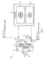
- FIG. 1 is a schematic representation of a system for determining a position of a magnetic member, according to one embodiment of the invention.
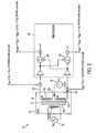
- FIG. 2 is a schematic representation of a system for determining a position of a magnetic member, in accordance with one embodiment of the invention.
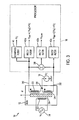
- FIG. 3 is a schematic representation of a system for determining a position of a magnetic member, according to one embodiment of the invention.
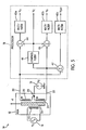
- FIG. 4 is a schematic representation of a system for determining a position of a magnetic member, in accordance with one embodiment of the invention.
- FIG. 5 is a schematic representation of a system for determining a position of a magnetic member, according to one embodiment of the invention.
- FIG. 6 is a schematic representation of a system for determining a position of a magnetic member, in accordance with one embodiment of the invention.
- FIG. 7 is a schematic representation of a system for determining a position of a magnetic member, according to one embodiment of the invention.
- FIG. 8 is a schematic representation of a system for determining a position of a magnetic member, in accordance with one embodiment of the invention.
- FIG. 9 is a schematic representation of a system for determining a position of a magnetic member, according to one embodiment of the invention.
- FIG. 1 is an exemplary illustration of a system 10 for detecting position that is capable of self-monitoring for connectivity faults, according to one embodiment of the invention.
- System 10 includes a linear variable differential transformer 12, an excitation potential source 14, a bias potential source 16, and a processor 18.
- transformer 12 includes a primary coil 20, a first secondary coil 22, a second secondary coil 24, and a magnetic member 26.
- Primary coil 20 is electrically coupled with excitation potential source 14 such that an excitation potential ( V E ) is applied to primary coil 20 by excitation potential source 14.
- First and second secondary coils 22 and 24 are located proximate to primary coil 20 such that the application of the excitation potential to primary coil 20 induces a first induced potential ( V A ) in first secondary coil 22 and a second induced potential ( V B ) in second secondary coil 24.
- Magnetic member 26 is slideably disposed between primary coil 20 and secondary coils 22 and 24.
- a junction 28 electrically couples first secondary coil 22 and secondary coil 24, thereby coupling secondary coils 22 and 24 to each other.
- junction 28 is also electrically coupled to bias potential source 16, which applies a bias potential ( V C ) to junction 28.
- junction 28 may be coupled to alternative potential sources/sinks, as will be described below.
- a first lead 30 electrically couples first secondary coil 22 to processor 18, and a second lead 32 electrically couples second secondary coil 24 to processor 18.
- first lead 30 transmits an output signal from first secondary coil 22 to processor 18 that has a first output potential ( V AA ).
- Second lead 32 transmits an output signal from second secondary coil 24 to processor 18 that has a second output potential ( V BB ).
- first and second output potentials V AA and V BB may be represented as: and
- the potentials V A and V B induced in each of first secondary coil 22 and second secondary coil 24, respectively, vary based on the position of magnetic member 26. More particularly, in an embodiment like the one shown in FIG. 1 , as magnetic member 26 is linearly displaced by a distance d , the potentials V A and V B may be described mathematically as follows: and where N M represents the voltage ratio between V E and V A (or V B ), ⁇ represents the frequency of the excitation potential, K represents a proportionality constant, and t represents time.
- processor 18 includes a position determining module 34 and a fault detection module 36.
- processor 18 may include a plurality of processors connected via an operative link.
- the plurality of processors may be located centrally in a single location.
- one or more of the plurality of processors may be located remotely from each other.
- the operative link(s) between the plurality of processors may include a communications link, such as a wired, or wireless communications link, and may include a connection established over a network, or via a direct connection.
- modules 34 and 36 are provided for illustrative purposes, and that each module may include one or more components that perform the functionalities assigned to modules 34 and 36, as well as other functions. Modules 34 and 36 may include components implemented as hardware, software, firmware, a combination of hardware, software, and/or firmware, as well as in other mediums.
- position determining module 34 determines the position of magnetic member 26 with respect to secondary coils 22 and 24.
- Position determining module 34 may leverage a predetermined relationship between the first and second output potentials V AA and V BB (and/or the potentials V A and V B that are induced in secondary coils 22 and 24). For example, the following relationship may be used to determine the position of magnetic member 26: where, again, K is a proportionality constant, and d is a distance that magnetic member 26 has been displaced. This relationship can be expressed in terms of the output potentials V AA and V BB (using eqns. 1 and 2) as follows:
- fault detection module 36 is capable of detecting faults (e . g ., shorts, opens, etc .) within transformer 12. More particularly, fault detection module 36 is capable of detecting connectivity faults at the electrical connections between excitation potential source 14 and primary coil 20, between first lead 30 and first secondary coil 22, between first secondary coil 22 and junction 28, between junction 28 and bias potential source 16, between junction 28 and second secondary coil 24, and between second lead 32 and secondary coil 24. To detect some of the possible faults within transformer 12, fault detection module 36 monitors the output signals on first lead 30 and second lead 32 to determine if the bias potential is present in each of the output signals. If the bias potential is present in each of the signals, then no faults are present between first lead 30 and second lead 32.
- fault detection module 36 monitors the output signals on first lead 30 and second lead 32 to determine if the bias potential is present in each of the output signals. If the bias potential is present in each of the signals, then no faults are present between first lead 30 and second lead 32.
- bias potential is present in the output signal on first lead 30, but is not present in the output signal on second lead 32, then there is a fault between bias potential source 16 and second lead 32. If the bias potential is present in the output signal on second lead 32, but is not present in the output signal on first lead 30, then there is a fault between bias potential source 16 and first lead 30. If the bias potential is not present in either of the output signals, then there is a fault somewhere between first lead 30 and second lead 32. If the bias potential is present in both output signals, but neither output signal includes an induced potential, then there is a fault in the electronic coupling between excitation potential source 14 and primary coil 20.
- FIG. 2 is an illustration of system 10 configured according to one embodiment of the invention.
- processor 18 includes an adder circuit 38 and a differencing circuit 40.
- Each of adder circuit 38 and differencing circuit 40 are electrically coupled to both of first lead 30 and second lead 32.
- Adder circuit 38 adds the output signals on first lead 30 and second lead 32 such the potential of the signal output from adder circuit 38 is a sum potential ( V SUM ) that includes the sum of the outlet potentials V AA and V BB .
- V SUM may be represented as follows: Differencing circuit 40 subtract the output potential V B on second lead 32 from the output potential V A on first lead 30 to generate a signal at a difference potential ( V DIFF ), which may be represented as: Combining the output signals via adder circuit 38 and differencing circuit 40, enables equation 6, which is used by processor 18 to determine the position of magnetic member 26, to be simplified, using the sum potential V SUM and the difference potential V DIFF , as:
- excitation potential source 14 is an AC potential source
- bias potential source 16 is a DC potential source.
- This may enhance various aspects of the system 10, including separating the induced potentials V A and V B from the bias potential V C for the purpose of fault detection.
- the output potentials, or various combinations thereof e . g ., V SUM and V DIFF
- some or all of the various potentials may be demodulated before they are used to determine the position of magnetic member 26 and/or to detect faults.
- Various demodulation techniques may be executed by processor 18 using software tools, hardware ( e . g ., circuits), or some combination thereof.
- potentials such as the output potential
- V E potentials
- V DIFF potential proportional to, and in phase with, the excitation potential V E .
- the resulting product yields two potentials, one that is periodic at twice the frequency of the excitation potential V E , and one that is not periodic.
- the periodic component may then be discarded, and the non-periodic potential may be used for further processing.
- this demodulation technique is executed below with respect to the induced potential V DIFF . which simplifies to: where the potential ( V D ) that the induced potential V DIFF is multiplied by is expressed mathematically as: where D is an amplitude of the potential V D , and ⁇ is the frequency of the excitation potential V E .
- signals may be demodulated via demodulation circuits within processor 18.
- FIG. 3 illustrates an embodiment of system 10 in which rectifier circuits 42 (illustrated as rectifier circuits 42a-42c) may be used to demodulate potentials to generate demodulated potentials. The demodulated potentials are then be processed further within processor 18 to determine the position of magnetic member 26 and/or detect connectivity faults within transformer 12.
- processor 18 includes adder circuit 38, but not differencing circuit 40.
- the difference potential V DIFF is determined by subtracting potential V BB from potential V AA .
- FIG. 4 illustrates an embodiment of system 10 in which this inability to readily detect a short between secondary coils 22 and 24 is avoided.
- processor 18 includes differencing circuit 40, and secondary coils 22 and 24 are wound in opposite directions so that the induced potentials V A and V B be 180° out of phase. Because of the phase shift between induced potentials V A and V B , the potential yielded by differencing circuit 40 will be the sum potential V SUM , making the potentials used for further processing within processor 18 the same in the embodiments of both FIGS. 3 and 4 . But, in the event of a short between secondary coils 22 and 24, induced potentials V A and V B will destructively interfere, thereby simplifying detection of the short by processor 18.
- the bias potential V C is extracted from one of the output potentials V AA and V BB via a low pass filter 41.
- Low pass filter 41 extracts the DC component of the output potential, the DC component being, essentially, the bias potential V C .
- the extracted bias potential V C is then used within processor 18 in further processing, such as, determining the position of magnetic member 26 and detecting connectivity faults within transformer 12.
- FIG. 5 illustrates another configuration of system 10, according to one embodiment of the invention.
- the bias potential is extracted from one of the output signals and is then subtracted from each of the output potentials V AA and V BB by a pair of differencing circuits 44 and 46, to yield the induced potentials V A and V B , prior to demodulation by rectifier circuits 42.
- a differencing circuit 47 subtracts output potential V AA from V BB to yield a detection potential V DIFF that is independent from the position of the magnetic member 26.
- system 10 may be configured such that the output potentials V AA and V BB are in phase with each other, and the following relationship is leveraged to provide V DIFF with a constant amplitude in the absence of connectivity faults.
- both Vc and V DIFF are monitored within processor 18 for changes that signify a connectivity fault in transformer 12.
- system 10 is shown according to one embodiment of the invention, in which system 10 is wired the substantially the same as in the configuration shown in FIG. 5 .
- processor 18 includes a commercial off-the-shelf LVDT/RVDT signal conditioning chip 49, such as the Analog Devices AD598 (patent pending) that performs as position determination module 34 to determine the position of magnetic member 26.
- the output signals are AC coupled into the signal conditioning chip to remove the bias potential V C .
- the signal conditioning chip can then compute position as if no bias were present in system 10. Two additional potentials are produced in this configuration, the bias potential V C , which is extracted from one of the output potentials as was done in the configuration of FIG.
- V DET which corresponds to the detection potential V DET of the configuration of FIG. 5 discussed above.
- both V BIAS and V DET can be expected to remain constant independent from the position of magnetic member 26, and are monitored to ensure proper operation of transformer 12.
- differencing circuit 40 shown in FIG. 6 may be replaced with an adder circuit that would produce V DET , provided the phasing of transformer 12 was arranged properly.
- FIGS. 1-6 have included 5-wire transformers. It may be appreciated that the present invention also contemplates applying a bias potential V C to other position detecting transformers.
- FIG. 7 illustrates an embodiment of system 10 including a 4-wire linear variable differential transformer 48 in place of the 5-wire transformer 12. Within transformer 48, components similar to those included in transformer 12 are given the same reference numbers. The most notable difference between transformer 48 and transformer 12 is that in transformer 48 junction 28 is electrically coupled to each of first secondary coil 22 and second secondary coil 24, but junction 28 is not coupled to a potential sink ( e . g ., ground) or a potential source ( e . g ., bias potential source 16).
- a potential sink e . g ., ground
- a potential source e . g ., bias potential source 16
- bias potential source 16 is connected to transformer 48 at first lead 30 to apply the bias potential V C to transformer 48.
- the output at second lead 32 therefore, includes the bias potential V C , as well as the induced potentials V A and V B .
- the bias potential V C is extracted from the output signal on second lead 32, and this potential is then monitored by processor 18 to detect connectivity faults within transformer 48.
- position determining module 34 includes a signal conditioning chip 50 applying a conventional demodulation scheme, which may be similar to chip 49 described above.
- the output signal present on second lead 32 is AC coupled into chip 50 to remove the bias potential V C from the output signal.
- FIG. 8 illustrates another configuration of system 10 including transformer 48, according to one embodiment of the invention.
- bias potential source 16 is again applied to transformer 48 on first lead 30, but unlike the configuration shown in FIG. 7 , output signals on both first lead 30 and second lead 32 are AC coupled into chip 50 for enhanced noise immunity.
- FIG. 9 illustrates a configuration of system 10 according to another embodiment of the invention.
- the configuration of system 10 is similar to the configuration of FIG. 8 , but includes a passive network 52 that couples the bias potential V C onto first lead 30 from bias potential source 16.
- Passive network 52 is an electronic network that has a low impedance at DC and a high impedance at the excitation frequency of excitation potential source 14.
- the embodiments of the invention discussed above are described including linear variable differential transformers, it should be appreciated that this is for illustrative purposes only, and that the invention contemplates implementing a bias potential to detect connectivity faults in other types of transformers capable of determining a position of a member within the transformer.
- the invention contemplates rotational variable differential transformers, synchros, and resolvers.
- the descriptions of the embodiments above have disclosed the bias potential V C as a DC potential, however, in another embodiment of the invention the bias potential V C is an AC potential.
Landscapes
- Physics & Mathematics (AREA)
- General Physics & Mathematics (AREA)
- Transmission And Conversion Of Sensor Element Output (AREA)
- Measurement Of Length, Angles, Or The Like Using Electric Or Magnetic Means (AREA)
- Testing Of Short-Circuits, Discontinuities, Leakage, Or Incorrect Line Connections (AREA)
- Locating Faults (AREA)
- Tests Of Electronic Circuits (AREA)
- Investigating Or Analyzing Materials By The Use Of Magnetic Means (AREA)
- Measurement Of Velocity Or Position Using Acoustic Or Ultrasonic Waves (AREA)
Claims (13)
- Positionserfassungssystem, das in der Lage ist, Konnektivitätsfehler selbst zu überwachen, wobei das System umfasst:einen Transformator, in dem ein Magnetelement beweglich angeordnet ist; eine Anregungspotenzial-Quelle, die mit dem Transformator gekoppelt ist, um ein Anregungspotenzial an den Transformator anzulegen, wobei das Anlegen eines Anregungspotenzials an den Transformator zumindest ein induziertes Potenzial induziert, das von der Stellung des Magnetelements in dem Transformator abhängig ist,eine Vorspannungspotenzial-Quelle, die mit dem Transformator gekoppelt ist, um ein Vorspannungspotenzial an den Transformator anzulegen;einen Prozessor, der mit dem Transformator gekoppelt ist, um zumindest ein Ausgabesignal zu empfangen, wobei das zumindest eine Ausgabesignal das zumindest eine induzierte Potenzial einschließt,wobei der Prozessor die Stellung des Magnetelements aufgrund des zumindest einen Induktionspotenzials bestimmt und
der Prozessor Konnektivitätsfehler in dem Transformator aufgrund des Vorhandenseins oder Fehlens des Vorspannungspotenzials in dem Ausgabesignal detektiert. - System nach Anspruch 1, wobei der Transformator umfasst:eine Primärspule, die derart mit der Anregungspotenzial-Quelle gekoppelt ist, dass das Anregungspotenzial an die Primärspule angelegt wird;eine erste Sekundärspule, die benachbart der Primärspule derart angeordnet ist, dass das Anlegen des Anregungspotenzials an die Primärspule ein erstes Induktionspotenzial in der ersten Sekundärspule induziert;eine zweite Sekundärspule, die benachbart der Primärspule derart angeordnet ist, dass das Anlegen des Anregungspotenzials an die Primärspule ein zweites Induktionspotenzial in der zweiten Sekundärspule induziert; undeinen Verbindungsübergang, der jeweils mit der ersten Sekundärspule und der zweiten Sekundärspule gekoppelt ist;wobei die Vorspannungspotenzial-Quelle mit dem Verbindungsübergang gekoppelt ist und das Vorspannungspotenzial an den Verbindungsübergang anlegt.
- System nach Anspruch 1, wobei der Transformator umfasst:eine Primärspule, die derart mit der Anregungspotenzial-Quelle gekoppelt ist, dass das Anregungspotenzial an die Primärspule angelegt wird;eine erste Sekundärspule, die benachbart der Primärspule derart angeordnet ist, dass das Anlegen des Anregungspotenzials an die Primärspule ein erstes Induktionspotenzial in der ersten Sekundärspule induziert;eine zweite Sekundärspule, die benachbart der Primärspule derart angeordnet ist, dass das Anlegen des Anregungspotenzials an die Primärspule ein zweites Induktionspotenzial in der zweiten Sekundärspule induziert;eine erste Anschlussleitung, die mit der ersten Sekundärspule gekoppelt ist; undeine zweite Anschlussleitung, die mit der zweiten Sekundärspule gekoppelt ist,wobei die Vorspannungspotenzial-Quelle derart mit der ersten Anschlussleitung bzw. mit der zweiten Anschlussleitung gekoppelt ist, dass das Vorspannungspotenzial an die erste Anschlussleitung bzw. an die zweite Anschlussleitung angelegt wird.
- System nach Anspruch 1, wobei eine Drehrichtung des Magnetelements durch den Prozessor bestimmt wird.
- System nach Anspruch 1, wobei eine Linearverschiebung des Magnetelements durch den Prozessor bestimmt wird.
- System nach Anspruch 1, wobei es sich bei dem Anregungspotenzial um ein Wechselstrompotenzial und bei dem Vorspannungspotenzial um ein Gleichspannungspotenzial handelt.
- System nach Anspruch 1, wobei es sich bei dem Anregungspotenzial und dem Vorspannungspotenzial um Wechselstrompotenziale handelt.
- System nach Anspruch 1, wobei der Transformator einen Drehwinkelmelder umfasst.
- System nach Anspruch 1, wobei der Transformator einen Winkellagegeber umfasst.
- System nach Anspruch 1, wobei der Transformator einen linear variablen Differenzialtransformator umfasst.
- System nach Anspruch 1, wobei der Transformator einen drehvariablen Differenzialtransformator umfasst.
- System nach Anspruch 1, wobei der Transformator einen 5-Draht-Transformator umfasst.
- System nach Anspruch 1, wobei der Transformator einen 4-Draht-Transformator umfasst.
Applications Claiming Priority (2)
| Application Number | Priority Date | Filing Date | Title |
|---|---|---|---|
| US11/314,163 US7288933B2 (en) | 2005-12-22 | 2005-12-22 | Position detecting system that self-monitors for connectivity faults |
| PCT/US2006/062477 WO2007089372A2 (en) | 2005-12-22 | 2006-12-21 | A position detecting system that self-monitors for connectivity faults |
Publications (2)
| Publication Number | Publication Date |
|---|---|
| EP1963785A2 EP1963785A2 (de) | 2008-09-03 |
| EP1963785B1 true EP1963785B1 (de) | 2009-06-17 |
Family
ID=38193397
Family Applications (1)
| Application Number | Title | Priority Date | Filing Date |
|---|---|---|---|
| EP06850423A Active EP1963785B1 (de) | 2005-12-22 | 2006-12-21 | Positionserfassungssystem mit selbstüberwachung für konnektivitätsfehler |
Country Status (12)
| Country | Link |
|---|---|
| US (1) | US7288933B2 (de) |
| EP (1) | EP1963785B1 (de) |
| JP (1) | JP2009521691A (de) |
| KR (1) | KR20080083645A (de) |
| CN (1) | CN101346607B (de) |
| AT (1) | ATE434169T1 (de) |
| AU (1) | AU2006337090A1 (de) |
| BR (1) | BRPI0620284A2 (de) |
| CA (1) | CA2633511C (de) |
| DE (1) | DE602006007379D1 (de) |
| RU (1) | RU2008130092A (de) |
| WO (1) | WO2007089372A2 (de) |
Families Citing this family (17)
| Publication number | Priority date | Publication date | Assignee | Title |
|---|---|---|---|---|
| US8154305B2 (en) | 2010-07-16 | 2012-04-10 | General Electric Company | Systems, methods, and apparatus for connection fault self-monitoring with DC bias current |
| US9383228B2 (en) * | 2012-12-03 | 2016-07-05 | Hamilton Sundstrand Corporation | Control voltage signal synthesis system and method |
| JP2014188122A (ja) * | 2013-03-27 | 2014-10-06 | Akita Prefectural Hospital Organization | 磁性体検出センサ、磁性体検出方法および磁性体検出装置 |
| US9448275B2 (en) * | 2013-06-25 | 2016-09-20 | The Boeing Company | Fault detection of four wire variable differential transformer sensors |
| DE102013219657A1 (de) * | 2013-09-27 | 2015-04-02 | Continental Teves Ag & Co. Ohg | Verfahren zum Testen eines Transformators |
| EP3100065B1 (de) * | 2014-01-31 | 2018-12-26 | University Of South Australia | Sensor zur detektion von magnetischen partikeln |
| CN106164623B (zh) | 2014-03-31 | 2019-04-16 | 庞巴迪公司 | 用于检测传感器与受控元件的机械断开的系统 |
| CN105527530B (zh) * | 2014-09-28 | 2018-07-06 | 中国航空工业集团公司西安飞机设计研究所 | 一种位移传感器断线的检测电路、方法及其信号重构方法 |
| CN105527906B (zh) * | 2014-09-28 | 2018-03-02 | 中国航空工业集团公司西安飞机设计研究所 | 一种位移传感器接收通道的监控电路 |
| DE102015211224A1 (de) * | 2015-06-18 | 2016-12-22 | Robert Bosch Gmbh | Verfahren und Schaltung zum Erkennen einer offenen Resolver-Erregerleitung |
| DE102015211216A1 (de) * | 2015-06-18 | 2016-12-22 | Robert Bosch Gmbh | Verfahren und Schaltung zum Erkennen eines Kurzschlusses der Sinus- oder Kosinus-Empfängerspule eines Resolvers |
| US9817061B2 (en) * | 2015-07-16 | 2017-11-14 | The Boeing Company | Linear variable differential transformer (LVDT) secondary wiring intermittent failure monitor |
| US10345357B2 (en) | 2016-02-29 | 2019-07-09 | The Boeing Company | Fault detection in variable differential transformer sensors based on zero-crossings of signals |
| JP6881582B2 (ja) * | 2017-07-21 | 2021-06-02 | 株式会社島津製作所 | 磁性体の検査装置 |
| US10756531B2 (en) * | 2018-03-29 | 2020-08-25 | Hamilton Sunstrand Corporation | Voltage differential transducer (VDT) fault detection |
| CN109163648A (zh) * | 2018-08-24 | 2019-01-08 | 中国飞机强度研究所 | 位移测量故障检测方法及装置 |
| US20250149238A1 (en) * | 2023-11-02 | 2025-05-08 | Woodward, Inc. | Systems and methods for variable differential transformers secondaries with single rail bias |
Family Cites Families (9)
| Publication number | Priority date | Publication date | Assignee | Title |
|---|---|---|---|---|
| US3859567A (en) * | 1973-04-23 | 1975-01-07 | Amf Inc | Ground fault interrupter circuit with excited secondary winding on differential transformer |
| US4162491A (en) * | 1978-01-11 | 1979-07-24 | Avco Corporation | Inductive position sensor with minimum output signal level capacitively coupled to indicate failure of device |
| SE452533B (sv) * | 1986-04-08 | 1987-11-30 | Asea Ab | Forfarande for riktningsdetektering av fel pa en kraftledning samt anordning for genomforande av det nemnda forfarandet |
| US5109675A (en) * | 1990-10-10 | 1992-05-05 | Westinghouse Electric Corp. | Valve position sensing circuit |
| CH684216A5 (fr) * | 1991-02-15 | 1994-07-29 | Lem Liaisons Electron Mec | Dispositif de mesure de courants. |
| TW406465B (en) * | 1997-04-07 | 2000-09-21 | Cts Corp | Control circuits for generating control signals proportional to the position of an input device |
| US6636035B2 (en) * | 2000-03-13 | 2003-10-21 | Mitutoyo Corporation | Position measuring device and error detecting method for the same, and electromagnetic induction position detecting device |
| US6885949B2 (en) * | 2002-07-24 | 2005-04-26 | Smar Research Corporation | System and method for measuring system parameters and process variables using multiple sensors which are isolated by an intrinsically safe barrier |
| AU2003298124A1 (en) * | 2002-11-20 | 2004-06-15 | Walter Mehnert | Position detector |
-
2005
- 2005-12-22 US US11/314,163 patent/US7288933B2/en not_active Expired - Lifetime
-
2006
- 2006-12-21 JP JP2008547769A patent/JP2009521691A/ja active Pending
- 2006-12-21 CA CA2633511A patent/CA2633511C/en active Active
- 2006-12-21 WO PCT/US2006/062477 patent/WO2007089372A2/en not_active Ceased
- 2006-12-21 BR BRPI0620284-5A patent/BRPI0620284A2/pt not_active Application Discontinuation
- 2006-12-21 AU AU2006337090A patent/AU2006337090A1/en not_active Abandoned
- 2006-12-21 EP EP06850423A patent/EP1963785B1/de active Active
- 2006-12-21 DE DE602006007379T patent/DE602006007379D1/de active Active
- 2006-12-21 KR KR1020087015110A patent/KR20080083645A/ko not_active Withdrawn
- 2006-12-21 AT AT06850423T patent/ATE434169T1/de not_active IP Right Cessation
- 2006-12-21 CN CN2006800485082A patent/CN101346607B/zh not_active Expired - Fee Related
- 2006-12-21 RU RU2008130092/28A patent/RU2008130092A/ru unknown
Also Published As
| Publication number | Publication date |
|---|---|
| WO2007089372A3 (en) | 2007-11-29 |
| ATE434169T1 (de) | 2009-07-15 |
| AU2006337090A1 (en) | 2007-08-09 |
| RU2008130092A (ru) | 2010-01-27 |
| CA2633511C (en) | 2014-04-22 |
| KR20080083645A (ko) | 2008-09-18 |
| US20070146942A1 (en) | 2007-06-28 |
| CN101346607B (zh) | 2010-10-20 |
| US7288933B2 (en) | 2007-10-30 |
| EP1963785A2 (de) | 2008-09-03 |
| CA2633511A1 (en) | 2007-08-09 |
| CN101346607A (zh) | 2009-01-14 |
| BRPI0620284A2 (pt) | 2011-11-08 |
| WO2007089372A2 (en) | 2007-08-09 |
| JP2009521691A (ja) | 2009-06-04 |
| DE602006007379D1 (de) | 2009-07-30 |
Similar Documents
| Publication | Publication Date | Title |
|---|---|---|
| US7288933B2 (en) | Position detecting system that self-monitors for connectivity faults | |
| EP0087271B1 (de) | Elektromagnetisches System und Gerät zur geophysikalischen Überwachung | |
| JP2018004630A (ja) | 電子式アブソリュート型エンコーダ | |
| EP3161962B1 (de) | Kompensation der kopplung eines zielobjekts an versorgungsleitungen in einem kapazitiven sensorsystem | |
| US20070085698A1 (en) | Enhanced sonde recognition | |
| EP2756316B1 (de) | Schema zur erzielung einer beständigkeit gegen elektromagnetische interferenz von trägheitssensoren | |
| US20130154674A1 (en) | Method of high voltage detection and accurate phase angle measurement in cordless phasing meters | |
| JP2013511080A (ja) | 複数のセンサー素子に対するセンサーエレクトロニクスおよびセンサー素子における物体の位置を決定する方法 | |
| JP2013252040A (ja) | 非接触給電システムの漏電診断装置 | |
| JP5684125B2 (ja) | 手足の位置又は位置の変化の指標となる信号を生成するためのセンサ・デバイス | |
| US9506969B2 (en) | Noise sensor | |
| US6853180B2 (en) | Measured value acquisition and processing unit for small measuring signals | |
| US10054709B2 (en) | Object locater and method for locating a metallic and/or magnetizable object | |
| EP2350569B1 (de) | Induktiver winkelsensor mit verbesserter gleichtaktrauschunterdrückung und signalverarbeitungsverfahren dafür | |
| JP3802028B2 (ja) | 光電流センサを用いる保護継電装置 | |
| US20130173198A1 (en) | Circuit arrangement and method for monitoring a dsp in the context of a safety-critical application | |
| US7567875B2 (en) | Enhanced sonde recognition | |
| KR20090100489A (ko) | 내잡음성을 향상시킨 인덕턴스방식 앵글센서 및 그신호처리방법 | |
| JP4633890B2 (ja) | 把握式の零相変流器を用いた実効漏電計 | |
| Lawrence | Hardware and software architecture for non-contact, non-intrusive load monitoring | |
| JPH0833454B2 (ja) | 埋設物の探知装置 | |
| EP4707745A1 (de) | Induktiver positionssensor | |
| RU2153650C2 (ru) | Способ выделения сигналов дифференциального датчика | |
| RU2066043C1 (ru) | Тензопреобразователь | |
| KR102451512B1 (ko) | 신호를 등록하고 처리하기 위한 측정 회로, 및 상기 측정 회로를 사용하기 위한 측정 장치 |
Legal Events
| Date | Code | Title | Description |
|---|---|---|---|
| PUAI | Public reference made under article 153(3) epc to a published international application that has entered the european phase |
Free format text: ORIGINAL CODE: 0009012 |
|
| 17P | Request for examination filed |
Effective date: 20080606 |
|
| AK | Designated contracting states |
Kind code of ref document: A2 Designated state(s): AT BE BG CH CY CZ DE DK EE ES FI FR GB GR HU IE IS IT LI LT LU LV MC NL PL PT RO SE SI SK TR |
|
| GRAP | Despatch of communication of intention to grant a patent |
Free format text: ORIGINAL CODE: EPIDOSNIGR1 |
|
| GRAS | Grant fee paid |
Free format text: ORIGINAL CODE: EPIDOSNIGR3 |
|
| GRAA | (expected) grant |
Free format text: ORIGINAL CODE: 0009210 |
|
| AK | Designated contracting states |
Kind code of ref document: B1 Designated state(s): AT BE BG CH CY CZ DE DK EE ES FI FR GB GR HU IE IS IT LI LT LU LV MC NL PL PT RO SE SI SK TR |
|
| REG | Reference to a national code |
Ref country code: GB Ref legal event code: FG4D |
|
| REG | Reference to a national code |
Ref country code: CH Ref legal event code: EP |
|
| REG | Reference to a national code |
Ref country code: IE Ref legal event code: FG4D |
|
| REF | Corresponds to: |
Ref document number: 602006007379 Country of ref document: DE Date of ref document: 20090730 Kind code of ref document: P |
|
| PG25 | Lapsed in a contracting state [announced via postgrant information from national office to epo] |
Ref country code: LT Free format text: LAPSE BECAUSE OF FAILURE TO SUBMIT A TRANSLATION OF THE DESCRIPTION OR TO PAY THE FEE WITHIN THE PRESCRIBED TIME-LIMIT Effective date: 20090617 Ref country code: FI Free format text: LAPSE BECAUSE OF FAILURE TO SUBMIT A TRANSLATION OF THE DESCRIPTION OR TO PAY THE FEE WITHIN THE PRESCRIBED TIME-LIMIT Effective date: 20090617 Ref country code: AT Free format text: LAPSE BECAUSE OF FAILURE TO SUBMIT A TRANSLATION OF THE DESCRIPTION OR TO PAY THE FEE WITHIN THE PRESCRIBED TIME-LIMIT Effective date: 20090617 |
|
| PG25 | Lapsed in a contracting state [announced via postgrant information from national office to epo] |
Ref country code: SI Free format text: LAPSE BECAUSE OF FAILURE TO SUBMIT A TRANSLATION OF THE DESCRIPTION OR TO PAY THE FEE WITHIN THE PRESCRIBED TIME-LIMIT Effective date: 20090617 Ref country code: LV Free format text: LAPSE BECAUSE OF FAILURE TO SUBMIT A TRANSLATION OF THE DESCRIPTION OR TO PAY THE FEE WITHIN THE PRESCRIBED TIME-LIMIT Effective date: 20090617 Ref country code: SE Free format text: LAPSE BECAUSE OF FAILURE TO SUBMIT A TRANSLATION OF THE DESCRIPTION OR TO PAY THE FEE WITHIN THE PRESCRIBED TIME-LIMIT Effective date: 20090917 Ref country code: PL Free format text: LAPSE BECAUSE OF FAILURE TO SUBMIT A TRANSLATION OF THE DESCRIPTION OR TO PAY THE FEE WITHIN THE PRESCRIBED TIME-LIMIT Effective date: 20090617 |
|
| NLV1 | Nl: lapsed or annulled due to failure to fulfill the requirements of art. 29p and 29m of the patents act | ||
| PG25 | Lapsed in a contracting state [announced via postgrant information from national office to epo] |
Ref country code: CZ Free format text: LAPSE BECAUSE OF FAILURE TO SUBMIT A TRANSLATION OF THE DESCRIPTION OR TO PAY THE FEE WITHIN THE PRESCRIBED TIME-LIMIT Effective date: 20090617 Ref country code: ES Free format text: LAPSE BECAUSE OF FAILURE TO SUBMIT A TRANSLATION OF THE DESCRIPTION OR TO PAY THE FEE WITHIN THE PRESCRIBED TIME-LIMIT Effective date: 20090928 Ref country code: IS Free format text: LAPSE BECAUSE OF FAILURE TO SUBMIT A TRANSLATION OF THE DESCRIPTION OR TO PAY THE FEE WITHIN THE PRESCRIBED TIME-LIMIT Effective date: 20091017 Ref country code: RO Free format text: LAPSE BECAUSE OF FAILURE TO SUBMIT A TRANSLATION OF THE DESCRIPTION OR TO PAY THE FEE WITHIN THE PRESCRIBED TIME-LIMIT Effective date: 20090617 Ref country code: EE Free format text: LAPSE BECAUSE OF FAILURE TO SUBMIT A TRANSLATION OF THE DESCRIPTION OR TO PAY THE FEE WITHIN THE PRESCRIBED TIME-LIMIT Effective date: 20090617 |
|
| PG25 | Lapsed in a contracting state [announced via postgrant information from national office to epo] |
Ref country code: SK Free format text: LAPSE BECAUSE OF FAILURE TO SUBMIT A TRANSLATION OF THE DESCRIPTION OR TO PAY THE FEE WITHIN THE PRESCRIBED TIME-LIMIT Effective date: 20090617 Ref country code: BE Free format text: LAPSE BECAUSE OF FAILURE TO SUBMIT A TRANSLATION OF THE DESCRIPTION OR TO PAY THE FEE WITHIN THE PRESCRIBED TIME-LIMIT Effective date: 20090617 Ref country code: NL Free format text: LAPSE BECAUSE OF FAILURE TO SUBMIT A TRANSLATION OF THE DESCRIPTION OR TO PAY THE FEE WITHIN THE PRESCRIBED TIME-LIMIT Effective date: 20090617 |
|
| PG25 | Lapsed in a contracting state [announced via postgrant information from national office to epo] |
Ref country code: BG Free format text: LAPSE BECAUSE OF FAILURE TO SUBMIT A TRANSLATION OF THE DESCRIPTION OR TO PAY THE FEE WITHIN THE PRESCRIBED TIME-LIMIT Effective date: 20090917 Ref country code: PT Free format text: LAPSE BECAUSE OF FAILURE TO SUBMIT A TRANSLATION OF THE DESCRIPTION OR TO PAY THE FEE WITHIN THE PRESCRIBED TIME-LIMIT Effective date: 20091017 |
|
| PLBE | No opposition filed within time limit |
Free format text: ORIGINAL CODE: 0009261 |
|
| STAA | Information on the status of an ep patent application or granted ep patent |
Free format text: STATUS: NO OPPOSITION FILED WITHIN TIME LIMIT |
|
| PG25 | Lapsed in a contracting state [announced via postgrant information from national office to epo] |
Ref country code: DK Free format text: LAPSE BECAUSE OF FAILURE TO SUBMIT A TRANSLATION OF THE DESCRIPTION OR TO PAY THE FEE WITHIN THE PRESCRIBED TIME-LIMIT Effective date: 20090617 |
|
| 26N | No opposition filed |
Effective date: 20100318 |
|
| PG25 | Lapsed in a contracting state [announced via postgrant information from national office to epo] |
Ref country code: MC Free format text: LAPSE BECAUSE OF NON-PAYMENT OF DUE FEES Effective date: 20100701 |
|
| PG25 | Lapsed in a contracting state [announced via postgrant information from national office to epo] |
Ref country code: GR Free format text: LAPSE BECAUSE OF FAILURE TO SUBMIT A TRANSLATION OF THE DESCRIPTION OR TO PAY THE FEE WITHIN THE PRESCRIBED TIME-LIMIT Effective date: 20090918 Ref country code: IE Free format text: LAPSE BECAUSE OF NON-PAYMENT OF DUE FEES Effective date: 20091221 |
|
| PG25 | Lapsed in a contracting state [announced via postgrant information from national office to epo] |
Ref country code: LU Free format text: LAPSE BECAUSE OF NON-PAYMENT OF DUE FEES Effective date: 20091221 |
|
| PG25 | Lapsed in a contracting state [announced via postgrant information from national office to epo] |
Ref country code: HU Free format text: LAPSE BECAUSE OF FAILURE TO SUBMIT A TRANSLATION OF THE DESCRIPTION OR TO PAY THE FEE WITHIN THE PRESCRIBED TIME-LIMIT Effective date: 20091218 |
|
| REG | Reference to a national code |
Ref country code: CH Ref legal event code: PL |
|
| PG25 | Lapsed in a contracting state [announced via postgrant information from national office to epo] |
Ref country code: TR Free format text: LAPSE BECAUSE OF FAILURE TO SUBMIT A TRANSLATION OF THE DESCRIPTION OR TO PAY THE FEE WITHIN THE PRESCRIBED TIME-LIMIT Effective date: 20090617 |
|
| PG25 | Lapsed in a contracting state [announced via postgrant information from national office to epo] |
Ref country code: CY Free format text: LAPSE BECAUSE OF FAILURE TO SUBMIT A TRANSLATION OF THE DESCRIPTION OR TO PAY THE FEE WITHIN THE PRESCRIBED TIME-LIMIT Effective date: 20090617 |
|
| PG25 | Lapsed in a contracting state [announced via postgrant information from national office to epo] |
Ref country code: LI Free format text: LAPSE BECAUSE OF NON-PAYMENT OF DUE FEES Effective date: 20101231 Ref country code: CH Free format text: LAPSE BECAUSE OF NON-PAYMENT OF DUE FEES Effective date: 20101231 |
|
| REG | Reference to a national code |
Ref country code: FR Ref legal event code: PLFP Year of fee payment: 10 |
|
| REG | Reference to a national code |
Ref country code: FR Ref legal event code: PLFP Year of fee payment: 11 |
|
| PG25 | Lapsed in a contracting state [announced via postgrant information from national office to epo] |
Ref country code: IT Free format text: LAPSE BECAUSE OF NON-PAYMENT OF DUE FEES Effective date: 20151221 |
|
| PG25 | Lapsed in a contracting state [announced via postgrant information from national office to epo] |
Ref country code: IT Free format text: LAPSE BECAUSE OF NON-PAYMENT OF DUE FEES Effective date: 20151221 |
|
| PGRI | Patent reinstated in contracting state [announced from national office to epo] |
Ref country code: IT Effective date: 20170710 |
|
| REG | Reference to a national code |
Ref country code: FR Ref legal event code: PLFP Year of fee payment: 12 |
|
| PGFP | Annual fee paid to national office [announced via postgrant information from national office to epo] |
Ref country code: DE Payment date: 20221228 Year of fee payment: 17 |
|
| PGFP | Annual fee paid to national office [announced via postgrant information from national office to epo] |
Ref country code: FR Payment date: 20231227 Year of fee payment: 18 |
|
| REG | Reference to a national code |
Ref country code: DE Ref legal event code: R119 Ref document number: 602006007379 Country of ref document: DE |
|
| PG25 | Lapsed in a contracting state [announced via postgrant information from national office to epo] |
Ref country code: DE Free format text: LAPSE BECAUSE OF NON-PAYMENT OF DUE FEES Effective date: 20240702 |
|
| PG25 | Lapsed in a contracting state [announced via postgrant information from national office to epo] |
Ref country code: DE Free format text: LAPSE BECAUSE OF NON-PAYMENT OF DUE FEES Effective date: 20240702 |
|
| PG25 | Lapsed in a contracting state [announced via postgrant information from national office to epo] |
Ref country code: FR Free format text: LAPSE BECAUSE OF NON-PAYMENT OF DUE FEES Effective date: 20241231 |
|
| PGFP | Annual fee paid to national office [announced via postgrant information from national office to epo] |
Ref country code: GB Payment date: 20251229 Year of fee payment: 20 |
|
| PGFP | Annual fee paid to national office [announced via postgrant information from national office to epo] |
Ref country code: IT Payment date: 20251219 Year of fee payment: 20 |