EP1970962A1 - Dispositif semi-conducteur et son procédé de fabrication - Google Patents
Dispositif semi-conducteur et son procédé de fabrication Download PDFInfo
- Publication number
- EP1970962A1 EP1970962A1 EP08003214A EP08003214A EP1970962A1 EP 1970962 A1 EP1970962 A1 EP 1970962A1 EP 08003214 A EP08003214 A EP 08003214A EP 08003214 A EP08003214 A EP 08003214A EP 1970962 A1 EP1970962 A1 EP 1970962A1
- Authority
- EP
- European Patent Office
- Prior art keywords
- semiconductor device
- type layer
- support
- conductive material
- semiconductor
- Prior art date
- Legal status (The legal status is an assumption and is not a legal conclusion. Google has not performed a legal analysis and makes no representation as to the accuracy of the status listed.)
- Granted
Links
Images


Classifications
-
- H—ELECTRICITY
- H10—SEMICONDUCTOR DEVICES; ELECTRIC SOLID-STATE DEVICES NOT OTHERWISE PROVIDED FOR
- H10W—GENERIC PACKAGES, INTERCONNECTIONS, CONNECTORS OR OTHER CONSTRUCTIONAL DETAILS OF DEVICES COVERED BY CLASS H10
- H10W72/00—Interconnections or connectors in packages
- H10W72/90—Bond pads, in general
-
- H—ELECTRICITY
- H10—SEMICONDUCTOR DEVICES; ELECTRIC SOLID-STATE DEVICES NOT OTHERWISE PROVIDED FOR
- H10D—INORGANIC ELECTRIC SEMICONDUCTOR DEVICES
- H10D18/00—Thyristors
-
- H—ELECTRICITY
- H10—SEMICONDUCTOR DEVICES; ELECTRIC SOLID-STATE DEVICES NOT OTHERWISE PROVIDED FOR
- H10D—INORGANIC ELECTRIC SEMICONDUCTOR DEVICES
- H10D64/00—Electrodes of devices having potential barriers
- H10D64/20—Electrodes characterised by their shapes, relative sizes or dispositions
- H10D64/23—Electrodes carrying the current to be rectified, amplified, oscillated or switched, e.g. sources, drains, anodes or cathodes
- H10D64/233—Cathode or anode electrodes for thyristors
-
- H—ELECTRICITY
- H10—SEMICONDUCTOR DEVICES; ELECTRIC SOLID-STATE DEVICES NOT OTHERWISE PROVIDED FOR
- H10D—INORGANIC ELECTRIC SEMICONDUCTOR DEVICES
- H10D8/00—Diodes
- H10D8/80—PNPN diodes, e.g. Shockley diodes or break-over diodes
-
- H—ELECTRICITY
- H10—SEMICONDUCTOR DEVICES; ELECTRIC SOLID-STATE DEVICES NOT OTHERWISE PROVIDED FOR
- H10W—GENERIC PACKAGES, INTERCONNECTIONS, CONNECTORS OR OTHER CONSTRUCTIONAL DETAILS OF DEVICES COVERED BY CLASS H10
- H10W70/00—Package substrates; Interposers; Redistribution layers [RDL]
- H10W70/20—Conductive package substrates serving as an interconnection, e.g. metal plates
-
- H—ELECTRICITY
- H10—SEMICONDUCTOR DEVICES; ELECTRIC SOLID-STATE DEVICES NOT OTHERWISE PROVIDED FOR
- H10W—GENERIC PACKAGES, INTERCONNECTIONS, CONNECTORS OR OTHER CONSTRUCTIONAL DETAILS OF DEVICES COVERED BY CLASS H10
- H10W70/00—Package substrates; Interposers; Redistribution layers [RDL]
- H10W70/40—Leadframes
- H10W70/481—Leadframes for devices being provided for in groups H10D8/00 - H10D48/00
-
- H—ELECTRICITY
- H10—SEMICONDUCTOR DEVICES; ELECTRIC SOLID-STATE DEVICES NOT OTHERWISE PROVIDED FOR
- H10W—GENERIC PACKAGES, INTERCONNECTIONS, CONNECTORS OR OTHER CONSTRUCTIONAL DETAILS OF DEVICES COVERED BY CLASS H10
- H10W70/00—Package substrates; Interposers; Redistribution layers [RDL]
- H10W70/60—Insulating or insulated package substrates; Interposers; Redistribution layers
- H10W70/62—Insulating or insulated package substrates; Interposers; Redistribution layers characterised by their interconnections
- H10W70/65—Shapes or dispositions of interconnections
- H10W70/658—Shapes or dispositions of interconnections for devices provided for in groups H10D8/00 - H10D48/00
-
- H—ELECTRICITY
- H10—SEMICONDUCTOR DEVICES; ELECTRIC SOLID-STATE DEVICES NOT OTHERWISE PROVIDED FOR
- H10W—GENERIC PACKAGES, INTERCONNECTIONS, CONNECTORS OR OTHER CONSTRUCTIONAL DETAILS OF DEVICES COVERED BY CLASS H10
- H10W72/00—Interconnections or connectors in packages
-
- H—ELECTRICITY
- H10—SEMICONDUCTOR DEVICES; ELECTRIC SOLID-STATE DEVICES NOT OTHERWISE PROVIDED FOR
- H10W—GENERIC PACKAGES, INTERCONNECTIONS, CONNECTORS OR OTHER CONSTRUCTIONAL DETAILS OF DEVICES COVERED BY CLASS H10
- H10W72/00—Interconnections or connectors in packages
- H10W72/20—Bump connectors, e.g. solder bumps or copper pillars; Dummy bumps; Thermal bumps
-
- H—ELECTRICITY
- H10—SEMICONDUCTOR DEVICES; ELECTRIC SOLID-STATE DEVICES NOT OTHERWISE PROVIDED FOR
- H10W—GENERIC PACKAGES, INTERCONNECTIONS, CONNECTORS OR OTHER CONSTRUCTIONAL DETAILS OF DEVICES COVERED BY CLASS H10
- H10W72/00—Interconnections or connectors in packages
- H10W72/30—Die-attach connectors
-
- H—ELECTRICITY
- H10—SEMICONDUCTOR DEVICES; ELECTRIC SOLID-STATE DEVICES NOT OTHERWISE PROVIDED FOR
- H10W—GENERIC PACKAGES, INTERCONNECTIONS, CONNECTORS OR OTHER CONSTRUCTIONAL DETAILS OF DEVICES COVERED BY CLASS H10
- H10W72/00—Interconnections or connectors in packages
- H10W72/01—Manufacture or treatment
- H10W72/013—Manufacture or treatment of die-attach connectors
- H10W72/01308—Manufacture or treatment of die-attach connectors using permanent auxiliary members, e.g. using alignment marks
-
- H—ELECTRICITY
- H10—SEMICONDUCTOR DEVICES; ELECTRIC SOLID-STATE DEVICES NOT OTHERWISE PROVIDED FOR
- H10W—GENERIC PACKAGES, INTERCONNECTIONS, CONNECTORS OR OTHER CONSTRUCTIONAL DETAILS OF DEVICES COVERED BY CLASS H10
- H10W72/00—Interconnections or connectors in packages
- H10W72/071—Connecting or disconnecting
- H10W72/073—Connecting or disconnecting of die-attach connectors
- H10W72/07321—Aligning
- H10W72/07327—Aligning involving guiding structures, e.g. spacers or supporting members
-
- H—ELECTRICITY
- H10—SEMICONDUCTOR DEVICES; ELECTRIC SOLID-STATE DEVICES NOT OTHERWISE PROVIDED FOR
- H10W—GENERIC PACKAGES, INTERCONNECTIONS, CONNECTORS OR OTHER CONSTRUCTIONAL DETAILS OF DEVICES COVERED BY CLASS H10
- H10W72/00—Interconnections or connectors in packages
- H10W72/071—Connecting or disconnecting
- H10W72/073—Connecting or disconnecting of die-attach connectors
- H10W72/07331—Connecting techniques
- H10W72/07336—Soldering or alloying
-
- H—ELECTRICITY
- H10—SEMICONDUCTOR DEVICES; ELECTRIC SOLID-STATE DEVICES NOT OTHERWISE PROVIDED FOR
- H10W—GENERIC PACKAGES, INTERCONNECTIONS, CONNECTORS OR OTHER CONSTRUCTIONAL DETAILS OF DEVICES COVERED BY CLASS H10
- H10W72/00—Interconnections or connectors in packages
- H10W72/071—Connecting or disconnecting
- H10W72/073—Connecting or disconnecting of die-attach connectors
- H10W72/07351—Connecting or disconnecting of die-attach connectors characterised by changes in properties of the die-attach connectors during connecting
- H10W72/07352—Connecting or disconnecting of die-attach connectors characterised by changes in properties of the die-attach connectors during connecting changes in structures or sizes
-
- H—ELECTRICITY
- H10—SEMICONDUCTOR DEVICES; ELECTRIC SOLID-STATE DEVICES NOT OTHERWISE PROVIDED FOR
- H10W—GENERIC PACKAGES, INTERCONNECTIONS, CONNECTORS OR OTHER CONSTRUCTIONAL DETAILS OF DEVICES COVERED BY CLASS H10
- H10W72/00—Interconnections or connectors in packages
- H10W72/071—Connecting or disconnecting
- H10W72/076—Connecting or disconnecting of strap connectors
- H10W72/07631—Techniques
- H10W72/07636—Soldering or alloying
-
- H—ELECTRICITY
- H10—SEMICONDUCTOR DEVICES; ELECTRIC SOLID-STATE DEVICES NOT OTHERWISE PROVIDED FOR
- H10W—GENERIC PACKAGES, INTERCONNECTIONS, CONNECTORS OR OTHER CONSTRUCTIONAL DETAILS OF DEVICES COVERED BY CLASS H10
- H10W72/00—Interconnections or connectors in packages
- H10W72/30—Die-attach connectors
- H10W72/321—Structures or relative sizes of die-attach connectors
-
- H—ELECTRICITY
- H10—SEMICONDUCTOR DEVICES; ELECTRIC SOLID-STATE DEVICES NOT OTHERWISE PROVIDED FOR
- H10W—GENERIC PACKAGES, INTERCONNECTIONS, CONNECTORS OR OTHER CONSTRUCTIONAL DETAILS OF DEVICES COVERED BY CLASS H10
- H10W72/00—Interconnections or connectors in packages
- H10W72/30—Die-attach connectors
- H10W72/351—Materials of die-attach connectors
- H10W72/352—Materials of die-attach connectors comprising metals or metalloids, e.g. solders
-
- H—ELECTRICITY
- H10—SEMICONDUCTOR DEVICES; ELECTRIC SOLID-STATE DEVICES NOT OTHERWISE PROVIDED FOR
- H10W—GENERIC PACKAGES, INTERCONNECTIONS, CONNECTORS OR OTHER CONSTRUCTIONAL DETAILS OF DEVICES COVERED BY CLASS H10
- H10W72/00—Interconnections or connectors in packages
- H10W72/30—Die-attach connectors
- H10W72/381—Auxiliary members
- H10W72/387—Flow barriers
-
- H—ELECTRICITY
- H10—SEMICONDUCTOR DEVICES; ELECTRIC SOLID-STATE DEVICES NOT OTHERWISE PROVIDED FOR
- H10W—GENERIC PACKAGES, INTERCONNECTIONS, CONNECTORS OR OTHER CONSTRUCTIONAL DETAILS OF DEVICES COVERED BY CLASS H10
- H10W72/00—Interconnections or connectors in packages
- H10W72/60—Strap connectors, e.g. thick copper clips for grounding of power devices
- H10W72/651—Materials of strap connectors
- H10W72/652—Materials of strap connectors comprising metals or metalloids, e.g. silver
-
- H—ELECTRICITY
- H10—SEMICONDUCTOR DEVICES; ELECTRIC SOLID-STATE DEVICES NOT OTHERWISE PROVIDED FOR
- H10W—GENERIC PACKAGES, INTERCONNECTIONS, CONNECTORS OR OTHER CONSTRUCTIONAL DETAILS OF DEVICES COVERED BY CLASS H10
- H10W72/00—Interconnections or connectors in packages
- H10W72/60—Strap connectors, e.g. thick copper clips for grounding of power devices
- H10W72/651—Materials of strap connectors
- H10W72/655—Materials of strap connectors of outermost layers of multilayered strap connectors, e.g. material of a coating
-
- H—ELECTRICITY
- H10—SEMICONDUCTOR DEVICES; ELECTRIC SOLID-STATE DEVICES NOT OTHERWISE PROVIDED FOR
- H10W—GENERIC PACKAGES, INTERCONNECTIONS, CONNECTORS OR OTHER CONSTRUCTIONAL DETAILS OF DEVICES COVERED BY CLASS H10
- H10W72/00—Interconnections or connectors in packages
- H10W72/851—Dispositions of multiple connectors or interconnections
- H10W72/874—On different surfaces
- H10W72/877—Bump connectors and die-attach connectors
-
- H—ELECTRICITY
- H10—SEMICONDUCTOR DEVICES; ELECTRIC SOLID-STATE DEVICES NOT OTHERWISE PROVIDED FOR
- H10W—GENERIC PACKAGES, INTERCONNECTIONS, CONNECTORS OR OTHER CONSTRUCTIONAL DETAILS OF DEVICES COVERED BY CLASS H10
- H10W90/00—Package configurations
- H10W90/701—Package configurations characterised by the relative positions of pads or connectors relative to package parts
- H10W90/731—Package configurations characterised by the relative positions of pads or connectors relative to package parts of die-attach connectors
- H10W90/736—Package configurations characterised by the relative positions of pads or connectors relative to package parts of die-attach connectors between a chip and a stacked lead frame, conducting package substrate or heat sink
-
- H—ELECTRICITY
- H10—SEMICONDUCTOR DEVICES; ELECTRIC SOLID-STATE DEVICES NOT OTHERWISE PROVIDED FOR
- H10W—GENERIC PACKAGES, INTERCONNECTIONS, CONNECTORS OR OTHER CONSTRUCTIONAL DETAILS OF DEVICES COVERED BY CLASS H10
- H10W90/00—Package configurations
- H10W90/701—Package configurations characterised by the relative positions of pads or connectors relative to package parts
- H10W90/761—Package configurations characterised by the relative positions of pads or connectors relative to package parts of strap connectors
- H10W90/763—Package configurations characterised by the relative positions of pads or connectors relative to package parts of strap connectors between laterally-adjacent chips
Definitions
- the present invention relates to a semiconductor device and a method of manufacturing the same.
- the present invention relates to a thyristor-type semiconductor device that is used in a power-supply circuit or the like and to a method of manufacturing the same.
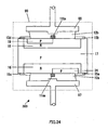
- FIGS. 26(a) and 26(b) are cross-sectional views showing a thyristor-type semiconductor device according to the related art, with FIG. 26(a) being a cross-sectional view of a thyristor-type semiconductor device in which electrode terminals have been correctly provided and FIG. 26(b) being a cross-sectional view of a thyristor-type semiconductor device in which one of the electrode terminals has been provided in a state where it is in contact with a silicon substrate.
- reference numeral 910 designates the semiconductor device
- reference numerals 912a, 912b, 912c designate solder
- reference numeral 913 designates a cathode terminal
- reference numerals 914, 921 designate anode terminals
- reference numerals 915a to 915d designate insulating films
- reference numeral 916 designates a first N-type layer
- reference numeral 917 designates a first P-type layer
- reference numeral 918 designates a second N-type layer
- reference numeral 919 designates a second P-type layer
- reference numeral 920 designates the silicon substrate.
- the semiconductor device 910 is formed with the first N-type layer 916, the first P-type layer 917, the second N-type layer 918, and the second P-type layer 919 being provided on top of one another within the silicon substrate 920.
- the second P-type layer 919 is formed inside the second N-type layer 918.
- the cathode terminal 913 is provided on the surface of the silicon substrate 920 on the same side as the first N-type layer 916, with the cathode terminal 913 being connected to the first N-type layer 916 by the solder 912a.
- the anode terminal 914 is provided on the surface of the silicon substrate 920 on the same side as the second N-type layer 918 and the second P-type layer 919, with the anode terminal 914 being connected to the second N-type layer 918 and the second P-type layer 919 by the solder 912b.
- insulating films 915a, 915c and insulating films 915b and 915d which are each formed of a glass material, are respectively provided at the boundary between the first N-type layer 916 and the first P-type layer 917 and in the periphery of this boundary and at the boundary between the second N-type layer 918 and the first P-type layer 917 and in the periphery of this boundary.
- the first P-type layer 917 is also connected to a gate electrode (not shown in the drawings). It should be noted that certain types of thyristor have a structure that does not include a gate electrode.
- the solder 912a is printed on one surface of the silicon substrate 920 and the solder 912b is printed on the other surface of the silicon substrate 920.
- the cathode terminal 913 is mounted on the solder 912a and the anode terminal 914 is mounted on the solder 912b.
- the silicon substrate 920 is placed in a reflow furnace and the solder 912a and the solder 912b are melted to respectively attach the cathode terminal 913 and the anode terminal 914.
- the cathode terminal 913 and the anode terminal 914 on the solder 912a, 912b there are cases, however, where during the mounting of the cathode terminal 913 and the anode terminal 914 on the solder 912a, 912b, one or both of the electrode terminals is mounted in a position that is displaced in one direction or the other. If the solder 912a, 912b is melted in the reflow furnace with one or both electrode terminals in a displaced state, as shown in FIG. 26(b) for example, the anode terminal 921 may be tilted and may be attached by the solder 912b, 912c in this tilted state.
- the cathode terminal 913 or the anode terminal 914 is in contact with the silicon substrate 920 in a tilted state, there are problems such as the flow of the electrical current becoming unbalanced.
- the semiconductor device 910 is mounted on a circuit board or the like, bad connections may occur between the tilted electrode terminal and the circuit board or the like.
- This type of problem can be remedied by accurately mounting the cathode terminal 913 and the anode terminal 914 on the solder 912a, 912b, though costly manufacturing equipment is required to do so, which pushes up the manufacturing cost of semiconductor devices.
- the semiconductor device 910 is a large-sized semiconductor device that handles a large current, due to the effects of warping and undulations in the silicon substrate 920, there are cases where the cathode terminal 913 or the anode terminal 914 comes into contact with the silicon substrate 920. In such cases also, problems occur, such as the flow of electrical current becoming unbalanced. When the semiconductor device 910 is mounted onto a circuit board or the like, this can also cause bad connections between the tilted electrode terminal and the circuit board or the like.
- a semiconductor device includes: a plurality of regions that are electrically isolated from one another on one surface of a semiconductor substrate; and a support that projects from the surface on an element isolating region for electrically isolating the plurality of regions and a conductive material that is provided on a upper surface of the semiconductor substrate; and an electrode terminal that is provided on the conductive material, wherein a support that projects from the surface is provided on the element isolating region.
- the support positioned below the electrode terminal supports the electrode terminal, so that the tilting of the electrode terminal can be suppressed to within a predetermined range. Even if there are warping and undulations in the semiconductor substrate, the electrode terminal can be effectively prevented from being provided in contact with the silicon substrate. Since little current flows in the element isolating region, the obstruction of the flow of current by the support can be very effectively suppressed.
- a power control semiconductor device comprising a plurality of wells that are provided on one surface of a semiconductor substrate; an insulated gate transistor that includes an insulated gate formed so as to straddle the plurality of wells and a channel forming region positioned under the insulated gate near a surface the well, and performs switching for a current flowing through the cannel forming region in a thickness direction of the semiconductor substrate; a conductive material that is provided on a upper surface of the semiconductor substrate; and an electrode terminal that is provided on the conductive material, wherein a support is provided on a gate electrode of the insulated gate transistor via an insulating firm and another support is also provided on the well.
- the supports positioned below the electrode terminal support the electrode terminal, so that the tilting of the electrode terminal can be suppressed to within a predetermined range. Even if there are warping and undulations in the semiconductor substrate, the electrode terminal can be effectively prevented from being provided in contact with the silicon substrate. Since little current flows in an insulated gate transistor, the obstruction of the flow of current by the support can be very effectively suppressed. Also, since the well which composes an insulated gate transistor has a relatively large area, by forming the support in a part of the well where little current flows, the obstruction of the flow of current by the support can be very effectively suppressed.
- FIGS. 1(a) and 1(b) are explanatory views showing the semiconductor device according to the first embodiment of the present invention, with FIG. 1(a) being a planar view of the semiconductor device and FIG. 1(b) being a cross-sectional view of the semiconductor device taken along the line A-A.
- the semiconductor device 110 of the present invention is a three-terminal reverse blocking thyristor.
- reference numeral 110 designates the semiconductor device
- reference numerals 11a, 11b designate supports
- reference numerals 12a, 12b designate solder
- reference numeral 13 designates a cathode terminal
- reference numeral 14 designates an anode terminal
- reference numerals 15a to 15d designate insulating films
- reference numeral 16 designates a first N-type layer
- reference numeral 17 designates a first P-type layer
- reference numeral 18 designates a second N-type layer
- reference numeral 19 designates a second P-type layer
- reference numeral 20 designates a silicon substrate
- reference numeral 21 designates a PN junction peripheral part
- reference numeral 22 designates a side surface.
- solder 12b the anode terminal 14
- the insulating films 15b, 15d have not been illustrated in FIG. 1(a) .
- the electrode terminals, solder, and insulating films have been omitted as necessary.
- the semiconductor device 110 is produced with the first N-type layer 16, the second N-type layer 18, and the second P-type layer 19 being formed inside the P-type silicon substrate 20.
- the remaining part in which these three layers are not formed composes the first P-type layer 17.
- the first N-type layer 16 is formed by doping the silicon substrate 20 with an N-type impurity, with the first N-type layer 16 extending from a second surface (the bottom surface in FIG. 1(b) ) of the silicon substrate 20 towards the inside.
- the first P-type layer 17 is exposed at the edges of the two main surfaces of the silicon substrate 20 and to the side surfaces of the silicon substrate 20, and is in contact with the first N-type layer 16 and the second N-type layer 18.
- the first P-type layer 17 is also connected to a gate electrode that has not been illustrated.
- the second N-type layer 18 is also formed by doping the silicon substrate 20 with an N-type impurity, and extends from a first surface of the silicon substrate 20, which is to say the opposite surface to the second surface where the first N-type layer 16 is formed, towards the inside. It should be noted that depending on how the semiconductor device 110 is used, a plurality of gate electrodes may be provided, or conversely, the semiconductor device 110 may not be provided with a gate electrode.
- the second P-type layer 19 formed inside the second N-type layer 18, is off-centered so as to be positioned close to the side surface 22 of the semiconductor device 110, and extends from the first surface of the silicon substrate 20 towards the inside. Also, as shown in FIG. 1(a) , the second N-type layer 18 and the second P-type layer 19 are formed in the shape of rectangles, with the first N-type layer 16 (not shown in FIG. 1(a) ) also being in the shape of a rectangle.
- the first N-type layer 16, the first P-type layer 17, the second N-type layer 18, and the second P-type layer 19 are formed one on top of the other and so form a PNPN junction. It should be noted that the first N-type layer 16, the first P-type layer 17, the second N-type layer 18, and the second P-type layer 19 do not need to be formed as rectangles, and may be formed in other shapes, such as ovals.
- the support 11 b, the solder 12b, the anode terminal 14, and the insulating films 15b, 15d are formed on the first surface of the silicon substrate 20.
- the support 11b is formed of a glass material, and is disposed on a part of the boundary between the second N-type layer 18 and the second P-type layer 19 that is opposite the side surface 22.
- the solder 12b is formed substantially flat in a region in which the second N-type layer 18 is formed so as to cover the support 11 b.
- the support 11 b is formed higher (thicker) than the insulating films 15b, 15d. As will be described later, to prevent the anode terminal 14 from tilting and coming into contact with the silicon substrate 20, it is preferable to make the support 11 b high (thick) enough to support the anode terminal 14 from below, which is to say, higher (thicker) than the insulating films 15b, 15d.
- the support 11 b is formed thinner (lower) than the solder 12b, and preferably should be formed slightly lower than the solder 12b. This is because it is preferable for the support 11 b that projects from the lower surface of the solder 12b not to obstruct the attachment of the solder 12b to the anode terminal 14.
- the anode terminal 14 is formed on the solder 12b and is electrically connected to the second N-type layer 18 and the second P-type layer 19 via the solder 12b.
- the insulating film 15b is formed of a glass material, and covers the part of the boundary between the first P-type layer 17 and the second N-type layer 18 that is opposite the side surface 22 and the periphery of this part, thereby protecting the covered parts.
- the insulating film 15d is also formed of a glass material, and covers the side surface 22 side parts of (i) the boundary of the first P-type layer 17 and the second N-type layer 18 and (ii) the boundary between the second N-type layer 18 and the second P-type layer 19, as well as the peripheries of these parts, thereby protecting the covered parts.
- the support 11a, the solder 12a, the cathode terminal 13, and the insulating films 15a, 15c are provided on the second surface of the silicon substrate 20.
- the support 11a is formed of a glass material and is disposed substantially centrally in a surface region of the first N-type layer 16.
- the support 11 a is formed higher (thicker) than the insulating films 15a, 15c. As will be described later, to prevent the cathode terminal 13 from tilting and coming into contact with the silicon substrate 20, it is preferable to make the support 11 a high (thick) enough to support the cathode terminal 13 from below, which is to say, higher (thicker) than the insulating films 15a, 15c.
- the support 11 a is formed thinner (lower) than the solder 12a, and preferably should be formed slightly lower than the solder 12a. This is because it is preferable for the support 11a that projects from the upper surface of the solder 12a not to obstruct the attachment of the solder 12a to the cathode terminal 13.
- the solder 12a is formed substantially flat in a region in which the first N-type layer 16 is formed so as to cover the support 11a. It should be noted that when the solder 12a is provided by printing it onto the surface of the silicon substrate 20, the support 11 a is produced with a thickness that allows the support 11 a to be hidden within the solder 12a for the reasons given above.
- the cathode terminal 13 is formed on the solder 12a and is electrically connected to the first N-type layer 16 via the solder 12a.
- the insulating films 15a, 15c are formed of a glass material, and cover the boundary between the first N-type layer 16 and the first P-type layer 17 and the periphery of this boundary, thereby protecting these parts. It should be noted that the insulating films 15a, 15c and the insulating films 15b, 15d may be formed of another insulating material, such as silicon oxide (Si02), instead of a glass material.
- this current flows from the solder 12b to the second N-type layer 18, but as time passes, the current that flows from the solder 12b to the second N-type layer 18 via the second P-type layer 19 increases. Since the second P-type layer 19 is provided off-center towards the side surface 22, when the majority of the current flows via the second P-type layer 19, such flow is concentrated in the center of the second P-type layer 19, and hardly any current flows at the PN junction peripheral part 21 near the interface between the second N-type layer 18 and the second P-type layer 19. Accordingly, when the semiconductor device 110 is turned on, the supports 11 a, 11 b do not obstruct the flow of current.
- the following is an overview of the procedure that provides the cathode terminal 13 and the anode terminal 14 on the silicon substrate 20.
- the supports 11a, 11 b and the solder 12a, 12b are provided in advance on the surfaces of the silicon substrate 20.
- the cathode terminal 13 is mounted on the solder 12a and the anode terminal 14 is mounted on the solder 12b.
- the silicon substrate 20 is placed in a reflow furnace, and the cathode terminal 13 and the anode terminal 14 are attached by melting the solder 12a, 12b.
- the supports 11 a, 11 b are provided in advance, with the supports 11 a, 11 b supporting the electrode terminals from below and thereby preventing the electrode terminals from tilting significantly and so coming into contact with the silicon substrate 20.
- the semiconductor device 110 is provided with supports 11a, 11b so that when the cathode terminal 13 and the anode terminal 14 are provided on the silicon substrate 20, these electrode terminals can be prevented from being provided in a state where the electrode terminals are significantly tilted and contact the silicon substrate 20.
- the supports 11a, 11b are provided at positions on the surface of the silicon substrate 20 where is difficult for current to flow, so that when the semiconductor device 110 is turned on, the supports 11a, 11b do not obstruct the flow of current.
- the supports 11a, 11b can be formed of the same material and with the same height (thickness) as the insulating films 15a, 15c and the insulating films 15b, 15d.
- the supports 11a, 11b, the insulating films 15a, 15c and the insulating films 15b, 15d can be provided by the same process, so that there is no need for a special process for providing the supports 11a, 11b.
- electrode terminals that are not plate-like such as plate-like electrode terminals that have a cylindrical body provided on one side, may be used in place of plate-like electrode terminals.
- FIGS. 2(a) to 2(c) a method of manufacturing the semiconductor device 110 according to the first embodiment of the present invention.
- the semiconductor device 110 according to the first embodiment is manufactured by the following processes.
- a semiconductor device that has (1) the second N-type layer 18 that is formed by exposing one surface of the silicon substrate 20, (2) the second P-type layer 19 that is formed inside the second P-type layer 19 when exposing this surface of the silicon substrate 20, and (3) the first N-type layer 16 that is formed by exposing the other surface of the silicon substrate 20, is manufactured (not illustrated).
- the insulating films 15b, 15d are formed at the boundary of the second N-type layer 18 or the periphery of this boundary and the insulating films 15a, 15c are formed at the boundary of the first N-type layer 16 or the periphery of this boundary (see FIG. 2(a) ).
- the support 11 b is formed so as to project from the surface of the silicon substrate 20 at the boundary between the second N-type layer 18 and the second P-type layer 19 or at the periphery of this boundary, with the upper end of the support 11 b being higher than the upper ends of the insulating films 15b, 15d.
- the support 11 a is formed so as to project from the surface of the first N-type layer 16, with the upper end of the support 11 a being higher than the upper ends of the insulating films 15a, 15c (see FIG. 2(b) ).
- the supports 11b, 11a are manufactured by coating the semiconductor device (main body) with a resist that includes a glass material using a metal mask. After this, the entire semiconductor device (main body) is calcinated, and the resist, in which a pattern has been formed, is converted into glass.
- solder 12b is applied on the second N-type layer 18 and the second P-type layer 19 as a conductive material that is thicker than the support 11b, and the solder 12a is applied onto the first N-type layer 16 of the semiconductor device so as to be thicker than the support 11 a (not illustrated).
- the semiconductor device 110 according to the first embodiment of the present invention is manufactured by performing the above manufacturing processes.
- This method of manufacturing a semiconductor device according to the first embodiment can manufacture a semiconductor device with the superior effects described above in a relatively simple manner where a support forming process is additionally performed after the insulating film forming process.
- FIGS. 3(a) to 3(c) a method of manufacturing a semiconductor device 120 according to a second embodiment of the present invention is described using FIGS. 3(a) to 3(c) .
- the semiconductor device 120 according to the second embodiment is manufactured by the following processes.
- the semiconductor device (main body) is manufactured in the same way as in the first embodiment (not illustrated).
- the insulating films 15b, 15d, 30b are formed at the boundary of the second N-type layer 18 or the periphery of this boundary and at the boundary between the second N-type layer 18 and the second P-type layer 19 or the periphery of this boundary.
- the insulating films 15a, 15c, 30a are formed at the boundary of the first N-type layer 16 or the periphery of this boundary and additionally in a central part of the first N-type layer 16 (see FIG. 3(a) ).
- a glass layer 31 b is formed on the insulating film formed at the boundary between the second N-type layer 18 and the second P-type layer 19 or the periphery of this boundary according to the same method as in the first embodiment, and this glass layer 31b is set as the support 11b2.
- a glass layer 31 a is formed on the insulating film 31 a formed in the center of the first N-type layer 16 and is set as the support 11 a2 (see FIG. 3(b) ).
- solder 12b is applied on the second N-type layer 18 and the second P-type layer 19 of the semiconductor device so as to be thicker than the support 11b2, and the solder 12a is applied onto the first N-type layer 16 of the semiconductor device so as to be thicker than the support 11 a2 (not illustrated).
- the semiconductor device 120 according to the second embodiment of the present invention is manufactured by performing the above manufacturing processes.
- This method of manufacturing a semiconductor device according to the second embodiment realizes the same effects as the method of manufacturing according to the first embodiment of the present invention, with there being a further effect in that it is possible to manufacture the supports 11 b2, 11 a2 with a structure that is resistant to thermal stress.
- FIGS. 4(a) to 4(d) a method of manufacturing a semiconductor device 130 according to a third embodiment of the present invention is described using FIGS. 4(a) to 4(d) .
- the semiconductor device 130 according to the third embodiment is manufactured by the following processes.
- the semiconductor device (main body) is manufactured in the same way as in the first embodiment (not illustrated).
- the insulating films 15b, 15d are formed at the boundary of the second N-type layer 18 or the periphery of this boundary and the insulating films 15a, 15c are formed at the boundary of the first N-type layer 16 or the periphery of this boundary (see FIG. 4(a) ).
- a layer 32b of adhesive is formed at the boundary between the second N-type layer 18 and the second P-type layer 19 or at the periphery of this boundary (see FIG. 4(b) ).
- a glass layer 33b is formed on this layer 32b and is set as the support 11b3 (see FIG. 4(c) ).
- a layer 32a of adhesive is formed in a central part of the first N-type layer 16 (see FIG. 4(b) ), and a glass layer 33a is formed on this layer 32a and is set as the support 11 a3 (see FIG. 4(c) ).
- solder 12b is applied on the second N-type layer 18 and the second P-type layer 19 of the semiconductor device so as to be thicker than the support 11 b3, and the solder 12a is applied onto the first N-type layer 16 of the semiconductor device so as to be thicker than the support 11 a3 (not illustrated).
- the semiconductor device 130 according to the third embodiment of the present invention is manufactured by performing the above manufacturing processes.
- This method of manufacturing a semiconductor device according to the third embodiment realizes the same effects as the method of manufacturing according the first embodiment of the present invention, with there being a further effect of the ease with which supports can be formed on a semiconductor device with a relatively large area.
- FIGS. 5(a) to 5(d) a method of manufacturing a semiconductor device 140 according to a fourth embodiment of the present invention is described using FIGS. 5(a) to 5(d) .
- the semiconductor device 140 according to the fourth embodiment is manufactured by the following processes.
- the semiconductor device (main body) is manufactured in the same way as in the first embodiment (not illustrated).
- a thick insulating film 34b is formed on one entire surface of the semiconductor device (main body) and a thick insulating film 34a is formed on another entire surface of the semiconductor device (main body) (see FIG. 5(a) ).
- etching is performed so as to leave the thick insulating film 34b at desired positions, thereby forming thick insulating films 35b, 35d, 11 b4 at the boundary of the second N-type layer 18 or at the periphery of this boundary and at the boundary between the second N-type layer 18 and the second P-type layer 19 or at the periphery of this boundary (see FIG. 5(b) ).
- etching is performed so as to leave the thick insulating film 34a at desired positions, thereby forming thick insulating films 35a, 35c, 11 a4 at the boundary of the first N-type layer 16 or the periphery of this boundary and at a central part of the first N-type layer 16 (see FIG. 5(b) ).
- the thick insulating films 35b, 35d, 35a, and 35c may be left as they are, or only these parts may be subjected to selective etching to reduce the thickness of the films, thereby converting the thick insulating films into the insulating films 15b, 15d, 15a, 15c that are in the form of thin films (see FIG. 5(c) ).
- solder 12b is applied on the second N-type layer 18 and the second P-type layer 19 of the semiconductor device so as to be thicker than the support 11 b4, and the solder 12a is applied onto the first N-type layer 16 of the semiconductor device so as to be thicker than the support 11 a4 (not illustrated).
- the semiconductor device 140 according to the fourth embodiment of the present invention is manufactured by performing the above manufacturing processes.
- This method of manufacturing a semiconductor device according to the fourth embodiment realizes the same effects as the method of manufacturing according the first embodiment of the present invention, with there being a further effect in that the insulating films and supports can be produced at the same time.
- FIG. 6 is a planar view showing the semiconductor device 150 according to the fifth embodiment of the present invention.
- the semiconductor device 150 has a support 11 b5 provided in a side part of an internal region of the second P-type layer 19. It should be noted that the support 11 b5 in this fifth embodiment is provided in a periphery of a part of the boundary between the second N-type layer 18 and the second P-type layer 19 that is opposite the side surface 22 so as to minimize the effects on the flow of current when the semiconductor device 150 is turned on.
- FIG. 7 is a planar view showing the semiconductor device 160 according to the sixth embodiment of the present invention.
- the semiconductor device 160 has a support 11 b6 provided in a side part of an internal region of the second N-type layer 18. It should be noted that the support 11 b6 in this sixth embodiment is provided in a periphery of a part of the boundary between the second N-type layer 18 and the second P-type layer 19 that is opposite the side surface 22 so as to minimize the effects on the flow of current when the semiconductor device 160 is turned on.
- the semiconductor devices 150, 160 have the supports 11b5, 11 b6 formed at positions that are not on the boundary between the second N-type layer 18 and the second P-type layer 19, so that while there is a slightly larger effect on the current when the semiconductor devices 150, 160 are turned on compared to the semiconductor device 110 of the first embodiment of the present invention, the supports can be positioned with greater freedom. Accordingly, the positions of the supports can be appropriately set for various conditions, such as the size of the anode terminal 14.
- FIG. 8 is a cross-sectional view showing the semiconductor device 170 according to the seventh embodiment of the present invention.
- the reference numerals used in this drawing are the same as those in FIGS. 1(a) and 1(b) .
- reference numerals 23a, 23b designate supports, and the other reference numerals designate the same parts as in FIG. 1 .
- the supports 23a, 23b are provided on the cathode terminal 13 and the anode terminal 14 respectively, not on the surfaces of the silicon substrate 20. It should be noted that it is preferable for the heights of the supports 23a, 23b to be set using the same conditions as the supports 11 a, 11 b.
- the supports 23a, 23b are respectively provided on the surfaces of the cathode terminal 13 and the anode terminal 14 that face the silicon substrate 20, so that when the cathode terminal 13 and the anode terminal 14 are provided, even if the cathode terminal 13 and the anode terminal 14 are tilted, the supports 23a, 23b contact the surfaces of the silicon substrate 20 and so prevent the electrode terminals from tilting by a predetermined amount or more.
- the same effects as the semiconductor device according to the first embodiment of the present invention can be obtained without modifying the processes that provide the solder 12a, 12b and the insulating films 15a to 15d.
- the supports are described as being in the form of rectangular solids, though the supports may be formed in other shapes, such as cylinders or hemispheres. Also, while the provision of one support for each of the cathode terminal and the anode terminal has been described, so long as the flow of current is not obstructed when the semiconductor device is turned on, it is preferable to provide a plurality, such as two, three, or four, supports for one or both of the electrode terminals to reliably prevent tilting of the electrode terminals.
- thyristor-type semiconductor devices are described as examples, though the present invention may be applied to other types of semiconductor device, such as a triac, where it is possible to form a support on a PN junction.
- FIGS. 9(a) and 9(b) show the semiconductor device 180 according to the eighth embodiment of the present invention, with FIG. 9(a) being a planar view of the semiconductor device 180 and FIG. 9(b) being a cross-sectional view of the semiconductor device 180 taken along the line A-A.
- the semiconductor device 180 according to this eighth embodiment differs from the semiconductor device 110 according to the first embodiment in the structure of the second surface. This is to say, while the first N-type layer 16 is provided on the second surface of the semiconductor device 110 according to the first embodiment, the first N-type layer 16 and a third P-type layer 24 that is formed inside the first N-type layer 16 are provided on the second surface of the semiconductor device 180 according to the eighth embodiment. In this way, the semiconductor device 180 according to the eighth embodiment is a bidirectional thyristor.
- the semiconductor device 180 according to the eighth embodiment has the same structure as the first surface of the semiconductor device 110 according to the first embodiment on both the first and second surfaces, and so obtains the same effects has the semiconductor device 180 according to the first embodiment.
- FIGS. 10(a) and 10(b) show the semiconductor device 190 according to the ninth embodiment of the present invention, with FIG. 10(a) being a planar view of the semiconductor device 190 and FIG. 10(b) being a cross-sectional view of the semiconductor device 190 taken along the line A-A.
- the semiconductor device 190 according to this ninth embodiment differs from the semiconductor device 180 according to the eighth embodiment in the number of thyristors included in the semiconductor device. This is to say, while the semiconductor device 180 according to the eighth embodiment includes one bidirectional thyristor, the semiconductor device 190 according to the ninth embodiment includes two bidirectional thyristors.
- two second N-type layers 18 are formed on one surface and a second P-type layer 19 is formed inside each of these two second N-type layers 18.
- a support 11 b9 is formed in a region that faces the two second N-type layers 18. There is fundamentally little flow of current in this region that faces the two second N-type layers 18, so that the semiconductor device 190 has a structure where the obstruction of the flow of current by the support 11 b9 is very effectively suppressed.
- FIGS. 11 (a) and 11 (b) show the semiconductor device 200 according to the tenth embodiment of the present invention, with FIG. 11(a) being a planar view of the semiconductor device 200 and FIG. 11 (b) being a cross-sectional view of the semiconductor device 200 taken along the line A-A.
- the semiconductor device 200 according to the tenth embodiment differs from the semiconductor device 190 according to the ninth embodiment in the number of anode terminals 14. This is to say, while the semiconductor device 180 according to the ninth embodiment includes one anode terminal 14, the semiconductor device 200 according to the tenth embodiment includes two anode terminals 14.
- two supports 11b10 are formed in a region that faces the two second N-type layers 18. There is fundamentally little flow of current in this region that faces the two second N-type layers 18, so that the semiconductor device 200 has a structure where the obstruction of the flow of current by the supports 11b10 is very effectively suppressed.
- FIG. 12 is a cross-sectional view showing the semiconductor device 210 according to the eleventh embodiment of the present invention and FIGS. 13(a) and 13(b) are planar views showing the semiconductor device 210 according to the tenth embodiment of the present invention.
- FIG. 13(a) is a planar view showing one surface (the first surface) of the semiconductor device 210 and FIG. 13(b) is a planar view showing another surface (the second surface) of the semiconductor device 210.
- the semiconductor device 210 according to the eleventh embodiment differs from the semiconductor device 110 according to the first embodiment in the position at which the second P-type layer 19 is formed on the first surface and in the number and positions of the supports 11b11. While the second P-type layer 19 is formed off-center towards the side surface 22 of the semiconductor device 110 according to the first embodiment, the second P-type layer 19 in the semiconductor device 210 according to the eleventh embodiment is formed in a central part of the second N-type layer 18 formed in the semiconductor device 210.
- supports 11b11 in the semiconductor device 210 according to the eleventh embodiment are formed at four positions in a peripheral part of the second P-type layer 19.
- supports 11a11 are formed at four positions in a boundary part between the first N-type layer 16 and a fourth P-type layer 36 formed in the peripheral part of the first N-type layer 16.
- the supports 11b11, 11a11 are formed as cylinders. Accordingly, the creation of voids can be effectively suppressed during the reflow process.
- FIGS. 14(a) and 14(b) are planar views showing the semiconductor device 220 according to the twelfth embodiment of the present invention.
- FIG. 14(a) is a planar view showing one surface (the first surface) of the semiconductor device 220 and
- FIG. 13(b) is a planar view showing another surface (the second surface) of the semiconductor device 220.
- the semiconductor device 220 according to the twelfth embodiment differs from the semiconductor device 210 according to the eleventh embodiment in the number of supports. While four supports are formed on each surface of the semiconductor device 110 according to the eleventh embodiment, three supports are formed on each surface of the semiconductor device 220 according to the twelfth embodiment.
- FIG. 15 is a cross-sectional view of the semiconductor device 230 according to the thirteenth embodiment of the present invention
- FIG. 16 is a planar view showing one surface (the first surface) of the semiconductor device 230
- FIG. 17 is a planar view showing another surface (the second surface) of the semiconductor device 230.
- the conductivity of the substrate in the semiconductor device 230 according to the thirteenth embodiment is the reverse of that in the semiconductor device 110 according to the first embodiment.
- the semiconductor device 230 according to the thirteenth embodiment differs from the semiconductor device 110 according to the first embodiment in the positions at which the supports are formed. This is to say, while the support 11 b is formed at the boundary between the second N-type layer 18 and the second P-type layer 19 in the semiconductor device 110 according to the first embodiment, a plurality of supports 11b13 are formed at positions in a peripheral part of the second P-type layer 119 in the semiconductor device 230 according to the thirteenth embodiment. One of these supports is formed at a position on the second P-type layer 119 that faces a region 137 for providing a potential to the gate.
- the supports 11b13 are formed at different positions in the semiconductor device 230 according to the thirteenth embodiment to the semiconductor device 110 according to the first embodiment. Since there is little flow of current at these parts also, the obstruction of the flow of current by the supports 11b13 is very effectively suppressed.
- a plurality of supports 11a13 are formed at positions around a peripheral part of the third P-type layer 138 that is formed in the first P-type layer 116. In this way, the supports 11a13 are formed at different positions in the semiconductor device 230 according to the thirteenth embodiment to the semiconductor device 110 according to the first embodiment. Since there is little flow of current at these parts also, the obstruction of the flow of current by the supports 11a13 is very effectively suppressed.
- a support is shown by the reference numeral (11a13') in FIG. 17 .
- supports which are formed with a small area so as to hardly obstruct the flow of current can be disposed in the third P-type layer 138.
- two supports 11c are also formed in a region 137 that supplies potential to the gate (see FIG. 16 ).
- FIG. 18 is a cross-sectional view of the semiconductor device 240 according to the fourteenth embodiment of the present invention.
- the semiconductor device 240 according to the fourteenth embodiment differs from the semiconductor device 230 according to the thirteenth embodiment in the position at which the region 137 for supplying the gate potential is formed. While the region 137 for supplying the gate potential is formed in a peripheral part of the semiconductor device 230 according to the thirteenth embodiment, the region 137 for supplying the gate potential is formed in a central part of the semiconductor device 240 according to the fourteenth embodiment.
- the region 137 for supplying the gate potential is formed at a different position in the semiconductor device 240 according to the fourteenth embodiment to the semiconductor device 230 according to the thirteenth embodiment, though in this case also, the supports 11b14 are formed at a boundary part between the region 137 for supplying the gate potential and the second N-type layers 119, which is to say at a part where there is little flow of current, so that the obstruction of the flow of current by the supports is very effectively suppressed.
- FIG. 19 is a cross-sectional view of the semiconductor device 250 according to the fifteenth embodiment of the present invention.
- the semiconductor device 250 has a plurality of regions that are electrically isolated on one surface of the semiconductor device 250.
- the semiconductor device 250 is characterized by having a support 51 provided on an element isolating region 44 that electrically isolates the plurality of regions.
- an electrode terminal 50 When an electrode terminal 50 is connected to a conductive region of the semiconductor substrate via a conductive member 49, even if the electrode terminal 50 is displaced and tilted, a support 51 positioned below the electrode terminal 50 supports the electrode terminal 50, so that the tilting of the electrode terminal 50 can be suppressed to within a predetermined range. Even if there are warping and undulations in the silicon substrate, the electrode terminal 50 can be effectively prevented from being provided in a state where the electrode terminal 50 is in contact with the silicon substrate. Since little current flows on the element isolating region 44, the support 51 does not obstruct the flow of current.
- FIG. 20 is a cross-sectional view of the semiconductor device 260 according to the sixteenth embodiment of the present invention.
- the semiconductor device 260 according to the sixteenth embodiment has fundamentally the same structure as the semiconductor device 250 according to the fifteenth embodiment.
- the semiconductor device 260 according to the sixteenth embodiment differs from the semiconductor device 250 according to the fifteenth embodiment in the structure of the element isolating construction.
- the element isolating structure in the semiconductor device 250 according to the fifteenth embodiment is the element isolating region 44 that is realized by a PN junction
- the element isolating structure in the semiconductor device 260 according to the sixteenth embodiment is an element isolating structure 58 that is realized by burying a Si02 insulating film as far as the Si02 insulating layer 55 that is the I (Insulator) layer in an SOI (Silicon On Insulator) structure.
- the semiconductor device 260 according to the sixteenth embodiment of the present invention is similar to the semiconductor device 250 according to the fifteenth embodiment in that the support 65 is formed on the element isolating structure 58, so that the same effects are obtained as in the fifteenth embodiment.
- FIG. 21 is a cross-sectional view of the semiconductor device 270 according to the seventeenth embodiment of the present invention.
- the semiconductor device 270 according to the seventeenth embodiment is a power control semiconductor device with an insulated gate transistor, which switches a current flowing in the thickness direction of the semiconductor device, formed on one surface of the semiconductor substrate.
- a support 72 is provided on a gate electrode 71 of the insulated gate transistor via an insulating film, and by providing supports 73 on the P wells 67, 68 in which source regions 69, 70 are formed, the following effects can be obtained.
- the supports 72, 73 positioned below the electrode terminal 76 support the electrode terminal 76, so that the tilting of the electrode terminal 76 can be suppressed to within a predetermined range. Also, even if there are warping and undulations in the silicon substrate, the electrode terminal 76 can be effectively prevented from being provided in a state where the electrode terminal 76 is in contact with the silicon substrate. Since little current flows at an insulated gate transistor, the support 72 does not obstruct the flow of current.
- the P wells 67, 68 each have a relatively large area, and by forming the supports 73 in parts of the P wells 67, 68 where little current flows, the supports 73 can be prevented from obstructing the flow of current.
- the supports 73 are provided on P wells, though if there is a region where there is little flow of current, the supports 73 may be favorably provided in such region instead. As one example, the supports 73 may be provided on a non-active region of the semiconductor substrate.
- the support 77 positioned below the electrode terminal 79 supports the electrode terminal 79, so that the tilting of the electrode terminal 79 can be suppressed to within a predetermined range. Even if there are warping and undulations in the silicon substrate, the electrode terminal 79 can be effectively prevented from being provided in a state where the electrode terminal 79 is in contact with the silicon substrate.
- FIG. 22 is a cross-sectional view of the semiconductor device 280 according to the eighteenth embodiment of the present invention.
- the semiconductor device 280 according to the eighteenth embodiment is a power control semiconductor device where a semiconductor substrate 80 is mounted on a printed circuit board 95.
- a drain electrode part 81 formed in the semiconductor substrate 80 is connected to a drain metal electrode 86 via a conductive adhesive 85.
- the drain metal electrode 86 is connected to a drain electrode part 88 of the printed circuit board 95 via solder 87.
- a source electrode part 82 formed in the semiconductor substrate 80 is connected to a source electrode part 93 of the printed circuit board 95 via solder 91.
- a gate electrode part 83 formed in the semiconductor substrate 80 is connected to a gate electrode part 94 of the printed circuit board 95 via solder 92.
- supports in FIG. 22 , supports 84 in a region in which the drain electrode part 81 is formed, a support 89 in a region in which the source electrode part 82 is formed, and a support 90 in a region in which the gate electrode part 83 is formed) are provided at positions where the flow of current on the semiconductor substrate 80 is not obstructed, so that the following effects are obtained.
- the presence of the supports 84, 89, 90 means that the tilting of the printed circuit board 95 and the semiconductor substrate 80 and the tilting of the semiconductor substrate 80 and the drain metal electrode 86 can be suppressed within predetermined ranges.
- the source electrode part 93 on the printed circuit board 95, the gate electrode part 94 on the printed circuit board 95, and the drain metal electrode 86 can be effectively prevented from being provided in a state where these parts are in contact with the semiconductor substrate 80.
- FIG. 23 is a cross-sectional view of the semiconductor device 290 according to the nineteenth embodiment of the present invention.
- the semiconductor device 290 according to the nineteenth embodiment is a power control semiconductor device 290 where the semiconductor substrate 80 is mounted on a printed circuit board 95.
- the semiconductor device 290 according to the nineteenth embodiment differs from the semiconductor device 280 according to the eighteenth embodiment in the structure of the support.
- the support 84 is formed so as to be thinner than the thickness of the conductive adhesive 85, and when as a result the drain metal electrode 86 is correctly set on the semiconductor substrate 80, the support 84 and the drain metal electrode 86 do not come into contact.
- the support 96 and the drain metal electrode 86 are always in contact.
- the support 96 functions as a spacer between the semiconductor substrate 80 and the drain metal electrode 86.
- the drain metal electrode 86 is provided so as to face one surface of the semiconductor substrate 80 with the support 96 in between as a spacer, so that when the reflow process is performed, there is the effect that the drain metal electrode 86 is not attached to the semiconductor substrate 80 in a tilted state.
- FIG. 24 is a cross-sectional view of the semiconductor device 300 according to the twentieth embodiment of the present invention.
- the semiconductor device 300 according to the twentieth embodiment resembles the semiconductor device 180 according to the eighth embodiment.
- the semiconductor device 300 according to the twentieth embodiment differs from the semiconductor device 180 according to the eighth embodiment in the structure of the electrode terminals. While the electrode terminals 13, 14 are in the form of flat plates in the semiconductor device 180 according to the eighth embodiment, electrode terminals 97, 98 in the semiconductor device 300 according to the twentieth embodiment have a convex part formed on an inner surface and also have lead wires attached to them.
- This semiconductor device 300 also realizes the same effects as the semiconductor device 180 according to the eighth embodiment.
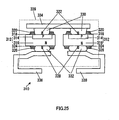
- FIG. 25 is a cross-sectional view of the semiconductor device 310 according to the twenty-first embodiment of the present invention.
- the semiconductor device 310 according to the twenty-first embodiment is a surface-mounted semiconductor device 310.
- two semiconductor substrates 312 which have a PN diode structure with a P-type region 314 formed in an N-type region 316, are connected in series with opposite orientations and are molded using a resin mold 339.
- P-type regions 314 of the two semiconductor substrates 312 are connected to each other via solder 330 and a metal electrode 334.
- N-type regions 316 of the two semiconductor substrates 312 are each connected via solder 332 to separate metal electrodes 336, 338, respectively.
- supports 322 are formed on the surfaces of the P-type regions 314 and supports 328 are formed on the surfaces of the N-type region 316. For this reason, when a reflow process is performed with the semiconductor substrates 312, the metal electrode 334, and the metal electrodes 336, 338 having been arranged with a predetermined positional relationship, even if the semiconductor substrates 312 and the metal electrode 334 are tilted, or if the semiconductor substrates 312 and the metal electrodes 336, 338 are tilted, the presence of the supports 322, 328 makes it possible to suppress the tilting of the semiconductor substrates 312 and the metal electrode 334 and the tilting of the semiconductor substrates 312 and the metal electrodes 336, 338 to within predetermined ranges.
- the metal electrodes 334, 336, 338 can be effectively prevented from being provided in a state where these parts are in contact with the silicon substrates 312.
- the electrode terminals can be attached using other conductive materials, such as conductive adhesive.
- conductive adhesive or the like is used, it is possible to absorb stress in the conductive material and to attach the electrode terminals at low temperatures.
- the supports may be attached to the silicon substrate using adhesive.
- a material whose thermal expansion coefficient is close to that of the silicon substrate as the glass material used for the supports with it also being preferable to use a material with favorable thermal shock resistance, firing temperature, electrical characteristics, electrical charge in glass, and adhesion.
- the supports may also be made from an environmentally-friendly material. As one example, lead-free glass may be used preferably.
- the present invention has supports provided on silicon substrates or electrode terminals, so that when electrode terminals are provided on a silicon substrate, the electrode terminals can be prevented from being provided in a state where the electrode terminals are in contact with the silicon substrate. Even if there are warping and undulations in the surface of the silicon substrate, the electrode terminal can be prevented from being provided in a state where the electrode terminal is in contact with the silicon substrate.
- the semiconductor device of the present invention has supports formed on the semiconductor substrate or on the electrode terminals, so that even when conventional manufacturing equipment is used to attach the electrode terminals, it is possible to prevent the electrode terminals from being attached to the semiconductor substrate in a significantly tilted state, with it also being possible to prevent the electrode terminals from being attached in a state where the electrode terminals are in contact with the semiconductor substrate, even when there are warping and undulations in the semiconductor substrate.
- the supports can be formed at positions (such as above a PN junction) where little current flows.
- power semiconductor devices that have a PN junction such as thyristors, triacs, diodes, MOSFETs, IGBTs and GTOs can be manufactured with a high yield with no loss in the performance of the semiconductor devices.
Landscapes
- Electrodes Of Semiconductors (AREA)
- Thyristors (AREA)
Applications Claiming Priority (2)
| Application Number | Priority Date | Filing Date | Title |
|---|---|---|---|
| JP2001138058 | 2001-05-09 | ||
| EP02769218A EP1387407B1 (fr) | 2001-05-09 | 2002-05-08 | Dispositif semi-conducteur et son procédé de fabrication |
Related Parent Applications (1)
| Application Number | Title | Priority Date | Filing Date |
|---|---|---|---|
| EP02769218A Division EP1387407B1 (fr) | 2001-05-09 | 2002-05-08 | Dispositif semi-conducteur et son procédé de fabrication |
Publications (2)
| Publication Number | Publication Date |
|---|---|
| EP1970962A1 true EP1970962A1 (fr) | 2008-09-17 |
| EP1970962B1 EP1970962B1 (fr) | 2015-01-21 |
Family
ID=18985056
Family Applications (2)
| Application Number | Title | Priority Date | Filing Date |
|---|---|---|---|
| EP02769218A Expired - Lifetime EP1387407B1 (fr) | 2001-05-09 | 2002-05-08 | Dispositif semi-conducteur et son procédé de fabrication |
| EP08003214.7A Expired - Lifetime EP1970962B1 (fr) | 2001-05-09 | 2002-05-08 | Dispositif semi-conducteur |
Family Applications Before (1)
| Application Number | Title | Priority Date | Filing Date |
|---|---|---|---|
| EP02769218A Expired - Lifetime EP1387407B1 (fr) | 2001-05-09 | 2002-05-08 | Dispositif semi-conducteur et son procédé de fabrication |
Country Status (6)
| Country | Link |
|---|---|
| US (1) | US7125754B2 (fr) |
| EP (2) | EP1387407B1 (fr) |
| JP (1) | JP4035447B2 (fr) |
| CN (1) | CN1271723C (fr) |
| BR (1) | BR0205106A (fr) |
| WO (1) | WO2002091474A1 (fr) |
Families Citing this family (6)
| Publication number | Priority date | Publication date | Assignee | Title |
|---|---|---|---|---|
| US7863727B2 (en) * | 2006-02-06 | 2011-01-04 | Micron Technology, Inc. | Microelectronic devices and methods for manufacturing microelectronic devices |
| KR100869795B1 (ko) * | 2006-11-02 | 2008-11-21 | 삼성에스디아이 주식회사 | 플라즈마 표시 장치 및 그 구동 방법 |
| CN101807598B (zh) * | 2010-03-17 | 2011-12-14 | 浙江大学 | 一种pnpnp型双向可控硅 |
| CN103730534B (zh) * | 2013-12-16 | 2016-06-15 | 启东吉莱电子有限公司 | 一种高压双向触发器件及其制作方法 |
| US9455253B2 (en) * | 2014-07-23 | 2016-09-27 | Stmicroelectronics (Tours) Sas | Bidirectional switch |
| CN107611087B (zh) * | 2017-08-30 | 2020-07-17 | 常州银河世纪微电子股份有限公司 | 单向放电管的制作方法 |
Citations (7)
| Publication number | Priority date | Publication date | Assignee | Title |
|---|---|---|---|---|
| EP0099175A2 (fr) * | 1982-06-21 | 1984-01-25 | Eaton Corporation | Transistor à effet de champ comportant une électrode de porte sous-divisée |
| US4746625A (en) * | 1986-06-09 | 1988-05-24 | Kabushiki Kaisha Toshiba | A method of manufacturing semiconductor elements-isolating silicon oxide layers |
| US4847671A (en) * | 1987-05-19 | 1989-07-11 | General Electric Company | Monolithically integrated insulated gate semiconductor device |
| EP0590804A1 (fr) * | 1992-09-03 | 1994-04-06 | STMicroelectronics, Inc. | Transistor bipolaire monolithique à haute puissance verticalement isolé avec un collecteur de dessus |
| US5796123A (en) | 1995-11-30 | 1998-08-18 | Sgs-Thomson Microelectronics S.A. | Semiconductor component mounted by brazing |
| US5898806A (en) * | 1991-11-07 | 1999-04-27 | Nec Corporation | Optical interconnection circuit structure |
| EP1143519A2 (fr) * | 2000-04-04 | 2001-10-10 | Lucent Technologies Inc. | Appareil et procédé pour l'assemblage de dispositifs optiques |
Family Cites Families (14)
| Publication number | Priority date | Publication date | Assignee | Title |
|---|---|---|---|---|
| JP2642548B2 (ja) * | 1991-09-26 | 1997-08-20 | 株式会社東芝 | 半導体装置およびその製造方法 |
| JPH05267362A (ja) * | 1992-03-19 | 1993-10-15 | Hitachi Ltd | 半導体装置の実装構造 |
| US5422289A (en) * | 1992-04-27 | 1995-06-06 | National Semiconductor Corporation | Method of manufacturing a fully planarized MOSFET and resulting structure |
| US5319222A (en) * | 1992-04-29 | 1994-06-07 | North Carolina State University | MOS gated thyristor having on-state current saturation capability |
| JPH05343658A (ja) * | 1992-06-09 | 1993-12-24 | Sony Corp | 固体撮像装置のパッケージ構造 |
| JP2725952B2 (ja) * | 1992-06-30 | 1998-03-11 | 三菱電機株式会社 | 半導体パワーモジュール |
| US5544412A (en) * | 1994-05-24 | 1996-08-13 | Motorola, Inc. | Method for coupling a power lead to a bond pad in an electronic module |
| JPH10163230A (ja) * | 1996-11-29 | 1998-06-19 | Matsushita Electric Ind Co Ltd | 半導体実装方法 |
| US5781392A (en) * | 1997-05-12 | 1998-07-14 | Tii Industries, Inc. | Balanced overvoltage protector for a dual-wire system |
| JPH11158448A (ja) * | 1997-11-28 | 1999-06-15 | Sony Corp | 導電性接着剤およびこれを用いた電子部品 |
| US6819095B1 (en) * | 1999-09-16 | 2004-11-16 | International Rectifier Corporation | Power semiconductor device assembly with integrated current sensing and control |
| US6372659B1 (en) * | 2000-09-14 | 2002-04-16 | Advanced Micro Devices, Inc. | Fabrication of metal oxide structure for a gate dielectric of a field effect transistor |
| JP2002176069A (ja) * | 2000-12-06 | 2002-06-21 | Nec Corp | 電気的接続端子の構造とその製造方法 |
| US6437449B1 (en) * | 2001-04-06 | 2002-08-20 | Amkor Technology, Inc. | Making semiconductor devices having stacked dies with biased back surfaces |
-
2002
- 2002-05-08 BR BR0205106-0A patent/BR0205106A/pt not_active IP Right Cessation
- 2002-05-08 US US10/311,312 patent/US7125754B2/en not_active Expired - Lifetime
- 2002-05-08 EP EP02769218A patent/EP1387407B1/fr not_active Expired - Lifetime
- 2002-05-08 JP JP2002588631A patent/JP4035447B2/ja not_active Expired - Fee Related
- 2002-05-08 EP EP08003214.7A patent/EP1970962B1/fr not_active Expired - Lifetime
- 2002-05-08 CN CNB028014782A patent/CN1271723C/zh not_active Expired - Lifetime
- 2002-05-08 WO PCT/JP2002/004480 patent/WO2002091474A1/fr not_active Ceased
Patent Citations (7)
| Publication number | Priority date | Publication date | Assignee | Title |
|---|---|---|---|---|
| EP0099175A2 (fr) * | 1982-06-21 | 1984-01-25 | Eaton Corporation | Transistor à effet de champ comportant une électrode de porte sous-divisée |
| US4746625A (en) * | 1986-06-09 | 1988-05-24 | Kabushiki Kaisha Toshiba | A method of manufacturing semiconductor elements-isolating silicon oxide layers |
| US4847671A (en) * | 1987-05-19 | 1989-07-11 | General Electric Company | Monolithically integrated insulated gate semiconductor device |
| US5898806A (en) * | 1991-11-07 | 1999-04-27 | Nec Corporation | Optical interconnection circuit structure |
| EP0590804A1 (fr) * | 1992-09-03 | 1994-04-06 | STMicroelectronics, Inc. | Transistor bipolaire monolithique à haute puissance verticalement isolé avec un collecteur de dessus |
| US5796123A (en) | 1995-11-30 | 1998-08-18 | Sgs-Thomson Microelectronics S.A. | Semiconductor component mounted by brazing |
| EP1143519A2 (fr) * | 2000-04-04 | 2001-10-10 | Lucent Technologies Inc. | Appareil et procédé pour l'assemblage de dispositifs optiques |
Also Published As
| Publication number | Publication date |
|---|---|
| JPWO2002091474A1 (ja) | 2004-08-26 |
| WO2002091474A1 (fr) | 2002-11-14 |
| EP1387407A4 (fr) | 2006-01-04 |
| EP1970962B1 (fr) | 2015-01-21 |
| EP1387407B1 (fr) | 2011-07-13 |
| US7125754B2 (en) | 2006-10-24 |
| US20030107049A1 (en) | 2003-06-12 |
| BR0205106A (pt) | 2003-06-17 |
| JP4035447B2 (ja) | 2008-01-23 |
| CN1271723C (zh) | 2006-08-23 |
| EP1387407A1 (fr) | 2004-02-04 |
| CN1462479A (zh) | 2003-12-17 |
Similar Documents
| Publication | Publication Date | Title |
|---|---|---|
| EP0702406B1 (fr) | Dispositifs semi-conducteurs de type à contact par pression | |
| JP2022159154A (ja) | パワー半導体デバイス、パッケージ構造および電子デバイス | |
| US20200203241A1 (en) | Semiconductor device and production method therefor | |
| JP2012084937A (ja) | 半導体装置 | |
| EP4476766A1 (fr) | Boîtier de semi-conducteur à structures d'extension de cheminement | |
| JP2006173437A (ja) | 半導体装置 | |
| US11923266B2 (en) | Semiconductor module circuit structure | |
| CN112786550B (zh) | 半导体装置 | |
| JPWO2020012958A1 (ja) | 半導体素子および半導体装置 | |
| EP1970962A1 (fr) | Dispositif semi-conducteur et son procédé de fabrication | |
| US7847316B2 (en) | Semiconductor device and its manufacture | |
| EP3994725A1 (fr) | Dispositif à semi-conducteur | |
| US20230335626A1 (en) | Semiconductor device | |
| KR20190008464A (ko) | 실리콘-전도층-실리콘 스택 구조의 반도체 소자 | |
| KR102802875B1 (ko) | 세라믹 기판 및 그 제조방법 | |
| JP3663036B2 (ja) | 半導体装置及びその製造方法 | |
| US12205922B2 (en) | Semiconductor circuit device | |
| KR102869376B1 (ko) | 세라믹 기판 및 그 제조방법 | |
| JP2021034701A (ja) | 半導体装置 | |
| US20250218887A1 (en) | Semiconductor device and manufacturing method of semiconductor device | |
| EP4113605B1 (fr) | Agencement de module d'alimentation à semi-conducteur | |
| EP4156247A2 (fr) | Dispositif à semi-conducteur avec une puce à semi-conducteur montée entre une première électrode à forme de plaque avec une rainure et une seconde électrode | |
| EP4148777A1 (fr) | Dispositif semi-conducteur | |
| US20240282657A1 (en) | Semiconductor device | |
| US20240030344A1 (en) | Semiconductor device |
Legal Events
| Date | Code | Title | Description |
|---|---|---|---|
| PUAI | Public reference made under article 153(3) epc to a published international application that has entered the european phase |
Free format text: ORIGINAL CODE: 0009012 |
|
| 17P | Request for examination filed |
Effective date: 20080501 |
|
| AC | Divisional application: reference to earlier application |
Ref document number: 1387407 Country of ref document: EP Kind code of ref document: P |
|
| AK | Designated contracting states |
Kind code of ref document: A1 Designated state(s): IT |
|
| 17Q | First examination report despatched |
Effective date: 20090130 |
|
| AKX | Designation fees paid |
Designated state(s): IT |
|
| GRAP | Despatch of communication of intention to grant a patent |
Free format text: ORIGINAL CODE: EPIDOSNIGR1 |
|
| RIC1 | Information provided on ipc code assigned before grant |
Ipc: H01L 23/492 20060101ALI20140915BHEP Ipc: H01L 29/74 20060101ALI20140915BHEP Ipc: H01L 23/488 20060101AFI20140915BHEP |
|
| INTG | Intention to grant announced |
Effective date: 20141022 |
|
| GRAS | Grant fee paid |
Free format text: ORIGINAL CODE: EPIDOSNIGR3 |
|
| GRAA | (expected) grant |
Free format text: ORIGINAL CODE: 0009210 |
|
| AC | Divisional application: reference to earlier application |
Ref document number: 1387407 Country of ref document: EP Kind code of ref document: P |
|
| AK | Designated contracting states |
Kind code of ref document: B1 Designated state(s): IT |
|
| PLBE | No opposition filed within time limit |
Free format text: ORIGINAL CODE: 0009261 |
|
| STAA | Information on the status of an ep patent application or granted ep patent |
Free format text: STATUS: NO OPPOSITION FILED WITHIN TIME LIMIT |
|
| 26N | No opposition filed |
Effective date: 20151022 |
|
| PGFP | Annual fee paid to national office [announced via postgrant information from national office to epo] |
Ref country code: IT Payment date: 20210531 Year of fee payment: 20 |