EP1973138A2 - Unité d'alimentation électrique, système de circuit haute fréquence et procédé de contrôle de la tension d'un chauffage - Google Patents
Unité d'alimentation électrique, système de circuit haute fréquence et procédé de contrôle de la tension d'un chauffage Download PDFInfo
- Publication number
- EP1973138A2 EP1973138A2 EP20080152876 EP08152876A EP1973138A2 EP 1973138 A2 EP1973138 A2 EP 1973138A2 EP 20080152876 EP20080152876 EP 20080152876 EP 08152876 A EP08152876 A EP 08152876A EP 1973138 A2 EP1973138 A2 EP 1973138A2
- Authority
- EP
- European Patent Office
- Prior art keywords
- voltage
- heater
- circuit
- power supply
- electron tube
- Prior art date
- Legal status (The legal status is an assumption and is not a legal conclusion. Google has not performed a legal analysis and makes no representation as to the accuracy of the status listed.)
- Withdrawn
Links
- 238000000034 method Methods 0.000 title claims description 33
- 230000008859 change Effects 0.000 claims abstract description 30
- 230000004913 activation Effects 0.000 claims abstract description 12
- 230000008569 process Effects 0.000 description 16
- 238000010586 diagram Methods 0.000 description 8
- 238000001514 detection method Methods 0.000 description 7
- 238000010894 electron beam technology Methods 0.000 description 6
- 230000007423 decrease Effects 0.000 description 4
- 230000006870 function Effects 0.000 description 4
- 238000005259 measurement Methods 0.000 description 4
- 230000001360 synchronised effect Effects 0.000 description 4
- 238000010438 heat treatment Methods 0.000 description 3
- 230000003993 interaction Effects 0.000 description 3
- 230000008901 benefit Effects 0.000 description 2
- 238000004904 shortening Methods 0.000 description 2
- 230000003321 amplification Effects 0.000 description 1
- 239000003990 capacitor Substances 0.000 description 1
- 238000003199 nucleic acid amplification method Methods 0.000 description 1
- 230000010355 oscillation Effects 0.000 description 1
- 230000001902 propagating effect Effects 0.000 description 1
Images


Classifications
-
- H—ELECTRICITY
- H01—ELECTRIC ELEMENTS
- H01J—ELECTRIC DISCHARGE TUBES OR DISCHARGE LAMPS
- H01J19/00—Details of vacuum tubes of the types covered by group H01J21/00
- H01J19/02—Electron-emitting electrodes; Cathodes
- H01J19/04—Thermionic cathodes
- H01J19/14—Cathodes heated indirectly by an electric current; Cathodes heated by electron or ion bombardment
- H01J19/16—Heaters
-
- H—ELECTRICITY
- H01—ELECTRIC ELEMENTS
- H01J—ELECTRIC DISCHARGE TUBES OR DISCHARGE LAMPS
- H01J1/00—Details of electrodes, of magnetic control means, of screens, or of the mounting or spacing thereof, common to two or more basic types of discharge tubes or lamps
- H01J1/02—Main electrodes
- H01J1/13—Solid thermionic cathodes
-
- H—ELECTRICITY
- H01—ELECTRIC ELEMENTS
- H01J—ELECTRIC DISCHARGE TUBES OR DISCHARGE LAMPS
- H01J23/00—Details of transit-time tubes of the types covered by group H01J25/00
- H01J23/02—Electrodes; Magnetic control means; Screens
- H01J23/04—Cathodes
-
- H—ELECTRICITY
- H01—ELECTRIC ELEMENTS
- H01J—ELECTRIC DISCHARGE TUBES OR DISCHARGE LAMPS
- H01J25/00—Transit-time tubes, e.g. klystrons, travelling-wave tubes, magnetrons
- H01J25/34—Travelling-wave tubes; Tubes in which a travelling wave is simulated at spaced gaps
-
- H—ELECTRICITY
- H03—ELECTRONIC CIRCUITRY
- H03B—GENERATION OF OSCILLATIONS, DIRECTLY OR BY FREQUENCY-CHANGING, BY CIRCUITS EMPLOYING ACTIVE ELEMENTS WHICH OPERATE IN A NON-SWITCHING MANNER; GENERATION OF NOISE BY SUCH CIRCUITS
- H03B9/00—Generation of oscillations using transit-time effects
- H03B9/01—Generation of oscillations using transit-time effects using discharge tubes
- H03B9/08—Generation of oscillations using transit-time effects using discharge tubes using a travelling-wave tube
Definitions
- the present invention relates to a power supply unit, high-frequency circuit system and heater voltage control method, preferable for supplying heater voltage to an electron tube.
- Traveling-wave tubes, electron guns and the like are electron tubes for use in performing amplification, oscillation etc. of high-frequency signals by an interaction process between a beam of electrons emitted from an electron gun and a high-frequency circuit.
- FIG. 1 is an example of a high-frequency circuit system of a background art.
- traveling-wave tube 1 includes, for example, electron gun 10 for emitting a beam of electrons, helix 20 as a high-frequency circuit for causing an interaction between electron beam 50 emitted from electron gun 10 and a high-frequency signal (microwave), collector electrode 30 for capturing electron beam 50 traveling inside helix 20 and anode electrode 40 for extracting electrons from electron gun 10 and leading electron beam 50 emitted from electron gun 10 into helix 20.
- electron gun 10 for emitting a beam of electrons
- helix 20 as a high-frequency circuit for causing an interaction between electron beam 50 emitted from electron gun 10 and a high-frequency signal (microwave)
- collector electrode 30 for capturing electron beam 50 traveling inside helix 20
- anode electrode 40 for extracting electrons from electron gun 10 and leading electron beam 50 emitted from electron gun 10 into helix 20.
- Electron gun 10 includes cathode electrode 11 for emitting electrons, Wehnelt electrode 13 for converging the electrons emitted from cathode electrode 11 and heater 12 for supplying thermal energy for causing emission of thermal electrons from cathode electrode 11.
- Electron beam 50 emitted from electron gun 10 is accelerated by the potential difference between cathode electrode 11 and helix 20 and lead into helix 20 so that it travels therethrough while interacting with a high-frequency signal input to helix 20.
- the electron beam propagating inside helix 20 is captured by collector electrode 30.
- a high-frequency signal that has been amplified by interaction with electron beam 50 is output from helix 20.
- a negative DC voltage based on the potential of helix 20 is supplied as helix voltage Ehel to cathode electrode 11 while a positive DC voltage based on the H/K potential of cathode electrode 11 is supplied as collector voltage Ecol to collector electrode 30.
- a negative DC voltage based on the H/K potential of cathode electrode 11 is supplied as heater voltage H to heater 12.
- Helix 20 is grounded by connection to the case of traveling-wave tube 1.
- Anode electrode 40 is connected to, for example helix 20 so that it is set at the same potential as helix 20.
- traveling-wave tube 1 may take a configuration in which anode electrode 40 is not connected to helix 20.
- a positive DC voltage based on the H/K potential of cathode 11 is supplied as anode voltage Ea to anode electrode 40.
- Helix voltage Ehel, collector voltage Ecol, anode voltage Ea and heater voltage H are generated using for example, inverters, which are well known to covert a DC voltage to an AC voltage, transformers, rectifying circuits and capacitors for rectification and the like.
- FIG. 1 shows a configurational example of traveling-wave tube 1 including a single collector electrode 30. However, traveling-wave tube 1 may include two collector electrodes or three or more collector electrodes.
- the heater power supply circuit for generating heater voltage H is provided independently from the high-voltage power supply circuit, for generating helix voltage Ehel, anode voltage Ea and collector voltage Ecol.
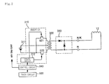
- FIG. 2 shows a configuration of a power supply unit in the background art for supplying the heater voltage shown in FIG. 1 .
- the power supply unit of the background art includes transformer 300, DC voltage source 311, inverter 310 for converting the DC voltage output from DC voltage source 311 into an AC voltage to be supplied to the primary coil of transformer 300, rectifying circuit 330 for rectifying the AC voltage output from the secondary coil of transformer 300 to supply a DC voltage to heater 12, timer circuit 320 to be used for measurement of preheating time, and control circuit 340 that controls the operation of inverter 310 and outputs an HV ON/OFF signal as a control signal for enabling the output of helix voltage Ehel, anode voltage Ea and collector voltage Ecol after a lapse of a predetermined preheating time set up at the time that power is activated based on timer circuit 320.
- Inverter 310 includes transistors Q21 and Q22 for converting the DC voltage output from DC voltage source 311 into an AC voltage and driver circuit 312 for turning on and off transistors Q21 and Q22 alternately.
- Rectifying circuit 330 includes a full-wave rectifying circuit made of two diodes, for example and rectifies the AC voltage output from the secondary coil of transformer 300 to output as heater voltage H a negative DC voltage based on the H/K potential of cathode electrode 11 (not shown).
- the preheating time is set at a sufficiently large value so that the temperature of cathode electrode 11, not illustrated, rises high enough and traveling-wave tube 1 operates stably. For this reason, the preheating time tends to be longer than needed, hence it takes a long time from the activation of the power supply until operation of traveling-wave tube 1 starts.
- heater voltage H is set higher than normal voltage at the time of power activation and then heater voltage H is changed to normal voltage when a temperature sensor detects that cathode electrode 11 has reached a predetermined temperature.
- the timing for sending out an HV ON/OFF signal is also controlled by the control circuit.
- the power supply unit of the background art usually adopts either the method of sending out an HV ON/OFF signal after a lapse of the predetermined preheating time in the same manner as is done at the time of power activation or one of the methods of changing the preheating time in accordance with the time (power failure time) at which the power has been cut off.
- the method of changing the preheating time in accordance with the power failure time it is typical to set the preheating time to be equal to the time of power failure. In this case, however, the maximum of the preheating time is as long as about 3 to 5 minutes, which is the preheating time at the time of power activation.
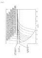
- an effective way is to make the length of the power failure longer than a certain period (longer than 25 seconds in the example shown in FIG. 3 ) as shown in the graph of FIG. 3 , for example.
- a certain period longer than 25 seconds in the example shown in FIG. 3
- the period of power failure is short (instantaneous)
- This problem is attributed to the fact that since there are the parts that support the cathode electrode and the parts that are arranged close to the cathode electrode, it takes time for the cathode electrode and these parts to reach a state of thermal equilibrium.
- FIG. 3 shows how the temperature of the cathode electrode behaves when all the power supply voltages of the traveling-wave tube are turned OFF from normal operation and the state afterwards in which the fixed voltage for normal operation has been applied to the heater for a period of time which is as long as the time in which the power supply voltages have been in an OFF condition. Further, in FIG.
- the present invention at the time that the power supply units are restored to operational status, a voltage higher than that in the normal operation mode of an electron tube is supplied to the heater.
- This configuration makes it possible to raise the temperature of the cathode electrode faster than the background technique. That is, it is possible to make the temperature of the cathode electrode reach the operable temperature of the traveling-wave tube even when the duration of the power failure is short and the duration of the preheating time is set equal the duration of the power failure. As a result, it is possible to shorten the preheating time at the time of restoration from a power failure and make the traveling-wave tube's operation stable after restoration.
- the present invention it is determined at the time of power activation whether the rate of change of the current in the heater is equal to or lower than a predetermined threshold.
- This configuration makes it possible to determine whether the heater reaches the designated temperature. It is thus possible to shorten the preheating time at the time of power activation compared to the background art when a control signal for starting the operation of the electron tube is output at the stage when the heater has reached the designated temperature.
- the target to be supplied with a heater voltage from the power supply unit of the present invention should not be limited to traveling-wave tubes, but any other electron tubes such as klystrons, cathode-ray tubes and the like may be the target as long as they include a heater for supplying thermal energy for emitting electrons from a cathode electrode and starts its operation after preheating the heater is completed.
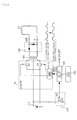
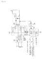
- FIG. 1 is a circuit diagram showing a configuration of the first exemplary embodiment of a power supply unit of the present invention.
- FIG. 5A is a waveform chart showing a voltage waveform and a current waveform in the power supply unit shown in FIG. 4 in normal operation mode after power is activated and
- FIG. 5B is a waveform chart showing a waveform and a current waveform in the power supply unit shown in FIG. 4 during restoration to operational status from a power failure.
- the power supply unit shown in FIG. 4 only includes a configuration of a heater power supply circuit for generating heater voltage H, but the power supply unit may include high-voltage power supply circuits for generating helix voltage Ehel, anode voltage Ea and collector voltage Ecol.
- Heater voltage H and heater current I shown in FIGS. 5A and 5B are shown by schematically illustrating how the voltage and current behave without specifying exact measurements.
- the power supply unit of the first exemplary embodiment includes transformer 100, DC voltage source 111, inverter 110 for converting a DC voltage output from DC voltage source 111 into an AC voltage to be supplied to the primary coil of transformer 100, timer circuit 120, rectifying circuit 130 for rectifying the AC voltage output from the secondary coil of transformer 100 and supplying it to heater 12, control circuit 140 that controls the operation of inverter 110 and outputs an HV ON/OFF signal as a control signal for enabling the output of helix voltage Ehel, anode voltage Ea and collector voltage Ecol output, and power failure detecting circuit 150 for detecting a power failure.
- Inverter 110 includes transistors Q1 and Q2 for converting the DC voltage output from DC voltage source 111 into an AC voltage and driver circuit 112 for alternately turning on and off transistors Q1 and Q2.
- Power failure detecting circuit 150 includes comparator 151, and compares the output voltage from DC voltage source 111 with predetermined threshold voltage Vth and outputs the result of the comparison to control circuit 140 to thereby give a notice of either detection or non-detection of a power failure.
- Rectifying circuit 130 includes a full-wave rectifying circuit made of two diodes, for example, and rectifies the AC voltage output from the secondary coil of transformer 100 to output as heater voltage H a negative DC voltage based on the H/K potential of cathode electrode 11.
- Control circuit 140 can be embodied by an LSI including logical circuits and memory or a processor (computer) including a CPU and a recording medium having a program for realizing the process to be executed by the CPU.
- a processor computer
- the function of control circuit 140 described hereinbelow can be realized by a CPU that executes the process in accordance with the program stored in the recording medium.
- FIG. 4 shows a configuration in which timer circuit 120 is provided independently, the timer circuit is not needed if control circuit 140 has a timer function.
- heater voltage H is boosted using a predetermined time constant, and then is controlled to be kept at a predetermined fixed level (normal voltage) as shown in FIG. 5A . Since heater 12 has a characteristic in which its resistance becomes greater as the temperature increases, current I passing through heater 12 takes a maximum value immediately after the power is activated, and then current I gradually decreases as the resistance increases.
- heater voltage H when the power supply is restored after a power failure, heater voltage H is set at a level higher than the normal voltage and then is changed to the fixed level or the normal voltage as shown in FIG. 5B .
- heater voltage H immediately after restoration of the power supply after a power failure is set so that the maximum value of heater current I is equal to or lower than a predetermined current limit level, taking into account the stress on heater 12 and cathode electrode 11.
- Supplying voltage H, at a voltage that is higher than the normal voltage, to heater 12 at the time that the power supply is restored after power failure in the above way enables the temperature of cathode electrode 11 to rise faster than that in the case of the background art.
- cathode electrode 11 reach the operable temperature even if the duration of power failure is short, and the duration of the preheating time is set to equal the duration of power failure.
- Heater voltage H can be controlled by switching the pulse width of the driving signal to be supplied from control circuit 140 to driver circuit 112 as shown in FIG. 4 .
- a first driving signal having a relatively narrow pulse width is supplied to transistors Q1 and Q2 from control circuit 140 by way of drive circuit 112.
- a second driving signal having a pulse width wider than that of the normal operation is supplied to transistors Q1 and Q2 from control circuit 140 by way of drive circuit 112.
- heater voltage H takes a value proportional to the pulse width while transistors Q1 and Q2 are on. That is, heater voltage H driven by the second driving signal is higher than heater voltage H driven by the first driving signal.
- heater voltage H may be controlled by providing regulator circuit 160 between DC voltage source 111 and the primary coil of transformer 100 and by supplying a regulator driving signal from control circuit 140 to regulator circuit 160, as shown in FIG. 6 .
- Regulator circuit 160 shown in FIG. 6 is a boost type circuit for boosting the DC voltage output from DC voltage source 111, and includes inductance L1 and diode D1 which are connected in series between the output terminal of DC voltage source 111 and the center tap of the primary coil of transformer 100 and includes a transistor Q3 connected in parallel with DC voltage source 111.
- regulator circuit 160 shown in FIG. 6 energy is accumulated in inductance L1 while transistor Q3 is on, whereas the energy accumulated in inductance L1 is supplied to inverter 110 via diode D1 while transistor Q3 is off.
- the boosted voltage can be controlled by the pulse width of the driving signal supplied to the base of transistor Q3, hence it is possible to supply a boosted voltage proportional to the pulse width to inverter 110.
- regulator circuit 160 shown in FIG. 6 When regulator circuit 160 shown in FIG. 6 is arranged between DC voltage source 111 and the primary coil of transformer 100, during normal operation the first driving signal having a relatively narrow pulse width is supplied from control circuit 140 to transistor Q3 of regulator circuit 160. On the other hand, at the time that the power supply is restored after a power failure (instantaneous cutoff), the second driving signal having a pulse width wider than that in the normal operation mode is supplied from control circuit 140 to transistor Q3 of regulator circuit 160. In this case, heater voltage H takes a value proportional to the pulse width while transistor Q3 is on. That is, heater voltage H driven by the second driving signal is higher than heater voltage H driven by the first driving signal.
- a driving signal having a fixed pulse width may and should be supplied to inverter 110.
- the driving signal supplied to regulator circuit 160 and the driving signal supplied to inverter 110 may or may not be synchronized with each other.
- the driving signal supplied to regulator circuit 160 is synchronized with the driving signal supplied to inverter 110, the frequency components of the driving signal leaking toward the secondary coil of transformer 100 decrease, so that noise components contained in heater voltage H can be reduced.
- regulator circuit 160 a well-known buck-boost type circuit may also be used to perform control instead of the boost type circuit shown in FIG. 6 .
- buck-boost type circuit in the normal operation mode, a driving signal having a relatively wide pulse width is supplied from control circuit 140 to regulator circuit 160, at the time that the power supply is restored after a power failure (instantaneous cutoff) a driving signal having a pulse width narrower than that in the normal operation mode is supplied from control circuit 140 to regulator circuit 160, whereby it is possible to set heater voltage H to be higher than the normal voltage.
- Regulator circuit 160 may be used any type of well-known circuits if the pulse width of the driving signal supplied from control circuit 140 is set up appropriately in accordance with the input/output characteristics.
- FIG. 7 is a flow chart showing the operation for restoration of the power supply units shown in FIG. 4 and 6 .
- control circuit 140 observes the output signal from power failure detecting circuit 150 and checks whether the output signal from power failure detecting circuit 150 detects a power failure (Step S1). When the output signal from power failure detecting circuit 150 shows no detection of a power failure, the operation returns to Step S1 to continue observation of the output signal from power failure detecting circuit 150.
- control circuit 140 stops outputting the first driving signal to driver circuit 112 to stop the output of heater voltage H. Also, control circuit 140 stops outputting an HV ON/OFF signal to stop the output of helix voltage Ehel, anode voltage Ea and collector voltage Ecol from a high-voltage power supply circuit, not illustrated, (Step S2). At the same time control circuit 140 causes timer circuit 120 to measure the duration of the power failure.
- Control circuit 140 again observes the output signal from power failure detecting circuit 150 to check whether the output signal from power failure detecting circuit 150 shows detection of a power failure (whether the normal state has been restored from the power failure) (Step S3).
- the output signal from power failure detecting circuit 150 shows detection of a power failure (during power failure)
- the operation returns to Step S3 and continues observation of the output signal from power failure detecting circuit 150.
- control circuit 140 When the output signal from power failure detecting circuit 150 shows no detection of a power failure (restoration from the power failure), control circuit 140 outputs the second driving signal to driver circuit 112 to let it output heater voltage H that is higher than the normal voltage if the power supply circuit has the configuration shown in FIG. 4 .
- control circuit 140 when control circuit 140 has the configuration shown in FIG. 6 , control circuit 140 outputs the second driving signal to transistor Q3 of regulator circuit 160 to let it output heater voltage H that is higher than the normal voltage (Step S4).
- the output period of the second driving signal may coincide with the duration of the power failure that was measured by timer circuit 120.
- control circuit 140 when the power supply circuit has the configuration shown in FIG. 4 , outputs the first driving signal to driver circuit 112 to let it output the normal voltage and also outputs an HV ON/OFF signal so as to cause a high-voltage power supply circuit, not illustrated, to output helix voltage Ehel, anode voltage Ea and collector voltage Ecol to restart the operation of traveling-wave tube 1.
- the power supply circuit has the configuration shown in FIG. 4
- control circuit 140 outputs the first driving signal to transistor Q3 of regulator circuit 160 so as to output the normal voltage and also outputs an HV ON/OFF signal so as to cause a high-voltage power supply circuit, not illustrated, to output helix voltage Ehel, anode voltage Ea and collector voltage Ecol to restart the operation of traveling-wave tube 1 (Step S5).
- the power supply unit of the present exemplary embodiment if a power failure of DC voltage source 11 occurs in the normal operation mode of traveling-wave tube 1, it is possible to raise the temperature of cathode electrode 11 of traveling-wave tube 1 faster than the background art does by supplying a voltage higher than the normal voltage to heater 12 at the time that the power supply is restored after a power failure.
- cathode electrode 11 reach the operable temperature of traveling-wave tube 1 in a shorter time.
- preheating time is set equal to the power failure time and the power failure time is short, then preheating time is short, and it is possible to make cathode electrode 11 reach the operable temperature of traveling-wave tube 1.
- the power supply unit of the exemplary embodiment is effectively applied to an event of a so called instantaneous power failure in which the duration of the power failure is short and in which the temperature of cathode electrode 11 is high compared with the state in which cathode electrode 11 is totally cooled condition when, for example, the power supply unit is activated.
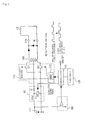
- FIG. 8 is a circuit diagram showing a configuration of the second exemplary embodiment of a power supply unit of the present invention.
- FIG. 9 is a waveform chart showing a voltage waveform and current waveform output from the heater power supply circuit shown in FIG. 8 .
- the power supply unit shown in FIG. 8 only includes a configuration of a heater power supply circuit for generating heater voltage H, but the power supply unit may include high-voltage power supply circuits for generating helix voltage Ehel, anode voltage Ea and collector voltage Ecol.
- Heater voltage H and heater current I shown in FIG. 9 are shown by schematically illustrating how the voltage and current behave without specifying exact measurements.
- the power supply unit of the second exemplary embodiment includes transformer 200, DC voltage source 211, inverter 210 for converting the DC voltage output from DC voltage source 211 into an AC voltage to be supplied to the primary coil of transformer 200, timer circuit 220, rectifying circuit 230 for rectifying the AC voltage output from the secondary coil of transformer 200 and supplying it to heater 12, control circuit 240 that controls the operation of inverter 210 and outputs an HV ON/OFF signal as a control signal for enabling the output of helix voltage Ehel, anode voltage Ea and collector voltage Ecol, current detector 250 for detecting the current (heater current I) flowing through heater 12 and A/D converter 270 for A/D converting heater current I detected by current detector 250 and supplying the result to control circuit 240.
- Inverter 210 includes transistors Q11 and Q12 for converting the DC voltage output from DC voltage source 211 into an AC voltage and driver circuit 212 for alternately turning on and off transistors Q11 and Q12.
- Rectifying circuit 230 includes a full-wave rectifying circuit made of two diodes, for example and rectifies the AC voltage output from the secondary coil of transformer 200 to output as heater voltage H a negative DC voltage based on the H/K potential of cathode electrode 11.
- Current detector 250 is connected to secondary transformer 200 to detect the current flowing through heater 12. The measurement detected by current detector 250 is converted into a digital signal by A/D converter 270 to be supplied to control circuit 240.
- Control circuit 240 can be embodied by an LSI including logical circuits and memory or a processor (computer) including a CPU and a recording medium having a program for realizing the process to be executed by the CPU.
- a processor computer
- the function of control circuit 240 described hereinbelow can be realized by a CPU that executes the process in accordance with the program stored in the recording medium.
- FIG. 8 shows a configuration in which timer circuit 220 is provided independently, the timer circuit is not needed if control circuit 240 has a timer function. Also, FIG. 8 shows a configurational example in which the output signal from current detector 250 is converted by using A/D converter 270 into a digital signal, which is supplied to control circuit 240. However, if control circuit 240 can directly process the output signal (analog signal) from current detector 250, A/D converter 270 is not needed.
- the heater voltage is boosted using a predetermined time constant and then is controlled to be kept at a predetermined fixed level (normal voltage) as shown in FIG. 9 . Since heater 12 has a characteristic in which its resistance becomes greater as the temperature increases, the current passing through heater 12 takes a maximum value immediately after power activation, and then the current gradually decreases as the resistance increases.
- the rate of change (Dl) of heater current I detected by current detector 250 is calculated for every predetermined unit time (Dt) by the process of control circuit 240 so that the control circuit determines that heater 12 has reached the designated temperature when the rate of change becomes equal to or lower than a predetermined threshold and outputs HV ON/OFF signal.
- the heater voltage H that is set higher than the normal voltage and its application time should be set appropriately so that the stress given to the heater or the cathode electrode will not shorten the life of the heater or degrade the performance of the cathode electrode.
- the power supply unit of the second exemplary embodiment it is determined whether heater 12 reaches the designated temperature by detecting the rate of change of the current flowing through heater 12. Accordingly, it is possible to start the operation of traveling-wave tube 1 by outputting an HV ON/OFF signal when the rate of change of the current flowing through the heater falls within the predetermined threshold range, without the need to wait for a lapse of the predetermined preheating time using a timer circuit as in the power supply unit of the background art.
- heater voltage H is slightly increased to let current I flowing through heater 12 be greater for a predetermined fixed period when the rate of change of heater current I falls within the predetermined threshold range. In this way it is possible to shorten the time for cathode electrode 11 to reach a state of thermal equilibrium by excessively heating cathode electrode 11, so that traveling-wave tube 1 can operate stably if helix voltage Ehel, anode voltage Ea and collector voltage Ecol are supplied.
- traveling-wave tube 1 When traveling-wave tube 1 is small, and when there are a few parts arranged near the cathode electrode and in other cases where cathode electrode 11 is assumed to have fully reached a state of thermal equilibrium when the rate of change of the current flowing through the heater falls within the predetermined threshold range, operation of traveling-wave tube 1 may be started by outputting an HV ON/OFF signal from control circuit 240 without performing excessive heating.
- Heater voltage H can be controlled by switching the pulse width of the driving signal to be supplied from control circuit 240 to driver circuit 212 as shown in FIG. 8 . Specifically, at the time that power is activated, a first driving signal having a relatively narrow pulse width is supplied to transistors Q11 and Q12 from control circuit 240 by way of drive circuit 212. When cathode electrode 11 is heated to excess, a second driving signal having a pulse width wider than that of the normal operation is supplied to transistors Q11 and Q12 from control circuit 240 by way of drive circuit 212. In this case, heater voltage H takes a value proportional to the pulse width while transistors Q11 and Q12 are on. That is, heater voltage H driven by the second driving signal is higher than heater voltage H driven by the first driving signal.
- heater voltage H may be controlled by providing regulator circuit 260 between DC voltage source 211 and the primary coil of transformer 200 and by supplying a regulator driving signal from control circuit 240 to regulator circuit 260, as shown in FIG. 10 .
- Regulator circuit 260 shown in FIG. 10 is a boost type circuit for boosting the DC voltage output from DC voltage source 211, and includes inductance L11 and diode D11 which are connected in series between the output terminal of DC voltage source 211 and the center tap of the primary coil of transformer 200 and includes a transistor Q13 connected in parallel with DC voltage source 211.
- regulator circuit 260 shown in FIG. 10 energy is accumulated in inductance L11 while transistor Q13 is on, whereas the energy accumulated in inductance L11 is supplied to inverter 210 via diode D11 while transistor Q13 is off.
- the boosted voltage can be controlled by the pulse width of the driving signal supplied to the base of transistor Q13, hence it is possible to supply a boosted voltage proportional to the pulse width to inverter 210.
- regulator circuit 260 shown in FIG. 10 When regulator circuit 260 shown in FIG. 10 is arranged between DC voltage source 211 and the primary coil of transformer 200, at the time that power is activated the first driving signal having a relatively narrow pulse width is supplied from control circuit 240 to transistor Q13 of regulator circuit 260. On the other hand, at the time of excessively heating cathode electrode 11, the second driving signal having a pulse width wider than that in the normal operation mode is supplied from control circuit 240 to transistor Q13 of regulator circuit 260. In this case, heater voltage H takes a value proportional to the pulse width while transistor Q13 is on. That is, heater voltage H driven by the second driving signal is higher than heater voltage H driven by the first driving signal.
- a driving signal having a fixed pulse width may and should be supplied to inverter 210.
- the driving signal supplied to regulator circuit 260 and the driving signal supplied to inverter 210 may or may not be synchronized with each other.
- the driving signal supplied to regulator circuit 260 is synchronized with the driving signal supplied to inverter 210, the frequency components of the driving signal leaking toward the secondary coil of transformer 200 decrease, so that noise components contained in heater voltage H can be reduced.
- regulator circuit 260 a well-known buck-boost type circuit may also be used to perform control instead of the boost type circuit shown in FIG. 10 .
- a driving signal having a relatively wide pulse width is supplied from control circuit 240 to regulator circuit 260, whereas while cathode electrode 11 is heated excessively, a driving signal having a pulse width narrower than that at the normal operation is supplied from control circuit 240 to regulator circuit 260, whereby it is possible to set heater voltage H to be higher than the normal voltage.
- Regulator circuit 260 may be used any type of well-known circuits if the pulse width of the driving signal supplied from control circuit 240 is set up appropriately in accordance with the input/output characteristics.
- FIG. 11 is a flow chart showing the operation of the power supply units shown in FIGS. 8 and 10 at the time that power is activated.
- control circuit 240 outputs the first driving signal to driver circuit 212 at the time that power is activated to let it output the heater voltage. Also, the control circuit observes the current detected value supplied from A/D converter 270 and calculates the rate of change of heater current I per predetermined unit time (Step S11).
- control circuit 240 compares the calculated rate of change of heater current I with a predetermined threshold, and determines whether the rate of change of heater current I is equal to or smaller than the threshold (Step S12). When the rate of change of heater current I is greater than the threshold, the operation returns to Step S1, to continue calculation of the rate of change of heater current 1.
- control circuit 240 When the rate of change of heater current I is equal to or lower than the threshold, control circuit 240 outputs the second driving signal to driver circuit 212 to let it output heater voltage H that is higher than the normal voltage if the power supply circuit has the configuration shown in FIG. 8 .
- control circuit 240 has the configuration shown in FIG. 10 , the control circuit outputs the second driving signal to transistor Q13 of regulator circuit 260 to let it output heater voltage H that is higher than the normal voltage (Step S18), In this process, control circuit 240 outputs the second driving signal to driver circuit 212 for a predetermined fixed period, using timer circuit 220.
- control circuit 240 when the power supply circuit has the configuration shown in FIG. 8 , outputs the first driving signal to driver circuit 212 to let it output the normal voltage and also outputs an HV ON/OFF signal so as to cause a high-voltage power supply circuit, not illustrated, to output helix voltage Ehel, anode voltage Ea and collector voltage Ecol to start the operation of traveling-wave tube 1.
- the power supply circuit has the configuration shown in FIG. 8
- control circuit 240 outputs the first driving signal to transistor Q13 of regulator circuit 260 so as to output the normal voltage and also outputs an HV ON/OFF signal so as to cause a high-voltage power supply circuit, not illustrated, to output helix voltage Ehel, anode voltage Ea and collector voltage Ecol to restart the operation of traveling-wave tube 1 (Step S14).
- the control signal for starting the operation of traveling-wave tube 1 is output at this stage, so that it is possible to shorten the preheating time at the time that power is activated compared to the background art. Further, when a voltage higher than the normal voltage is supplied at the moment that the rate of change of heater current I becomes equal to or lower than the threshold so as to excessively heat cathode electrode 11, the transfer of cathode electrode 1 to the state of thermal equilibrium can be promoted. Accordingly, it is possible to make traveling-wave tube 1 operate in a stable manner.
- the power supply unit of the second exemplary embodiment since the current flowing through the secondary coil of transformer 200 is detected by current detector 250, it is hence possible to detect the occurrence of a power failure at DC voltage source 211 and restoration of the power supply after a power failure based on th presence of the current.
- the power supply unit of the second exemplary embodiment can also execute the same process as in the first exemplary embodiment at the time of restoration of the power supply after a power failur by rewriting the program of control circuit 240.
- control circuit 240 is adapted to observe the current flowing through the secondary coil of transformer 200 by use of current detector 250.
- the control circuit determines that no power failure is occurring, returns to the process at Step S1 shown in FIG. 7 and continues observation of the presence of the current by current detector 250.
- the control circuit determines that a power failure has occurred.
- control circuit stops outputting the first driving signal to driver circuit 212 so as to stop output of heater voltage H and stops outputting an HV ON/OFF signal so as to stop output of helix voltage Ehel, anode voltage Ea and collector voltage Ecol. Then in the process at Step S3 shown in FIG.
- the control circuit causes heater voltage H that is higher than that in the normal operation to output at Step S4 in the same manner as in the first exemplary embodiment, and then causes heater voltage H in the normal operation mode to output after a lapse of the predetermined period at Step S5 while outputting an HV ON/OFF signal so as to supply helix voltage Ehel, anode voltage Ea and collector voltage Eco to traveling-wave tube 1.
- the power supply unit of the second exemplary embodiment shown in FIG. 8 or FIG. 10 may be provided with power failure detecting circuit 150 so that power failure detecting circuit 150 may detect a power failure that occurs in DC voltage source 211 and restoration of the power supply after a power failure, in the same manner as in the first exemplary embodiment.
- Execution of this process makes it possible to shorten the preheating time of the heater provided for traveling-wave tube 1, both at the time of power activation and at the time of restoration of the power supply after a power failure.
- the power supply unit of the second exemplary embodiment may be constructed so as to output heater voltage H that is higher than that in the normal operation mode at the time of restoration of the power supply after a power failure in the same manner as in the first exemplary embodiment while calculating the rate of change of heater current I flowing through the secondary coil of transformer 200 similarly to the time of power activation.
- the rate of change of heater current I falls equal to or lower than the predetermined threshold, the operation of traveling-wave tube 1 may be started by returning heater voltage H to the normal voltage and outputting an HV ON/OFF signal.
- the power supply unit of the present exemplary embodiment is not only used to supply various power supply voltages to an electron tube whose thermal structure around the cathode electrode is known but is also used to supply various power voltages to a variety of electron tubes whose thermal structure around the cathode electrode is unknown as long as the power supply unit is used within the rated capacity. That is, the power supply unit is highly versatile.
Landscapes
- Microwave Tubes (AREA)
- Circuit Arrangements For Discharge Lamps (AREA)
Priority Applications (1)
| Application Number | Priority Date | Filing Date | Title |
|---|---|---|---|
| EP15194725.6A EP3021346B1 (fr) | 2007-03-19 | 2008-03-18 | Système de circuit haute fréquence et procédé de contrôle de la tension d'un chauffage |
Applications Claiming Priority (1)
| Application Number | Priority Date | Filing Date | Title |
|---|---|---|---|
| JP2007070519A JP5114079B2 (ja) | 2007-03-19 | 2007-03-19 | 電源装置、高周波回路システム及びヒータ電圧制御方法 |
Related Child Applications (1)
| Application Number | Title | Priority Date | Filing Date |
|---|---|---|---|
| EP15194725.6A Division EP3021346B1 (fr) | 2007-03-19 | 2008-03-18 | Système de circuit haute fréquence et procédé de contrôle de la tension d'un chauffage |
Publications (2)
| Publication Number | Publication Date |
|---|---|
| EP1973138A2 true EP1973138A2 (fr) | 2008-09-24 |
| EP1973138A3 EP1973138A3 (fr) | 2015-08-12 |
Family
ID=39587919
Family Applications (2)
| Application Number | Title | Priority Date | Filing Date |
|---|---|---|---|
| EP08152876.2A Withdrawn EP1973138A3 (fr) | 2007-03-19 | 2008-03-18 | Unité d'alimentation électrique, système de circuit haute fréquence et procédé de contrôle de la tension d'un chauffage |
| EP15194725.6A Active EP3021346B1 (fr) | 2007-03-19 | 2008-03-18 | Système de circuit haute fréquence et procédé de contrôle de la tension d'un chauffage |
Family Applications After (1)
| Application Number | Title | Priority Date | Filing Date |
|---|---|---|---|
| EP15194725.6A Active EP3021346B1 (fr) | 2007-03-19 | 2008-03-18 | Système de circuit haute fréquence et procédé de contrôle de la tension d'un chauffage |
Country Status (3)
| Country | Link |
|---|---|
| US (1) | US7800311B2 (fr) |
| EP (2) | EP1973138A3 (fr) |
| JP (1) | JP5114079B2 (fr) |
Families Citing this family (9)
| Publication number | Priority date | Publication date | Assignee | Title |
|---|---|---|---|---|
| KR101334206B1 (ko) * | 2007-06-27 | 2013-11-29 | 삼성전자주식회사 | 화상독취장치 및 그 방법 |
| JP5136901B2 (ja) * | 2008-10-09 | 2013-02-06 | 株式会社ネットコムセック | 温度検出装置 |
| JP5311464B2 (ja) | 2008-11-25 | 2013-10-09 | 株式会社ネットコムセック | 電流測定回路 |
| EP3137808B1 (fr) | 2014-04-29 | 2018-02-28 | Philips Lighting Holding B.V. | Système d'éclairage d'urgence et procédé pour égalisation automatique de puissance de chauffage. |
| JP6760949B2 (ja) * | 2015-09-24 | 2020-09-23 | Necネットワーク・センサ株式会社 | 電子銃、電子管及び高周波回路システム |
| KR102448410B1 (ko) * | 2018-11-28 | 2022-09-28 | 주식회사 레메디 | 추출기를 가지는 소형 엑스레이 튜브 |
| WO2021007463A1 (fr) * | 2019-07-09 | 2021-01-14 | Varex Imaging Corporation | Pilote de canon à électrons |
| BR112022013243A2 (pt) * | 2020-01-23 | 2022-09-06 | Arris Entpr Llc | Sistema e método para detecção aprimorada de interrupção da energia fornecida por uma rede elétrica ca a um dispositivo |
| US12100570B2 (en) | 2020-05-28 | 2024-09-24 | Nec Network And Sensor Systems, Ltd. | Power supply device, microwave tube device, power supply method, and recording medium |
Citations (2)
| Publication number | Priority date | Publication date | Assignee | Title |
|---|---|---|---|---|
| JPH06310045A (ja) | 1993-04-27 | 1994-11-04 | Mitsubishi Electric Corp | 進行波管ヒータ電源 |
| JP2007070519A (ja) | 2005-09-08 | 2007-03-22 | Yokohama Rubber Co Ltd:The | シーリング材組成物 |
Family Cites Families (11)
| Publication number | Priority date | Publication date | Assignee | Title |
|---|---|---|---|---|
| US4894587A (en) * | 1984-08-17 | 1990-01-16 | Lutron Electronics Co., Inc. | High frequency gas discharge lamp dimming ballast |
| JPS6364298A (ja) * | 1986-09-05 | 1988-03-22 | Hitachi Medical Corp | 自動輝度調整機構付x線装置 |
| GB2227133A (en) * | 1989-01-14 | 1990-07-18 | Ferranti Int Signal | Control of power inverter |
| JPH04324298A (ja) * | 1991-04-24 | 1992-11-13 | Toshiba Corp | X線発生装置 |
| US5449979A (en) * | 1992-09-25 | 1995-09-12 | Matsushita Electric Works, Ltd. | Inverter power supply |
| US5500621A (en) * | 1995-04-03 | 1996-03-19 | Martin Marietta Corp. | Travelling-wave tube protection arrangement |
| JP2002093595A (ja) * | 2000-09-14 | 2002-03-29 | Toshiba Corp | X線高電圧装置 |
| US6753651B1 (en) * | 2002-05-01 | 2004-06-22 | The Bodine Company, Inc. | Emergency ballast with battery heater |
| JP2004007161A (ja) * | 2002-05-31 | 2004-01-08 | Matsushita Electric Ind Co Ltd | マイクロ波発振機 |
| JP2005116355A (ja) * | 2003-10-08 | 2005-04-28 | Nec Microwave Inc | マイクロ波管システム及びマイクロ波管 |
| US7589480B2 (en) * | 2006-05-26 | 2009-09-15 | Greenwood Soar Ip Ltd. | High intensity discharge lamp ballast |
-
2007
- 2007-03-19 JP JP2007070519A patent/JP5114079B2/ja active Active
-
2008
- 2008-03-18 US US12/050,609 patent/US7800311B2/en active Active
- 2008-03-18 EP EP08152876.2A patent/EP1973138A3/fr not_active Withdrawn
- 2008-03-18 EP EP15194725.6A patent/EP3021346B1/fr active Active
Patent Citations (2)
| Publication number | Priority date | Publication date | Assignee | Title |
|---|---|---|---|---|
| JPH06310045A (ja) | 1993-04-27 | 1994-11-04 | Mitsubishi Electric Corp | 進行波管ヒータ電源 |
| JP2007070519A (ja) | 2005-09-08 | 2007-03-22 | Yokohama Rubber Co Ltd:The | シーリング材組成物 |
Also Published As
| Publication number | Publication date |
|---|---|
| EP1973138A3 (fr) | 2015-08-12 |
| US7800311B2 (en) | 2010-09-21 |
| EP3021346A1 (fr) | 2016-05-18 |
| US20080231197A1 (en) | 2008-09-25 |
| JP2008234907A (ja) | 2008-10-02 |
| EP3021346B1 (fr) | 2021-07-07 |
| JP5114079B2 (ja) | 2013-01-09 |
Similar Documents
| Publication | Publication Date | Title |
|---|---|---|
| EP3021346B1 (fr) | Système de circuit haute fréquence et procédé de contrôle de la tension d'un chauffage | |
| JP5513829B2 (ja) | 電流駆動回路 | |
| JP5348028B2 (ja) | チョッパ回路の故障検出装置 | |
| US7764025B2 (en) | Power supply apparatus and high-frequency circuit system | |
| US20070164689A1 (en) | Lighting circuit | |
| EP1814134A2 (fr) | Appareil d'alimentation électrique et système de circuit haute fréquence | |
| US10973112B2 (en) | Charged particle beam device | |
| JP5136892B2 (ja) | 電圧制御装置、電源装置、電子管及び高周波回路システム | |
| CN109962511B (zh) | 半导体装置 | |
| US7898346B2 (en) | Power supply apparatus and high-frequency circuit system | |
| CN114583929B (zh) | Dc电源的过流保护电路和过流保护方法 | |
| US8937979B2 (en) | Gas laser oscillator having function to determine initiation of electric discharge | |
| US7315134B2 (en) | Power supply for a high voltage device | |
| JP2017069561A (ja) | ガスレーザ発振装置 | |
| CN114070280B (zh) | 一种三极管驱动控制电路、方法和驱动系统 | |
| KR102954550B1 (ko) | 진행파관 증폭기의 예열 모드에 따른 히터 전류 제한 회로 및 그 제어 방법 | |
| CN120064352A (zh) | 荧光x射线分析装置和电源装置 | |
| JP5656270B1 (ja) | 電源装置、高周波システム及び該電源装置の制御方法 | |
| JP4363310B2 (ja) | マグネトロン駆動用電源 | |
| JPS63318091A (ja) | 高周波加熱装置 | |
| JPH1154817A (ja) | マイクロ波励起ガスレーザ発振装置 | |
| JP2020054100A (ja) | スイッチング電源装置 | |
| JP2016158465A (ja) | 電源装置 | |
| JP2003036990A (ja) | 点灯装置、高圧放電灯を備えた点灯装置 |
Legal Events
| Date | Code | Title | Description |
|---|---|---|---|
| PUAI | Public reference made under article 153(3) epc to a published international application that has entered the european phase |
Free format text: ORIGINAL CODE: 0009012 |
|
| AK | Designated contracting states |
Kind code of ref document: A2 Designated state(s): AT BE BG CH CY CZ DE DK EE ES FI FR GB GR HR HU IE IS IT LI LT LU LV MC MT NL NO PL PT RO SE SI SK TR |
|
| AX | Request for extension of the european patent |
Extension state: AL BA MK RS |
|
| RAP1 | Party data changed (applicant data changed or rights of an application transferred) |
Owner name: NETCOMSEC CO., LTD |
|
| RIC1 | Information provided on ipc code assigned before grant |
Ipc: H01J 19/16 20060101AFI20150318BHEP |
|
| PUAL | Search report despatched |
Free format text: ORIGINAL CODE: 0009013 |
|
| AK | Designated contracting states |
Kind code of ref document: A3 Designated state(s): AT BE BG CH CY CZ DE DK EE ES FI FR GB GR HR HU IE IS IT LI LT LU LV MC MT NL NO PL PT RO SE SI SK TR |
|
| AX | Request for extension of the european patent |
Extension state: AL BA MK RS |
|
| RIC1 | Information provided on ipc code assigned before grant |
Ipc: H01J 19/16 20060101AFI20150707BHEP |
|
| RAP1 | Party data changed (applicant data changed or rights of an application transferred) |
Owner name: NEC NETWORK AND SENSOR SYSTEMS, LTD. |
|
| RAP1 | Party data changed (applicant data changed or rights of an application transferred) |
Owner name: NEC NETWORK AND SENSOR SYSTEMS, LTD. |
|
| AKX | Designation fees paid |
Designated state(s): DE GB |
|
| AXX | Extension fees paid |
Extension state: AL Extension state: MK Extension state: BA Extension state: RS |
|
| STAA | Information on the status of an ep patent application or granted ep patent |
Free format text: STATUS: THE APPLICATION IS DEEMED TO BE WITHDRAWN |
|
| 18D | Application deemed to be withdrawn |
Effective date: 20160213 |