EP1975699A2 - Verfahren und System zur Strukturierung einer Maskenschicht - Google Patents
Verfahren und System zur Strukturierung einer Maskenschicht Download PDFInfo
- Publication number
- EP1975699A2 EP1975699A2 EP20080151996 EP08151996A EP1975699A2 EP 1975699 A2 EP1975699 A2 EP 1975699A2 EP 20080151996 EP20080151996 EP 20080151996 EP 08151996 A EP08151996 A EP 08151996A EP 1975699 A2 EP1975699 A2 EP 1975699A2
- Authority
- EP
- European Patent Office
- Prior art keywords
- pattern
- printed circuit
- soldermask
- layer
- circuit board
- Prior art date
- Legal status (The legal status is an assumption and is not a legal conclusion. Google has not performed a legal analysis and makes no representation as to the accuracy of the status listed.)
- Granted
Links
- 238000000034 method Methods 0.000 title claims abstract description 73
- 238000000059 patterning Methods 0.000 title description 8
- 239000000463 material Substances 0.000 claims description 47
- RYGMFSIKBFXOCR-UHFFFAOYSA-N Copper Chemical compound [Cu] RYGMFSIKBFXOCR-UHFFFAOYSA-N 0.000 description 7
- 229910052802 copper Inorganic materials 0.000 description 7
- 239000010949 copper Substances 0.000 description 7
- 239000000758 substrate Substances 0.000 description 7
- 238000007796 conventional method Methods 0.000 description 5
- CDBYLPFSWZWCQE-UHFFFAOYSA-L Sodium Carbonate Chemical compound [Na+].[Na+].[O-]C([O-])=O CDBYLPFSWZWCQE-UHFFFAOYSA-L 0.000 description 4
- 239000011248 coating agent Substances 0.000 description 2
- 238000000576 coating method Methods 0.000 description 2
- 239000012530 fluid Substances 0.000 description 2
- 229910000029 sodium carbonate Inorganic materials 0.000 description 2
- 230000015572 biosynthetic process Effects 0.000 description 1
- 230000000903 blocking effect Effects 0.000 description 1
- 238000004132 cross linking Methods 0.000 description 1
- 230000000694 effects Effects 0.000 description 1
- 239000004744 fabric Substances 0.000 description 1
- 238000009472 formulation Methods 0.000 description 1
- 239000011521 glass Substances 0.000 description 1
- 238000003384 imaging method Methods 0.000 description 1
- 229910010272 inorganic material Inorganic materials 0.000 description 1
- 239000011147 inorganic material Substances 0.000 description 1
- 238000001459 lithography Methods 0.000 description 1
- 238000004519 manufacturing process Methods 0.000 description 1
- 230000000873 masking effect Effects 0.000 description 1
- 239000000203 mixture Substances 0.000 description 1
- 239000011368 organic material Substances 0.000 description 1
- 230000001151 other effect Effects 0.000 description 1
- 239000012782 phase change material Substances 0.000 description 1
- 229920002120 photoresistant polymer Polymers 0.000 description 1
- 239000004033 plastic Substances 0.000 description 1
- 229920003023 plastic Polymers 0.000 description 1
- BWHMMNNQKKPAPP-UHFFFAOYSA-L potassium carbonate Chemical compound [K+].[K+].[O-]C([O-])=O BWHMMNNQKKPAPP-UHFFFAOYSA-L 0.000 description 1
- 230000005855 radiation Effects 0.000 description 1
- 239000004065 semiconductor Substances 0.000 description 1
- 239000002195 soluble material Substances 0.000 description 1
- 238000005507 spraying Methods 0.000 description 1
- 238000003860 storage Methods 0.000 description 1
- 239000000126 substance Substances 0.000 description 1
- 239000000725 suspension Substances 0.000 description 1
- XLYOFNOQVPJJNP-UHFFFAOYSA-N water Substances O XLYOFNOQVPJJNP-UHFFFAOYSA-N 0.000 description 1
Images





Classifications
-
- G—PHYSICS
- G03—PHOTOGRAPHY; CINEMATOGRAPHY; ANALOGOUS TECHNIQUES USING WAVES OTHER THAN OPTICAL WAVES; ELECTROGRAPHY; HOLOGRAPHY
- G03F—PHOTOMECHANICAL PRODUCTION OF TEXTURED OR PATTERNED SURFACES, e.g. FOR PRINTING, FOR PROCESSING OF SEMICONDUCTOR DEVICES; MATERIALS THEREFOR; ORIGINALS THEREFOR; APPARATUS SPECIALLY ADAPTED THEREFOR
- G03F7/00—Photomechanical, e.g. photolithographic, production of textured or patterned surfaces, e.g. printing surfaces; Materials therefor, e.g. comprising photoresists; Apparatus specially adapted therefor
- G03F7/20—Exposure; Apparatus therefor
- G03F7/2002—Exposure; Apparatus therefor with visible light or UV light, through an original having an opaque pattern on a transparent support, e.g. film printing, projection printing; by reflection of visible or UV light from an original such as a printed image
- G03F7/2014—Contact or film exposure of light sensitive plates such as lithographic plates or circuit boards, e.g. in a vacuum frame
- G03F7/2016—Contact mask being integral part of the photosensitive element and subject to destructive removal during post-exposure processing
- G03F7/2018—Masking pattern obtained by selective application of an ink or a toner, e.g. ink jet printing
-
- H—ELECTRICITY
- H05—ELECTRIC TECHNIQUES NOT OTHERWISE PROVIDED FOR
- H05K—PRINTED CIRCUITS; CASINGS OR CONSTRUCTIONAL DETAILS OF ELECTRIC APPARATUS; MANUFACTURE OF ASSEMBLAGES OF ELECTRICAL COMPONENTS
- H05K3/00—Apparatus or processes for manufacturing printed circuits
- H05K3/0073—Masks not provided for in groups H05K3/02 - H05K3/46, e.g. for photomechanical production of patterned surfaces
- H05K3/0082—Masks not provided for in groups H05K3/02 - H05K3/46, e.g. for photomechanical production of patterned surfaces characterised by the exposure method of radiation-sensitive masks
-
- H—ELECTRICITY
- H05—ELECTRIC TECHNIQUES NOT OTHERWISE PROVIDED FOR
- H05K—PRINTED CIRCUITS; CASINGS OR CONSTRUCTIONAL DETAILS OF ELECTRIC APPARATUS; MANUFACTURE OF ASSEMBLAGES OF ELECTRICAL COMPONENTS
- H05K2203/00—Indexing scheme relating to apparatus or processes for manufacturing printed circuits covered by H05K3/00
- H05K2203/05—Patterning and lithography; Masks; Details of resist
- H05K2203/0548—Masks
- H05K2203/0551—Exposure mask directly printed on the PCB
-
- H—ELECTRICITY
- H05—ELECTRIC TECHNIQUES NOT OTHERWISE PROVIDED FOR
- H05K—PRINTED CIRCUITS; CASINGS OR CONSTRUCTIONAL DETAILS OF ELECTRIC APPARATUS; MANUFACTURE OF ASSEMBLAGES OF ELECTRICAL COMPONENTS
- H05K3/00—Apparatus or processes for manufacturing printed circuits
- H05K3/0011—Working of insulating substrates or insulating layers
- H05K3/0017—Etching of the substrate by chemical or physical means
- H05K3/0023—Etching of the substrate by chemical or physical means by exposure and development of a photosensitive insulating layer
-
- H—ELECTRICITY
- H05—ELECTRIC TECHNIQUES NOT OTHERWISE PROVIDED FOR
- H05K—PRINTED CIRCUITS; CASINGS OR CONSTRUCTIONAL DETAILS OF ELECTRIC APPARATUS; MANUFACTURE OF ASSEMBLAGES OF ELECTRICAL COMPONENTS
- H05K3/00—Apparatus or processes for manufacturing printed circuits
- H05K3/22—Secondary treatment of printed circuits
- H05K3/28—Applying non-metallic protective coatings
Definitions
- the final lithography step in printed circuit manufacturing is mask patterning.
- a negative photoactive soldermask material is typically patterned using an ultraviolet (UV) source and a hard mask.
- UV ultraviolet
- a printed circuit such as a printed circuit board 10
- a copper pattern 12 and a soldermask layer 14 disposed thereon is shown. Runout is measured.
- an appropriate pattern mask 16 is selected and positioned for a patterning operation.
- the soldermask layer is coated, or otherwise formed, on the printed circuit board 10 and the combination is then soft baked.
- the mask 16 is then applied.
- the printed circuit board 10 is exposed to, for example, ultraviolet light through the pattern mask 16.
- areas that are not masked, such as areas 18, in the soldermask are cross-linked during the exposure.
- the pattern mask 16 is then removed and, as shown in Figure 1 (c) , the arrangement is developed so that the areas of the soldermask that were not cross-linked are removed during development. In this process, the copper pattern 12 is exposed so that electrical contact can be established.
- the printing comprises emitting drops of wax material on the soldermask layer in a half-tone pattern.
- the half-tone pattern comprises a first outline.
- the printing comprises emitting drops of wax material on the soldermask layer to form lines.
- the lines form a grid pattern.
- the lines form nested polygons.
- the developing further comprises removing portions immediately adjacent the underlying material.
- the forming of the mask pattern comprises printing the mask pattern on the soldermask layer.
- the printing comprises emitting drops of wax material on the soldermask layer in a half-tone pattern.
- the half-tone pattern comprises a first outline.
- the half-tone pattern comprises a second pattern.
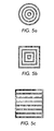
- the printing comprises emitting drops of wax material on the soldermask layer to form nested circles.
- the printing comprises emitting drops of wax material on the soldermask layer to form lines.
- the lines form a grid pattern.
- the lines form nested polygons.
- the developing further comprises removing portions immediately adjacent the underlying material.
- a means is provided to implement the methods.
- the means for forming comprises a printing system operative to emit drops of the wax material.
- FIGURES 1(a)-1(c) illustrate a conventional technique for patterning a soldermask layer
- FIGURE 3 is a flow chart illustrating a method that can be used in the system of FIGURE 2 according to the presently described embodiments;
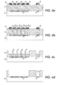
- FIGURE 4(a)-4(d) illustrate a process for patterning a soldermask layer in accordance with the presently described embodiments
- FIGURE 7 illustrates a method for generating a suitable pattern according to the presently described embodiments
- FIGURE 8 illustrates a form of a generated pattern according to the presently described embodiments.
- One advantage is that large areas and small areas can be patterned without loading effect and can be patterned evenly, due to uniform wax lifting. This process allows for runout matching for better registration and is transparent to current developing methods.
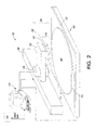
- the printing system 100 includes a stage 102 for supporting (and optionally translating or conveying) a substrate 104, a print assembly 116 mounted to a printing support structure 120, and a computer/workstation 110 that serves as both a system controller and data processor.
- Stage 102 includes a rotational platform 112 that allows the orientation of substrate 104 to be adjusted.
- Print assembly 106 includes a print head 116 (on a rotational fixture) and a camera 118 (having high magnification capabilities) mounted in a rigid mount 120.
- Print head 116 includes one or more ejectors 122 mounted in an ejector base 124. Ejectors 122 are configured to dispense droplets of a printing fluid on substrate 104.
- the printing fluid can comprise a variety of materials, including phase-change materials such as wax or photoresist (to form semiconductor process masks), and colloidal suspensions such as solution-processable electronic (i.e., conducting, semiconducting, or dielectric) materials, and organic or inorganic materials (e.g., to form IC features).
- Substrate 104 can comprise any material on which patterning can be performed, such as a wafer, a glass plate, or even flexible materials such as fabric or plastics.
- ejectors 122 can be in various arrangements and orientations, according to various embodiments of the invention.
- Computer/workstation 110 is configured to receive PCB layout data from a data source 124, and then provide appropriate control signals to printing support structure.
- Data source 124 can comprise any source of layout data, including a networked computer, a layout database connected via a local area network (LAN) or wide area network (WAN), or even a CD-ROM or other removable storage media.
- the control signals provided by computer/workstation 110 control the motion and printing action of the print head as it is translated relative to the substrate. Note that the printing action can be provided by printing support structure, by stage, or by both in combination. Note further that the printing action does not have to involve actual movement of the print head itself, as print head could be held stationary while stage translates the substrate.
- Computer/workstation 110 is also coupled to receive and process imaging data from camera 118. As will be described subsequently, camera 118 can provide both manual and automated calibration capabilities for printing system 100.
- a method 300 according to the presently described embodiments is described. It should be appreciated that this method 300 may be implemented using a variety of different hardware configurations and/or software techniques, including those described in connection with the system 100 shown in Figure 2 . So, for example, software routines that implement various functions of the method may reside in and may be executed by the computer 110.
- the print system 106 may be used to print the contemplated mask pattern, as described in more detail below.
- the method 300 includes a variety of steps, such as coating and baking (or exposing and developing), that may not be implemented using the system of Figure 1 . Implementation of any such steps is accomplished using conventional techniques which require no further explanation than is provided herein. Of course, as explained in more detail below, in one form, the developing will include the removal of the wax pattern and portions of soldermask in accord with the presently described embodiments.
- the printed circuit board is sent to an area or zone wherein analysis and printing functions may take place (at 306).
- the zone may include a printer station that may take a variety of forms, including that shown in Figure 1 .
- the printer station may be a modular unit that can be incorporated within a circuit board assembly process line.
- the printed circuit board is analyzed by the printer station (such as a system 100) using, for example, fiducial marks on the printed circuit board. In this way, the alignment and/or orientation that need to be achieved to print a suitable pattern on the soldermask are determined (at 308).
- the techniques for analyzing fiducials on a printed circuit board are well known in the art.
- the wax pattern and soldermask beneath the wax pattern is suitably removed to expose the desired areas of the circuit board. Portions of the soldermask that are immediately adjacent the soldermask beneath the wax pattern are also removed during the developing. Typically, the exposed areas are those that correspond to copper pads that are useful for electrical connection for the circuit board.
- any material such as other material that can be printed or patterned, that can meet the objectives of the presently described embodiment would be appropriate.
- the material would have similar qualities as wax to the extent that wax serves to block ultraviolet radiation during the exposure process, and thus acts as a blocking material.
- Figure 4(c) shows the combination during the beginning stages of the development process. As can be seen, the wax pattern and significant portions of the uncross-linked soldermask are removed. In one form, the wax pattern is lifted off evenly within about 30 seconds. Note that the cross-linked dams 50 remain at this point in the process.
- the relative dimensions of the components described herein are factors in the implementation of the presently described embodiments.
- the relative dimensions of the dams 50 are a function of the printer capabilities and govern the limitations of the implementations of the presently described embodiments.
- the spacing between the drops is a function of the limits of the printing device.
- the size of the drops can be a function of the printing device that is used.
- the ratio between the thickness of the soldermask and the spacing between the wax drops should be tuned so that the dams 50 are of an appropriate size for removal during development. In this regard, in one form, the ratio between the thickness of the soldermask and the spacing is approximately 4:1. It should be appreciated that ratios in the range of 2:1 and 3:1 may also suffice.
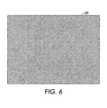
- Figure 7 a flow chart illustrating the technique to generate a corresponding mask pattern to achieve the pattern of Figure 6 is illustrated. Also, Figure 8 shows a decimated image, or an image showing the dot pattern used to achieve the shape, of the image 600.
- the design layer, or image of the printed circuit is rasterized (at 704). From the rasterized image, features of the circuit board for which a pattern is to be generated are selected to be printed (at 706).
Landscapes
- Engineering & Computer Science (AREA)
- Manufacturing & Machinery (AREA)
- Microelectronics & Electronic Packaging (AREA)
- Physics & Mathematics (AREA)
- General Physics & Mathematics (AREA)
- Exposure And Positioning Against Photoresist Photosensitive Materials (AREA)
- Printing Plates And Materials Therefor (AREA)
- Electric Connection Of Electric Components To Printed Circuits (AREA)
- Non-Metallic Protective Coatings For Printed Circuits (AREA)
Applications Claiming Priority (1)
| Application Number | Priority Date | Filing Date | Title |
|---|---|---|---|
| US11/731,689 US8968985B2 (en) | 2007-03-30 | 2007-03-30 | Method and system for patterning a mask layer |
Publications (3)
| Publication Number | Publication Date |
|---|---|
| EP1975699A2 true EP1975699A2 (de) | 2008-10-01 |
| EP1975699A3 EP1975699A3 (de) | 2009-01-21 |
| EP1975699B1 EP1975699B1 (de) | 2016-08-17 |
Family
ID=39615731
Family Applications (1)
| Application Number | Title | Priority Date | Filing Date |
|---|---|---|---|
| EP08151996.9A Ceased EP1975699B1 (de) | 2007-03-30 | 2008-02-27 | Verfahren und System zur Strukturierung einer Maskenschicht |
Country Status (6)
| Country | Link |
|---|---|
| US (1) | US8968985B2 (de) |
| EP (1) | EP1975699B1 (de) |
| JP (1) | JP5128337B2 (de) |
| CN (1) | CN101276143B (de) |
| MY (1) | MY152881A (de) |
| SG (2) | SG146594A1 (de) |
Cited By (1)
| Publication number | Priority date | Publication date | Assignee | Title |
|---|---|---|---|---|
| CN108811358A (zh) * | 2018-06-22 | 2018-11-13 | 赣州中盛隆电子有限公司 | 一种电路板的阻焊工艺 |
Families Citing this family (7)
| Publication number | Priority date | Publication date | Assignee | Title |
|---|---|---|---|---|
| US20090250246A1 (en) * | 2008-04-07 | 2009-10-08 | Andrew Yaung | Solder by numbers, a method and system for populating printed circuit boards |
| US8303832B2 (en) * | 2009-08-17 | 2012-11-06 | Palo Alto Research Center Incorporated | Solid inks for masks for printed circuit boards and other electronic devices |
| US8211617B2 (en) * | 2009-08-17 | 2012-07-03 | Palo Alto Research Center Incorporated | Solid inks for printed masks |
| JP6525500B2 (ja) * | 2014-02-03 | 2019-06-05 | キヤノン株式会社 | パターン形成方法、リソグラフィ装置及び物品の製造方法 |
| CN104355287B (zh) * | 2014-11-18 | 2016-08-24 | 中国科学院半导体研究所 | 一种多功能组合型纳米图形制作方法 |
| CN107960018A (zh) * | 2017-12-22 | 2018-04-24 | 昆山四合电子有限公司 | 一种线路板固化加工工艺 |
| WO2025039208A1 (zh) * | 2023-08-23 | 2025-02-27 | 北京时代全芯存储技术股份有限公司 | 相变材料的光刻及清洗方法 |
Citations (4)
| Publication number | Priority date | Publication date | Assignee | Title |
|---|---|---|---|---|
| US4429027A (en) | 1981-05-21 | 1984-01-31 | E. I. Du Pont De Nemours & Co. | Photoimaging process |
| WO1998051750A1 (en) | 1997-05-16 | 1998-11-19 | Markem Corporation | Hot melt ink |
| EP1251398A2 (de) | 2001-04-19 | 2002-10-23 | Xerox Corporation | Verfahren zum Druck von Ätzmasken, das Phasenwechselmaterialien verwendet |
| US20030112312A1 (en) | 2001-12-13 | 2003-06-19 | Daniel Gelbart | Non-permanent inkjetted flexographic mask |
Family Cites Families (17)
| Publication number | Priority date | Publication date | Assignee | Title |
|---|---|---|---|---|
| JPH04301086A (ja) | 1991-03-29 | 1992-10-23 | Kenseidou Kagaku Kogyo Kk | 細い金属棒表面に微細な溝を有する金属シャフトの製法 |
| US5894036A (en) * | 1997-06-10 | 1999-04-13 | Tylko; Marek K. | Three-dimensional plotter |
| US6742884B2 (en) | 2001-04-19 | 2004-06-01 | Xerox Corporation | Apparatus for printing etch masks using phase-change materials |
| JP2003283111A (ja) | 2002-03-25 | 2003-10-03 | Sumitomo Bakelite Co Ltd | プリント配線板の洗浄方法 |
| US6972261B2 (en) | 2002-06-27 | 2005-12-06 | Xerox Corporation | Method for fabricating fine features by jet-printing and surface treatment |
| US6890050B2 (en) | 2002-08-20 | 2005-05-10 | Palo Alto Research Center Incorporated | Method for the printing of homogeneous electronic material with a multi-ejector print head |
| US7559619B2 (en) | 2002-08-20 | 2009-07-14 | Palo Alto Research Center Incorporated | Digital lithography using real time quality control |
| TW591782B (en) * | 2003-06-19 | 2004-06-11 | Advanced Semiconductor Eng | Formation method for conductive bump |
| US7309563B2 (en) | 2003-12-19 | 2007-12-18 | Palo Alto Research Center Incorporated | Patterning using wax printing and lift off |
| JP4875834B2 (ja) * | 2003-12-24 | 2012-02-15 | ローム・アンド・ハース・エレクトロニック・マテリアルズ,エル.エル.シー. | マスク |
| US7129181B2 (en) | 2004-09-17 | 2006-10-31 | Palo Alto Research Center Incorporated | Sub-resolution gaps generated by controlled over-etching |
| US7384568B2 (en) | 2006-03-31 | 2008-06-10 | Palo Alto Research Center Incorporated | Method of forming a darkfield etch mask |
| US7696096B2 (en) | 2006-10-10 | 2010-04-13 | Palo Alto Research Center Incorporated | Self-aligned masks using multi-temperature phase-change materials |
| US7524015B2 (en) | 2006-12-20 | 2009-04-28 | Palo Alto Research Center Incorporated | Method of printing smooth micro-scale features |
| US8079656B2 (en) | 2006-12-22 | 2011-12-20 | Palo Alto Research Center Incorporated | Method for decimation of images |
| US7835583B2 (en) | 2006-12-22 | 2010-11-16 | Palo Alto Research Center Incorporated | Method of separating vertical and horizontal components of a rasterized image |
| US7926900B2 (en) | 2006-12-22 | 2011-04-19 | Palo Alto Research Center Incorporated | Method of printing with high spot placement accuracy |
-
2007
- 2007-03-30 US US11/731,689 patent/US8968985B2/en active Active
-
2008
- 2008-02-27 EP EP08151996.9A patent/EP1975699B1/de not_active Ceased
- 2008-03-27 MY MYPI20080858 patent/MY152881A/en unknown
- 2008-03-27 JP JP2008083193A patent/JP5128337B2/ja not_active Expired - Fee Related
- 2008-03-28 CN CN 200810090940 patent/CN101276143B/zh not_active Expired - Fee Related
- 2008-03-31 SG SG200802511-6A patent/SG146594A1/en unknown
- 2008-03-31 SG SG10201508031QA patent/SG10201508031QA/en unknown
Patent Citations (4)
| Publication number | Priority date | Publication date | Assignee | Title |
|---|---|---|---|---|
| US4429027A (en) | 1981-05-21 | 1984-01-31 | E. I. Du Pont De Nemours & Co. | Photoimaging process |
| WO1998051750A1 (en) | 1997-05-16 | 1998-11-19 | Markem Corporation | Hot melt ink |
| EP1251398A2 (de) | 2001-04-19 | 2002-10-23 | Xerox Corporation | Verfahren zum Druck von Ätzmasken, das Phasenwechselmaterialien verwendet |
| US20030112312A1 (en) | 2001-12-13 | 2003-06-19 | Daniel Gelbart | Non-permanent inkjetted flexographic mask |
Cited By (1)
| Publication number | Priority date | Publication date | Assignee | Title |
|---|---|---|---|---|
| CN108811358A (zh) * | 2018-06-22 | 2018-11-13 | 赣州中盛隆电子有限公司 | 一种电路板的阻焊工艺 |
Also Published As
| Publication number | Publication date |
|---|---|
| JP5128337B2 (ja) | 2013-01-23 |
| US8968985B2 (en) | 2015-03-03 |
| EP1975699A3 (de) | 2009-01-21 |
| EP1975699B1 (de) | 2016-08-17 |
| US20080241712A1 (en) | 2008-10-02 |
| SG146594A1 (en) | 2008-10-30 |
| MY152881A (en) | 2014-11-28 |
| JP2008257234A (ja) | 2008-10-23 |
| SG10201508031QA (en) | 2015-10-29 |
| CN101276143B (zh) | 2013-05-22 |
| CN101276143A (zh) | 2008-10-01 |
Similar Documents
| Publication | Publication Date | Title |
|---|---|---|
| US8968985B2 (en) | Method and system for patterning a mask layer | |
| JP5064653B2 (ja) | ワックス印刷とリフトオフを使用するパターン生成方法及び印刷システム | |
| KR100964832B1 (ko) | 배선 기판 상에 배선을 형성하는 배선 형성 시스템 및배선 형성 방법 | |
| US8366434B2 (en) | Imprint alignment method, system and template | |
| EP1392091B1 (de) | Verfahren und System zum Drucken von integrierten Schaltungsplänen | |
| TWI273354B (en) | Composite printing | |
| US20050205524A1 (en) | Method of manufacturing tape wiring substrate | |
| KR100880349B1 (ko) | 다층 회로기판 제조용 표시장치 | |
| KR101445914B1 (ko) | 마스크와 워크의 위치 맞춤 방법 | |
| JPH02501427A (ja) | プリント配線板基板のレジストをパターン化する方法 | |
| CN100525582C (zh) | 在印刷电路板上形成电路图案的方法 | |
| JP5178501B2 (ja) | 認識マークを備えたメタルマスク及びその製造方法 | |
| EP1359467A2 (de) | Vorrichtung und Verfahren zum Übertragen eines Musters von einer Maske auf ein Werkstück | |
| KR20020074163A (ko) | 인쇄 회로 기판 제조 시의 비선형 이미지 왜곡 보정 | |
| WO1993019483A1 (en) | Process for fabricating an active matrix circuit | |
| US6954272B2 (en) | Apparatus and method for die placement using transparent plate with fiducials | |
| KR101238631B1 (ko) | Psr 인쇄용 알루미늄 제판 및 그 제조 방법과 이를 이용한 psr 인쇄 방법 | |
| US5254435A (en) | Method of patterning resist | |
| EP1757175B1 (de) | Verfahren und vorrichtung zum präzisen aufbringen von strukturen auf ein substrat | |
| CN100552544C (zh) | 曝光装置和定位方法 | |
| Ehsani et al. | Lasers speed up board production | |
| US6551697B2 (en) | Printed circuit board, method of making same, and photomask for use in the method | |
| JP2001350269A (ja) | 半田印刷用マスクの製造方法 | |
| Thompson et al. | 450mm wafer patterning with jet and flash imprint lithography | |
| JPH06334281A (ja) | プリント配線板 |
Legal Events
| Date | Code | Title | Description |
|---|---|---|---|
| PUAI | Public reference made under article 153(3) epc to a published international application that has entered the european phase |
Free format text: ORIGINAL CODE: 0009012 |
|
| AK | Designated contracting states |
Kind code of ref document: A2 Designated state(s): AT BE BG CH CY CZ DE DK EE ES FI FR GB GR HR HU IE IS IT LI LT LU LV MC MT NL NO PL PT RO SE SI SK TR |
|
| AX | Request for extension of the european patent |
Extension state: AL BA MK RS |
|
| PUAL | Search report despatched |
Free format text: ORIGINAL CODE: 0009013 |
|
| AK | Designated contracting states |
Kind code of ref document: A3 Designated state(s): AT BE BG CH CY CZ DE DK EE ES FI FR GB GR HR HU IE IS IT LI LT LU LV MC MT NL NO PL PT RO SE SI SK TR |
|
| AX | Request for extension of the european patent |
Extension state: AL BA MK RS |
|
| 17P | Request for examination filed |
Effective date: 20090721 |
|
| AKX | Designation fees paid |
Designated state(s): DE FR GB |
|
| 17Q | First examination report despatched |
Effective date: 20090903 |
|
| GRAP | Despatch of communication of intention to grant a patent |
Free format text: ORIGINAL CODE: EPIDOSNIGR1 |
|
| INTG | Intention to grant announced |
Effective date: 20151016 |
|
| GRAS | Grant fee paid |
Free format text: ORIGINAL CODE: EPIDOSNIGR3 |
|
| GRAA | (expected) grant |
Free format text: ORIGINAL CODE: 0009210 |
|
| AK | Designated contracting states |
Kind code of ref document: B1 Designated state(s): DE FR GB |
|
| REG | Reference to a national code |
Ref country code: GB Ref legal event code: FG4D |
|
| REG | Reference to a national code |
Ref country code: DE Ref legal event code: R096 Ref document number: 602008045675 Country of ref document: DE |
|
| REG | Reference to a national code |
Ref country code: FR Ref legal event code: PLFP Year of fee payment: 10 |
|
| REG | Reference to a national code |
Ref country code: DE Ref legal event code: R097 Ref document number: 602008045675 Country of ref document: DE |
|
| PLBE | No opposition filed within time limit |
Free format text: ORIGINAL CODE: 0009261 |
|
| STAA | Information on the status of an ep patent application or granted ep patent |
Free format text: STATUS: NO OPPOSITION FILED WITHIN TIME LIMIT |
|
| 26N | No opposition filed |
Effective date: 20170518 |
|
| REG | Reference to a national code |
Ref country code: FR Ref legal event code: PLFP Year of fee payment: 11 |
|
| PGFP | Annual fee paid to national office [announced via postgrant information from national office to epo] |
Ref country code: GB Payment date: 20200123 Year of fee payment: 13 |
|
| PGFP | Annual fee paid to national office [announced via postgrant information from national office to epo] |
Ref country code: FR Payment date: 20200122 Year of fee payment: 13 |
|
| GBPC | Gb: european patent ceased through non-payment of renewal fee |
Effective date: 20210227 |
|
| PG25 | Lapsed in a contracting state [announced via postgrant information from national office to epo] |
Ref country code: FR Free format text: LAPSE BECAUSE OF NON-PAYMENT OF DUE FEES Effective date: 20210228 Ref country code: GB Free format text: LAPSE BECAUSE OF NON-PAYMENT OF DUE FEES Effective date: 20210227 |
|
| PGFP | Annual fee paid to national office [announced via postgrant information from national office to epo] |
Ref country code: DE Payment date: 20230119 Year of fee payment: 16 |
|
| REG | Reference to a national code |
Ref country code: DE Ref legal event code: R119 Ref document number: 602008045675 Country of ref document: DE |
|
| PG25 | Lapsed in a contracting state [announced via postgrant information from national office to epo] |
Ref country code: DE Free format text: LAPSE BECAUSE OF NON-PAYMENT OF DUE FEES Effective date: 20240903 |
|
| PG25 | Lapsed in a contracting state [announced via postgrant information from national office to epo] |
Ref country code: DE Free format text: LAPSE BECAUSE OF NON-PAYMENT OF DUE FEES Effective date: 20240903 |