EP1975962A1 - Commutateur, en particulier commutateur électromagnétique - Google Patents
Commutateur, en particulier commutateur électromagnétique Download PDFInfo
- Publication number
- EP1975962A1 EP1975962A1 EP07006734A EP07006734A EP1975962A1 EP 1975962 A1 EP1975962 A1 EP 1975962A1 EP 07006734 A EP07006734 A EP 07006734A EP 07006734 A EP07006734 A EP 07006734A EP 1975962 A1 EP1975962 A1 EP 1975962A1
- Authority
- EP
- European Patent Office
- Prior art keywords
- switching device
- receiving device
- receiving
- limiter
- additional element
- Prior art date
- Legal status (The legal status is an assumption and is not a legal conclusion. Google has not performed a legal analysis and makes no representation as to the accuracy of the status listed.)
- Granted
Links
Images



Classifications
-
- H—ELECTRICITY
- H01—ELECTRIC ELEMENTS
- H01H—ELECTRIC SWITCHES; RELAYS; SELECTORS; EMERGENCY PROTECTIVE DEVICES
- H01H50/00—Details of electromagnetic relays
- H01H50/02—Bases; Casings; Covers
- H01H50/021—Bases; Casings; Covers structurally combining a relay and an electronic component, e.g. varistor, RC circuit
-
- H—ELECTRICITY
- H01—ELECTRIC ELEMENTS
- H01H—ELECTRIC SWITCHES; RELAYS; SELECTORS; EMERGENCY PROTECTIVE DEVICES
- H01H71/00—Details of the protective switches or relays covered by groups H01H73/00 - H01H83/00
- H01H71/02—Housings; Casings; Bases; Mountings
- H01H71/0264—Mountings or coverplates for complete assembled circuit breakers, e.g. snap mounting in panel
- H01H71/0271—Mounting several complete assembled circuit breakers together
- H01H2071/0278—Mounting several complete assembled circuit breakers together with at least one of juxtaposed casings dedicated to an auxiliary device, e.g. for undervoltage or shunt trip
Definitions
- the present invention relates to a switching device, in particular an electromagnetic switching device, wherein the switching device has a housing.
- Switching devices in particular electromagnetic switching devices, are used for example in drive and automation technology and are used in conjunction with other components for securing and controlling electrical consumers.
- Switching devices are, for example, relays or contactors.
- Relays are electromagnetic or electromechanical switches. They are used for switching on, off or switching circuits.
- the classic relay is an electromagnetic switch. It consists of a coil with an iron core. If the coil flows through the current, a magnetic field is created. An anchor is tightened, which then presses two contact springs against each other.
- a contactor is an electromagnetically actuated switch. Again, a control current flows through a magnetic coil, wherein the magnetic attraction mechanically actuates a contact which closes the main circuit.
- Contactors have been developed, inter alia, a consumer with high power consumption, such as a motor turn on a hand-operated pushbutton switch with low switching capacity. Basically, a contactor is also a relay, but with much higher switching capacity.
- Overvoltage limiters limit unacceptably high overvoltages, which can be dangerous, for example, to the windings of electric motors, such as high-voltage motors. Such overvoltages can occur when switching devices are used whose switching path solidifies again very quickly after the current zero crossing.
- the housing of overvoltage limiters is made of plastic. Within the housing, for example, capacitors, fixed resistors and voltage-dependent resistors are connected in series. To connect the surge suppressor to a switching device, this has electrically conductive contacts.
- surge arrester to a switching device, in particular to an electromagnetic switching device, such as a contactor, to be retrofitted.
- the surge limiter is mounted on the front of the electromagnetic switching device.
- the mounting of the surge suppressor to one side or to the back of the switching device is not possible or not useful due to the rear side arrangement of the switching device to a fixture, in particular a mounting rail, or due to the lateral connection of several switching device to each other.
- the lateral mounting of an overvoltage limiter consumes space in the control cabinet.
- the present invention has for its object to provide a switching device, in particular an electromagnetic switching device, in which simple and space-optimized overvoltage limiter and / or an additional element, such as a communication module, can be retrofitted.
- a switching device in particular an electromagnetic switching device, in which simple and space-optimized overvoltage limiter and / or an additional element, such as a communication module, can be retrofitted.
- the switchgear dimension should remain unchanged by mounting an overvoltage limiter and / or an additional element to the switching device, regardless of the connection technology.
- the object is achieved by a switching device, in particular an electromagnetic switching device, wherein the switching device has a housing, in which the switching device has at least one receiving device for completely receiving a surge limiter in the housing of the switching device, wherein the receiving device at least one interface for having electrical contact of the surge limiter.
- the at least one receiving device may alternatively or at the same time be configured to completely receive an additional element, in particular a communication module, wherein the at least one interface is designed alternatively or at the same time for the electrical contacting of the additional element, in particular of the communication module.
- Switching devices in the light of the invention may be mechanical or electromagnetic switching devices.
- the switching devices according to the invention electromagnetic switching devices, such as relays or contactors, is.
- the switching device allows a simple and space-optimized retrofitting of a surge limiter and / or an additional element, such as a communication module, to the switching device by means of a so-called neutral interface.
- Space-optimized means that the outer dimensions of the switching device are not changed by the installation of the surge limiter and / or the additional element to the switching device.
- the switching device according to the invention on at least one receiving device.
- the at least one receiving device is designed such that the overvoltage limiter and / or the additional element, in particular the communication module, is completely enclosed by the housing of the switching device after assembly in the at least one receiving device.
- the at least one receiving device has at least one interface for electrical contacting of the overvoltage limiter and / or the additional element. That is, signals can be transmitted via the interface between the electrical components of the switching device, such as a coil, and the overvoltage limiter and / or the additional element.
- the interface is switchgear internally connected to the electrical components of the switching device, in particular the coil
- the core of the invention is that the switching device has at least one receiving device which is arranged within the switching device such that a subsequently mounted overvoltage limiter and / or a subsequently mounted additional element does not change the outer dimensions of the switching device.
- a subsequently mounted overvoltage limiter and / or a subsequently mounted additional element does not change the outer dimensions of the switching device.
- such a switching device can also be extended by an overvoltage limiter and / or an additional element, such as a communication module, when the switching device is fastened to a switchgear unit or a switching device carrier and there is no installation space laterally or downwardly or at the top of the switching device.
- the at least one receiving device is designed to completely accommodate an overvoltage limiter and / or an additional element. That is, the at least one receiving device has at least the shape of the overvoltage limiter to be mounted and / or the additional element, so that they are mounted in the receiving device and there can eino.
- the receiving device may be designed such that it can receive a surge limiter or an additional element. It is also conceivable that the receiving device completely encloses both an overvoltage limiter and an additional element. Also, more than two such components can be accommodated in a receiving device.
- the at least one receiving device can be arranged on the underside or top side of the switching device.
- a switching device in which the at least one receiving device is provided on the front side of the switching device is preferred.
- the front of the switching device is, especially after the attachment of the switching device to a switchgear unit or a switching device carrier, most easily accessible for the subsequent assembly of a surge limiter and / or an additional element.
- the front side is in the light of the invention, the mounting side of the switching device opposite side. On the mounting side, the switching device is fixed to a holder, in particular a switching device carrier.
- a switching device in which the at least one interface of the at least one receiving device is designed for making electrical contact with different surge limiters is particularly versatile.
- a different overvoltage limiter can be mounted in the receiving device.
- one and the same receiving device can be provided in different switching devices, in particular contactors, since these are compatible with different overvoltage limiters as well as with other additional elements.
- Such an interface represents a so-called neutral interface. Since this is compatible for various overvoltage limiter and for other additional elements, the manufacturing costs for interfaces and thus the switching devices can be reduced.
- the at least one interface of the at least one receiving device advantageously has plug contacts for receiving electrically conductive plug-in elements of the overvoltage limiter and / or the additional element.
- Plug contacts provide a secure contact with the interface with the plug-in elements of the surge limiter and / or the additional element.
- plug-in contacts of the interface allow easy insertion of the plug-in elements of the surge limiter and / or an additional element as well as the firm hold of these components at the interface.
- the plug contacts can be designed to receive plug-in elements or for insertion into corresponding plug-in receptacles.
- the surge limiter and / or the additional element can also be screwed into the receiving device or fastened by means of a spring force.
- the attachment is preferably non-positively.
- a switching device in which the at least one receiving device has fastening elements for fastening the overvoltage limiter and / or the additional element in the at least one receiving device ensures a secure hold of the overvoltage limiter and / or the additional element in the receiving device.
- the receiving device may comprise fastening elements in the form of undercuts or recesses, which are designed for receiving and fixing of locking elements of the surge limiter and / or the additional element. But the fasteners also allow easy removal of the surge limiter and / or the additional element from the receiving device.
- the at least one receiving device is designed for the positive reception of the overvoltage limiter and / or the additional element.
- the dimensions of the switching device can be kept low.
- the mounted overvoltage limiter and / or the additional element sits securely in the receiving device due to the positive locking.
- the Receiving device preferably has the shape of the surge limiter or the additional element.
- the receiving device may have a rectangular, oval or round cross-section. Other shapes and cross sections are equally feasible.
- a defined contour and a specific dimension of the width and depth of the receiving device allow the inclusion of a defined surge limiter with just such a contour and a corresponding dimension. The same applies to the additional element.
- the switching device in particular the housing of the switching device, advantageously has at least one cover element for closing the at least one receiving device.
- at least one cover element of the overvoltage limiter and / or the additional element is held securely and firmly in the receiving device.
- the cover member provides the components of the switching device, in particular the mounted surge limiter and the mounted additional element, such as a communication module, further protection against external influences.
- the lid member may be attached to the housing or the receiving device.
- a switching device in which the at least one cover element is pivotally mounted on the switching device, in particular on the housing of the switching device, is arranged. As a result, the cover element is fixedly arranged on the switching device. For mounting the overvoltage limiter and / or the additional element, the cover element is folded up, the overvoltage limiter and / or the additional element is inserted and then the cover element is closed again.
- the cover element may advantageously have an opening or a viewing window. This makes it possible to detect when the cover element is closed, whether an overvoltage limiter and / or an additional element are mounted in the receiving device or not. Furthermore, the operating state of the assembled component can be read, if it has a corresponding display. That is, due to the opening or the viewing window can be controlled be, whether a damping in the switching device is present. This is also possible in the installed state of the switching device, since the cover element and the receiving device is preferably provided on the front side of the switching device.
- the switching device in particular the housing of the switching device, may itself have a display device for checking the function of the overvoltage limiter and / or the additional element.
- the display device may be, for example, a display in the housing of the switching device.
- the at least one interface of the at least one receiving device is preferably formed touch and finger safe. This means that the interface is arranged in the receiving device such that it is not or only very difficult to access for a fitter.
- the surge limiter and / or the additional element are themselves enveloped by a plastic sheath, so that they are safe to touch.
- a switching device which has a display device for displaying the at least one interface.
- the display device can advantageously be provided on the housing of the switching device or on the at least one receiving device.
- a fitter can immediately recognize how the surge limiter and / or the additional element must be mounted in the receiving device of the switching device.
- the display device may have a coding, by means of which the installer recognizes the correct mounting variant.
- a corresponding coding is advantageously also provided on the overvoltage limiter and / or the additional element. This will ensure the proper and correct installation of the surge suppressor and / or the additional element facilitates.
- a faulty equipment of the switching device is not possible, since the exact installation of an overvoltage limiter or a communication module is specified by the display device. For example, it can be displayed that a communication module can only be mounted in the receiving device if there is no damping.
- overvoltage limiter various components can be used.
- a diode, a varistor or an RC element can be used for damping the coil.
- the mountable communication module may have a communication electronics, which is connected to a control electronics of the switching device.
- the communication module may communicate with a communication unit provided on a switchgear carrier. Via the communication unit and the communication module, an electrical control of the switching device according to the invention is possible.
- the transfer of signals to the electronics in the communication module is preferably carried out via a bus connector or by a fürdringungsAuthtechnik a bus directly to the communication module.
- the additional element may further preferably be designed as a diagnostic and communication module.
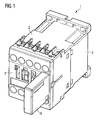
- FIG. 1 a known switching device 1 is shown. Outside on the front side 3 of the housing 2 of the switching device, a high-voltage limiter 10 is attached to the damping of the coil of the switching device 1. By attaching the surge suppressor 10 outside on the front side 3, the dimensions of the switching device 1 have been increased. This leads to the disadvantage if there is no space for external connection of an overvoltage limiter 10. This can quickly be the case when a switchgear cabinet is so tight that such external attachment is not possible due to lack of space.
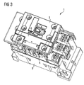
- the FIG. 2 also shows a known switching device 1.
- This switching device 1 has no way to a damping of the coil, ie a surge suppressor 10 to assemble.
- the subsequent installation of an overvoltage limiter 10 is therefore already not possible because the switching device is fixed with its back to a switching device carrier and on the sides of another switching device can be attached. Since the switching devices 1 are arranged in a control cabinet usually side by side in rows, a subsequent installation of a surge limiter 10 on the sides of the switching device 1 is not possible.
- each with a plurality of switching devices 1 are arranged very close to each other in the cabinet, the subsequent installation of a surge limiter 10 at the top or bottom of a switching device 1 is difficult to implement, since access to the top or bottom a switching device 1 is often blocked by lines of the switching device 1 itself or other switching devices 1.
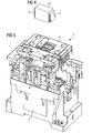
- an inventive switching device 1 is shown.
- This has on the front side 3 a cover element 6, which covers the receiving device 4 according to the invention.
- openings 7 are provided which allow a view into the interior of the receiving device 4. That is, through the openings 7 can be seen whether an overvoltage limiter and / or an additional element, such as a communication module, is / are mounted in the receiving device or not.
- the receiving device 4 can be viewed through the openings 7.
- FIG. 4 shows a retrofittable surge limiter 10. This has fasteners 12 for mounting the surge limiter 10 in the receiving device 4 of the switching device 1.
- the receiving device 4 of the switching device 1 is in FIG. 5 shown. This sits directly under the lid member 6 on the front side 3 of the switching device 1.
- the cover member 6 is plugged in this embodiment of the switching device 1 on the receiving device 4, so that it is protected from external influences.
- openings 7 are provided through which a view into the receiving device 4 can be made to determine whether and which component 10, 20 is seated in the receiving device 4.
- the cover element 6 and the receiving device 4 are provided on the front side 3 of the switching device 1 and the housing 2 of the switching device 1, since the front 3 is best accessible, in particular, when the switching device 1 is part of a switchgear unit and fixed to a switching device carrier.
- an overvoltage limiter 10 is shown, the form-fitting manner in the receiving device 4 of the switching device 1, as in the FIG. 7 shown, can be mounted.
- the overvoltage limiter 10 has fortifications 12 for secure attachment in the receiving device 4 of the switching device 1.
- the FIG. 7 shows a switching device 1 with a pivotally mounted cover member 6, wherein it is in an open state.
- the now visible receiving device 4 allows the subsequent, in particular positive, mounting of the surge limiter 10 according to FIG. 6 ,
- the overvoltage limiter 10 is completely received in the receiving device 4, so that the outer dimensions of the switching device 1 after installation of the surge limiter 10 remain unchanged.
- the cover element 6 is closed, so that it can only be detected through the openings 7 that it sits in the receiving device 4.
- the FIG. 8 shows an additional element 20 in the form of a communication module.
- This communication module has plug-in elements 21 for contacting a provided in the receiving device 4 of the switching device 1, not shown, neutral Interface on.
- the interface and the receiving device 4 may be designed such that they can accommodate different surge limiter 10 and other additional elements 20, such as a communication module. It can be provided that either an overvoltage limiter 10 or an additional element 20 can be mounted in the receiving device 4 of the switching device 1. But it is also possible that both an overvoltage limiter 10 and an additional element 20 can be fastened simultaneously.
- FIG. 9 shows a perspective view of a switching device 1 with receiving device 4 for a communication module 20.
- the receiving device 4 is covered by the lid member 6.
Landscapes
- Physics & Mathematics (AREA)
- Electromagnetism (AREA)
- Emergency Protection Circuit Devices (AREA)
- Electronic Switches (AREA)
- Shielding Devices Or Components To Electric Or Magnetic Fields (AREA)
Priority Applications (3)
| Application Number | Priority Date | Filing Date | Title |
|---|---|---|---|
| AT07006734T ATE434826T1 (de) | 2007-03-30 | 2007-03-30 | Schaltgerät, insbesondere elektromagnetisches schaltgerät |
| EP07006734A EP1975962B1 (fr) | 2007-03-30 | 2007-03-30 | Commutateur, en particulier commutateur électromagnétique |
| DE502007000939T DE502007000939D1 (de) | 2007-03-30 | 2007-03-30 | Schaltgerät, insbesondere elektromagnetisches Schaltgerät |
Applications Claiming Priority (1)
| Application Number | Priority Date | Filing Date | Title |
|---|---|---|---|
| EP07006734A EP1975962B1 (fr) | 2007-03-30 | 2007-03-30 | Commutateur, en particulier commutateur électromagnétique |
Publications (2)
| Publication Number | Publication Date |
|---|---|
| EP1975962A1 true EP1975962A1 (fr) | 2008-10-01 |
| EP1975962B1 EP1975962B1 (fr) | 2009-06-24 |
Family
ID=38050906
Family Applications (1)
| Application Number | Title | Priority Date | Filing Date |
|---|---|---|---|
| EP07006734A Active EP1975962B1 (fr) | 2007-03-30 | 2007-03-30 | Commutateur, en particulier commutateur électromagnétique |
Country Status (3)
| Country | Link |
|---|---|
| EP (1) | EP1975962B1 (fr) |
| AT (1) | ATE434826T1 (fr) |
| DE (1) | DE502007000939D1 (fr) |
Cited By (1)
| Publication number | Priority date | Publication date | Assignee | Title |
|---|---|---|---|---|
| DE102017215271A1 (de) * | 2017-08-31 | 2019-02-28 | Seg Automotive Germany Gmbh | Relais, insbesondere einer Startvorrichtung, mit einer weiteren elektrischen Baueinheit |
Citations (5)
| Publication number | Priority date | Publication date | Assignee | Title |
|---|---|---|---|---|
| DE3503292A1 (de) * | 1985-01-31 | 1986-08-07 | Siemens AG, 1000 Berlin und 8000 München | Anordnung zum ankoppeln einer hilfsschalteranordnung |
| EP0453918A2 (fr) * | 1990-04-27 | 1991-10-30 | Siemens Aktiengesellschaft | Module auxiliaire pour appareil de commutation électromagnétique |
| DE19618736A1 (de) * | 1995-05-10 | 1996-11-14 | Mitsubishi Electric Corp | Anschlußblock und Steuereinheit mit Anschlußblock |
| WO1999054980A1 (fr) * | 1998-04-17 | 1999-10-28 | Siemens Aktiengesellschaft | Module antiparasites |
| DE102005026714B3 (de) * | 2005-06-09 | 2006-12-14 | Siemens Ag | Schutzeinrichtung mit einer Schutzschaltereinheit und mit einer Überspannungsschutzeinheit |
-
2007
- 2007-03-30 EP EP07006734A patent/EP1975962B1/fr active Active
- 2007-03-30 DE DE502007000939T patent/DE502007000939D1/de active Active
- 2007-03-30 AT AT07006734T patent/ATE434826T1/de active
Patent Citations (5)
| Publication number | Priority date | Publication date | Assignee | Title |
|---|---|---|---|---|
| DE3503292A1 (de) * | 1985-01-31 | 1986-08-07 | Siemens AG, 1000 Berlin und 8000 München | Anordnung zum ankoppeln einer hilfsschalteranordnung |
| EP0453918A2 (fr) * | 1990-04-27 | 1991-10-30 | Siemens Aktiengesellschaft | Module auxiliaire pour appareil de commutation électromagnétique |
| DE19618736A1 (de) * | 1995-05-10 | 1996-11-14 | Mitsubishi Electric Corp | Anschlußblock und Steuereinheit mit Anschlußblock |
| WO1999054980A1 (fr) * | 1998-04-17 | 1999-10-28 | Siemens Aktiengesellschaft | Module antiparasites |
| DE102005026714B3 (de) * | 2005-06-09 | 2006-12-14 | Siemens Ag | Schutzeinrichtung mit einer Schutzschaltereinheit und mit einer Überspannungsschutzeinheit |
Cited By (1)
| Publication number | Priority date | Publication date | Assignee | Title |
|---|---|---|---|---|
| DE102017215271A1 (de) * | 2017-08-31 | 2019-02-28 | Seg Automotive Germany Gmbh | Relais, insbesondere einer Startvorrichtung, mit einer weiteren elektrischen Baueinheit |
Also Published As
| Publication number | Publication date |
|---|---|
| DE502007000939D1 (de) | 2009-08-06 |
| ATE434826T1 (de) | 2009-07-15 |
| EP1975962B1 (fr) | 2009-06-24 |
Similar Documents
| Publication | Publication Date | Title |
|---|---|---|
| EP2546856B1 (fr) | Baguette pour fusibles NH | |
| EP0830810B1 (fr) | Unite d'appareillages de commutation convernant aux telecommunications | |
| EP1529302B2 (fr) | Commutateur electrique | |
| EP1917672B1 (fr) | Systeme de connexion comprenant un appareil de commutation electromagnetique, en particulier un contacteur electromagnetique, et un connecteur | |
| DE3525085A1 (de) | Einrichtung fuer ein kraftfahrzeug | |
| DE202014009245U1 (de) | Schaltgerät sowie Schaltgeräteanordnung | |
| DE102007027522B3 (de) | Schaltgerät | |
| EP2720325B1 (fr) | Prise commutable | |
| DE202014101491U1 (de) | Busfähiges aneinanderreihbares Anschluss- und/oder Funktionsmodul | |
| EP3510676A1 (fr) | Module de protection contre les surtensions pour un connecteur modulaire | |
| EP2315318B1 (fr) | Prise électrique à contact protégé | |
| DE102008020348A1 (de) | Stromverteilung für Fahrzeuge, insbesondere Luftfahrzeuge | |
| DE102013111925A1 (de) | Thermostateinheit | |
| EP1975962B1 (fr) | Commutateur, en particulier commutateur électromagnétique | |
| EP2383765B1 (fr) | Relais doté d'une commutation de sécurité intégrée | |
| DE10361452A1 (de) | Anordnung zum Befestigen von elektrischen und/oder elektronischen Bauteilen, insbesondere Leistungsbauteilen, an einer Platine und Gehäuse hiermit | |
| EP4068329B1 (fr) | Dispositif destiné à l'agencement sur barres de distribution comprenant un appareil de commutation et un composant électronique | |
| EP2020067B1 (fr) | Dispositif de mise hors circuit ou mise en circuit automatique d'un récepteur électrique | |
| EP2140470B1 (fr) | Module avec extension automatique d'un circuit de controle | |
| WO2009010111A1 (fr) | Distributeur de courant | |
| DE60124210T2 (de) | Einrichtung zur elektrischen Verbindung von zwei elektrischen Schaltgeräten wie z.B. eines elektrischen Schutzschalters und eines zugeordneten angesteuerten Schalters sowie an eine solche Einrichtung angepasstes elektrisches Schaltgerät | |
| WO2008028434A1 (fr) | Module complémentaire destiné à être monté sur un appareillage d'installation et combinaison du module complémentaire avec l'appareillage d'installation | |
| DE102020212249B4 (de) | Schaltschrank mit einem Kabelverlegekasten | |
| DE10146502A1 (de) | Elektrische Installationsverteilung | |
| EP2064721A1 (fr) | Appareillage de commutation avec prelevement de voie de courant principale integre |
Legal Events
| Date | Code | Title | Description |
|---|---|---|---|
| PUAI | Public reference made under article 153(3) epc to a published international application that has entered the european phase |
Free format text: ORIGINAL CODE: 0009012 |
|
| 17P | Request for examination filed |
Effective date: 20070822 |
|
| AK | Designated contracting states |
Kind code of ref document: A1 Designated state(s): AT BE BG CH CY CZ DE DK EE ES FI FR GB GR HU IE IS IT LI LT LU LV MC MT NL PL PT RO SE SI SK TR |
|
| AX | Request for extension of the european patent |
Extension state: AL BA HR MK RS |
|
| GRAP | Despatch of communication of intention to grant a patent |
Free format text: ORIGINAL CODE: EPIDOSNIGR1 |
|
| GRAS | Grant fee paid |
Free format text: ORIGINAL CODE: EPIDOSNIGR3 |
|
| GRAL | Information related to payment of fee for publishing/printing deleted |
Free format text: ORIGINAL CODE: EPIDOSDIGR3 |
|
| GRAS | Grant fee paid |
Free format text: ORIGINAL CODE: EPIDOSNIGR3 |
|
| GRAA | (expected) grant |
Free format text: ORIGINAL CODE: 0009210 |
|
| AKX | Designation fees paid |
Designated state(s): AT BE BG CH CY CZ DE DK EE ES FI FR GB GR HU IE IS IT LI LT LU LV MC MT NL PL PT RO SE SI SK TR |
|
| AK | Designated contracting states |
Kind code of ref document: B1 Designated state(s): AT BE BG CH CY CZ DE DK EE ES FI FR GB GR HU IE IS IT LI LT LU LV MC MT NL PL PT RO SE SI SK TR |
|
| REG | Reference to a national code |
Ref country code: GB Ref legal event code: FG4D Free format text: NOT ENGLISH |
|
| REG | Reference to a national code |
Ref country code: CH Ref legal event code: EP |
|
| REG | Reference to a national code |
Ref country code: IE Ref legal event code: FG4D Free format text: LANGUAGE OF EP DOCUMENT: GERMAN |
|
| REF | Corresponds to: |
Ref document number: 502007000939 Country of ref document: DE Date of ref document: 20090806 Kind code of ref document: P |
|
| PG25 | Lapsed in a contracting state [announced via postgrant information from national office to epo] |
Ref country code: FI Free format text: LAPSE BECAUSE OF FAILURE TO SUBMIT A TRANSLATION OF THE DESCRIPTION OR TO PAY THE FEE WITHIN THE PRESCRIBED TIME-LIMIT Effective date: 20090624 Ref country code: LT Free format text: LAPSE BECAUSE OF FAILURE TO SUBMIT A TRANSLATION OF THE DESCRIPTION OR TO PAY THE FEE WITHIN THE PRESCRIBED TIME-LIMIT Effective date: 20090624 |
|
| PG25 | Lapsed in a contracting state [announced via postgrant information from national office to epo] |
Ref country code: SI Free format text: LAPSE BECAUSE OF FAILURE TO SUBMIT A TRANSLATION OF THE DESCRIPTION OR TO PAY THE FEE WITHIN THE PRESCRIBED TIME-LIMIT Effective date: 20090624 Ref country code: PL Free format text: LAPSE BECAUSE OF FAILURE TO SUBMIT A TRANSLATION OF THE DESCRIPTION OR TO PAY THE FEE WITHIN THE PRESCRIBED TIME-LIMIT Effective date: 20090624 Ref country code: SE Free format text: LAPSE BECAUSE OF FAILURE TO SUBMIT A TRANSLATION OF THE DESCRIPTION OR TO PAY THE FEE WITHIN THE PRESCRIBED TIME-LIMIT Effective date: 20090924 Ref country code: LV Free format text: LAPSE BECAUSE OF FAILURE TO SUBMIT A TRANSLATION OF THE DESCRIPTION OR TO PAY THE FEE WITHIN THE PRESCRIBED TIME-LIMIT Effective date: 20090624 |
|
| NLV1 | Nl: lapsed or annulled due to failure to fulfill the requirements of art. 29p and 29m of the patents act | ||
| PG25 | Lapsed in a contracting state [announced via postgrant information from national office to epo] |
Ref country code: IS Free format text: LAPSE BECAUSE OF FAILURE TO SUBMIT A TRANSLATION OF THE DESCRIPTION OR TO PAY THE FEE WITHIN THE PRESCRIBED TIME-LIMIT Effective date: 20091024 Ref country code: ES Free format text: LAPSE BECAUSE OF FAILURE TO SUBMIT A TRANSLATION OF THE DESCRIPTION OR TO PAY THE FEE WITHIN THE PRESCRIBED TIME-LIMIT Effective date: 20091005 Ref country code: EE Free format text: LAPSE BECAUSE OF FAILURE TO SUBMIT A TRANSLATION OF THE DESCRIPTION OR TO PAY THE FEE WITHIN THE PRESCRIBED TIME-LIMIT Effective date: 20090624 Ref country code: CZ Free format text: LAPSE BECAUSE OF FAILURE TO SUBMIT A TRANSLATION OF THE DESCRIPTION OR TO PAY THE FEE WITHIN THE PRESCRIBED TIME-LIMIT Effective date: 20090624 |
|
| REG | Reference to a national code |
Ref country code: IE Ref legal event code: FD4D |
|
| PG25 | Lapsed in a contracting state [announced via postgrant information from national office to epo] |
Ref country code: SK Free format text: LAPSE BECAUSE OF FAILURE TO SUBMIT A TRANSLATION OF THE DESCRIPTION OR TO PAY THE FEE WITHIN THE PRESCRIBED TIME-LIMIT Effective date: 20090624 Ref country code: NL Free format text: LAPSE BECAUSE OF FAILURE TO SUBMIT A TRANSLATION OF THE DESCRIPTION OR TO PAY THE FEE WITHIN THE PRESCRIBED TIME-LIMIT Effective date: 20090624 |
|
| PG25 | Lapsed in a contracting state [announced via postgrant information from national office to epo] |
Ref country code: PT Free format text: LAPSE BECAUSE OF FAILURE TO SUBMIT A TRANSLATION OF THE DESCRIPTION OR TO PAY THE FEE WITHIN THE PRESCRIBED TIME-LIMIT Effective date: 20091024 Ref country code: BG Free format text: LAPSE BECAUSE OF FAILURE TO SUBMIT A TRANSLATION OF THE DESCRIPTION OR TO PAY THE FEE WITHIN THE PRESCRIBED TIME-LIMIT Effective date: 20090924 |
|
| PG25 | Lapsed in a contracting state [announced via postgrant information from national office to epo] |
Ref country code: DK Free format text: LAPSE BECAUSE OF FAILURE TO SUBMIT A TRANSLATION OF THE DESCRIPTION OR TO PAY THE FEE WITHIN THE PRESCRIBED TIME-LIMIT Effective date: 20090624 Ref country code: IE Free format text: LAPSE BECAUSE OF FAILURE TO SUBMIT A TRANSLATION OF THE DESCRIPTION OR TO PAY THE FEE WITHIN THE PRESCRIBED TIME-LIMIT Effective date: 20090624 |
|
| PLBE | No opposition filed within time limit |
Free format text: ORIGINAL CODE: 0009261 |
|
| STAA | Information on the status of an ep patent application or granted ep patent |
Free format text: STATUS: NO OPPOSITION FILED WITHIN TIME LIMIT |
|
| 26N | No opposition filed |
Effective date: 20100325 |
|
| BERE | Be: lapsed |
Owner name: SIEMENS A.G. Effective date: 20100331 |
|
| PG25 | Lapsed in a contracting state [announced via postgrant information from national office to epo] |
Ref country code: MC Free format text: LAPSE BECAUSE OF NON-PAYMENT OF DUE FEES Effective date: 20100331 Ref country code: GR Free format text: LAPSE BECAUSE OF FAILURE TO SUBMIT A TRANSLATION OF THE DESCRIPTION OR TO PAY THE FEE WITHIN THE PRESCRIBED TIME-LIMIT Effective date: 20090925 |
|
| PG25 | Lapsed in a contracting state [announced via postgrant information from national office to epo] |
Ref country code: BE Free format text: LAPSE BECAUSE OF NON-PAYMENT OF DUE FEES Effective date: 20100331 |
|
| PG25 | Lapsed in a contracting state [announced via postgrant information from national office to epo] |
Ref country code: IT Free format text: LAPSE BECAUSE OF NON-PAYMENT OF DUE FEES Effective date: 20100330 |
|
| PG25 | Lapsed in a contracting state [announced via postgrant information from national office to epo] |
Ref country code: MT Free format text: LAPSE BECAUSE OF FAILURE TO SUBMIT A TRANSLATION OF THE DESCRIPTION OR TO PAY THE FEE WITHIN THE PRESCRIBED TIME-LIMIT Effective date: 20090624 |
|
| REG | Reference to a national code |
Ref country code: CH Ref legal event code: PL |
|
| GBPC | Gb: european patent ceased through non-payment of renewal fee |
Effective date: 20110330 |
|
| PG25 | Lapsed in a contracting state [announced via postgrant information from national office to epo] |
Ref country code: CH Free format text: LAPSE BECAUSE OF NON-PAYMENT OF DUE FEES Effective date: 20110331 Ref country code: LI Free format text: LAPSE BECAUSE OF NON-PAYMENT OF DUE FEES Effective date: 20110331 Ref country code: DE Free format text: LAPSE BECAUSE OF NON-PAYMENT OF DUE FEES Effective date: 20111001 |
|
| PG25 | Lapsed in a contracting state [announced via postgrant information from national office to epo] |
Ref country code: GB Free format text: LAPSE BECAUSE OF NON-PAYMENT OF DUE FEES Effective date: 20110330 |
|
| PG25 | Lapsed in a contracting state [announced via postgrant information from national office to epo] |
Ref country code: CY Free format text: LAPSE BECAUSE OF FAILURE TO SUBMIT A TRANSLATION OF THE DESCRIPTION OR TO PAY THE FEE WITHIN THE PRESCRIBED TIME-LIMIT Effective date: 20090624 |
|
| PG25 | Lapsed in a contracting state [announced via postgrant information from national office to epo] |
Ref country code: HU Free format text: LAPSE BECAUSE OF FAILURE TO SUBMIT A TRANSLATION OF THE DESCRIPTION OR TO PAY THE FEE WITHIN THE PRESCRIBED TIME-LIMIT Effective date: 20091225 Ref country code: LU Free format text: LAPSE BECAUSE OF NON-PAYMENT OF DUE FEES Effective date: 20100330 |
|
| PG25 | Lapsed in a contracting state [announced via postgrant information from national office to epo] |
Ref country code: TR Free format text: LAPSE BECAUSE OF FAILURE TO SUBMIT A TRANSLATION OF THE DESCRIPTION OR TO PAY THE FEE WITHIN THE PRESCRIBED TIME-LIMIT Effective date: 20090624 |
|
| REG | Reference to a national code |
Ref country code: AT Ref legal event code: MM01 Ref document number: 434826 Country of ref document: AT Kind code of ref document: T Effective date: 20120330 |
|
| PG25 | Lapsed in a contracting state [announced via postgrant information from national office to epo] |
Ref country code: AT Free format text: LAPSE BECAUSE OF NON-PAYMENT OF DUE FEES Effective date: 20120330 |
|
| PG25 | Lapsed in a contracting state [announced via postgrant information from national office to epo] |
Ref country code: RO Free format text: LAPSE BECAUSE OF FAILURE TO SUBMIT A TRANSLATION OF THE DESCRIPTION OR TO PAY THE FEE WITHIN THE PRESCRIBED TIME-LIMIT Effective date: 20090624 |
|
| REG | Reference to a national code |
Ref country code: FR Ref legal event code: PLFP Year of fee payment: 10 |
|
| REG | Reference to a national code |
Ref country code: FR Ref legal event code: PLFP Year of fee payment: 11 |
|
| REG | Reference to a national code |
Ref country code: FR Ref legal event code: PLFP Year of fee payment: 12 |
|
| P01 | Opt-out of the competence of the unified patent court (upc) registered |
Effective date: 20230510 |
|
| PGFP | Annual fee paid to national office [announced via postgrant information from national office to epo] |
Ref country code: DE Payment date: 20250714 Year of fee payment: 20 |
|
| PGFP | Annual fee paid to national office [announced via postgrant information from national office to epo] |
Ref country code: IT Payment date: 20260324 Year of fee payment: 20 |
|
| PGFP | Annual fee paid to national office [announced via postgrant information from national office to epo] |
Ref country code: FR Payment date: 20260316 Year of fee payment: 20 |