EP1976104A2 - Convertisseur de courant continu indirect avec un transformateur ayant des enroulements plans - Google Patents
Convertisseur de courant continu indirect avec un transformateur ayant des enroulements plans Download PDFInfo
- Publication number
- EP1976104A2 EP1976104A2 EP08005065A EP08005065A EP1976104A2 EP 1976104 A2 EP1976104 A2 EP 1976104A2 EP 08005065 A EP08005065 A EP 08005065A EP 08005065 A EP08005065 A EP 08005065A EP 1976104 A2 EP1976104 A2 EP 1976104A2
- Authority
- EP
- European Patent Office
- Prior art keywords
- coil
- primary coil
- primary
- transformer
- current
- Prior art date
- Legal status (The legal status is an assumption and is not a legal conclusion. Google has not performed a legal analysis and makes no representation as to the accuracy of the status listed.)
- Granted
Links
Images


Classifications
-
- H—ELECTRICITY
- H02—GENERATION; CONVERSION OR DISTRIBUTION OF ELECTRIC POWER
- H02M—APPARATUS FOR CONVERSION BETWEEN AC AND AC, BETWEEN AC AND DC, OR BETWEEN DC AND DC, AND FOR USE WITH MAINS OR SIMILAR POWER SUPPLY SYSTEMS; CONVERSION OF DC OR AC INPUT POWER INTO SURGE OUTPUT POWER; CONTROL OR REGULATION THEREOF
- H02M7/00—Conversion of AC power input into DC power output; Conversion of DC power input into AC power output
- H02M7/003—Constructional details, e.g. physical layout, assembly, wiring or busbar connections
-
- H—ELECTRICITY
- H01—ELECTRIC ELEMENTS
- H01F—MAGNETS; INDUCTANCES; TRANSFORMERS; SELECTION OF MATERIALS FOR THEIR MAGNETIC PROPERTIES
- H01F27/00—Details of transformers or inductances, in general
- H01F27/28—Coils; Windings; Conductive connections
- H01F27/2804—Printed windings
-
- H—ELECTRICITY
- H01—ELECTRIC ELEMENTS
- H01F—MAGNETS; INDUCTANCES; TRANSFORMERS; SELECTION OF MATERIALS FOR THEIR MAGNETIC PROPERTIES
- H01F27/00—Details of transformers or inductances, in general
- H01F27/28—Coils; Windings; Conductive connections
- H01F27/2847—Sheets; Strips
-
- H—ELECTRICITY
- H02—GENERATION; CONVERSION OR DISTRIBUTION OF ELECTRIC POWER
- H02M—APPARATUS FOR CONVERSION BETWEEN AC AND AC, BETWEEN AC AND DC, OR BETWEEN DC AND DC, AND FOR USE WITH MAINS OR SIMILAR POWER SUPPLY SYSTEMS; CONVERSION OF DC OR AC INPUT POWER INTO SURGE OUTPUT POWER; CONTROL OR REGULATION THEREOF
- H02M3/00—Conversion of DC power input into DC power output
- H02M3/22—Conversion of DC power input into DC power output with intermediate conversion into AC
- H02M3/24—Conversion of DC power input into DC power output with intermediate conversion into AC by static converters
- H02M3/28—Conversion of DC power input into DC power output with intermediate conversion into AC by static converters using discharge tubes with control electrode or semiconductor devices with control electrode to produce the intermediate AC
- H02M3/325—Conversion of DC power input into DC power output with intermediate conversion into AC by static converters using discharge tubes with control electrode or semiconductor devices with control electrode to produce the intermediate AC using devices of a triode or a transistor type requiring continuous application of a control signal
- H02M3/335—Conversion of DC power input into DC power output with intermediate conversion into AC by static converters using discharge tubes with control electrode or semiconductor devices with control electrode to produce the intermediate AC using devices of a triode or a transistor type requiring continuous application of a control signal using semiconductor devices only
- H02M3/33569—Conversion of DC power input into DC power output with intermediate conversion into AC by static converters using discharge tubes with control electrode or semiconductor devices with control electrode to produce the intermediate AC using devices of a triode or a transistor type requiring continuous application of a control signal using semiconductor devices only having several active switching elements
- H02M3/33571—Half-bridge at primary side of an isolation transformer
-
- H—ELECTRICITY
- H02—GENERATION; CONVERSION OR DISTRIBUTION OF ELECTRIC POWER
- H02M—APPARATUS FOR CONVERSION BETWEEN AC AND AC, BETWEEN AC AND DC, OR BETWEEN DC AND DC, AND FOR USE WITH MAINS OR SIMILAR POWER SUPPLY SYSTEMS; CONVERSION OF DC OR AC INPUT POWER INTO SURGE OUTPUT POWER; CONTROL OR REGULATION THEREOF
- H02M3/00—Conversion of DC power input into DC power output
- H02M3/22—Conversion of DC power input into DC power output with intermediate conversion into AC
- H02M3/24—Conversion of DC power input into DC power output with intermediate conversion into AC by static converters
- H02M3/28—Conversion of DC power input into DC power output with intermediate conversion into AC by static converters using discharge tubes with control electrode or semiconductor devices with control electrode to produce the intermediate AC
- H02M3/325—Conversion of DC power input into DC power output with intermediate conversion into AC by static converters using discharge tubes with control electrode or semiconductor devices with control electrode to produce the intermediate AC using devices of a triode or a transistor type requiring continuous application of a control signal
- H02M3/335—Conversion of DC power input into DC power output with intermediate conversion into AC by static converters using discharge tubes with control electrode or semiconductor devices with control electrode to produce the intermediate AC using devices of a triode or a transistor type requiring continuous application of a control signal using semiconductor devices only
- H02M3/33569—Conversion of DC power input into DC power output with intermediate conversion into AC by static converters using discharge tubes with control electrode or semiconductor devices with control electrode to produce the intermediate AC using devices of a triode or a transistor type requiring continuous application of a control signal using semiconductor devices only having several active switching elements
- H02M3/33573—Full-bridge at primary side of an isolation transformer
-
- H—ELECTRICITY
- H02—GENERATION; CONVERSION OR DISTRIBUTION OF ELECTRIC POWER
- H02M—APPARATUS FOR CONVERSION BETWEEN AC AND AC, BETWEEN AC AND DC, OR BETWEEN DC AND DC, AND FOR USE WITH MAINS OR SIMILAR POWER SUPPLY SYSTEMS; CONVERSION OF DC OR AC INPUT POWER INTO SURGE OUTPUT POWER; CONTROL OR REGULATION THEREOF
- H02M3/00—Conversion of DC power input into DC power output
- H02M3/22—Conversion of DC power input into DC power output with intermediate conversion into AC
- H02M3/24—Conversion of DC power input into DC power output with intermediate conversion into AC by static converters
- H02M3/28—Conversion of DC power input into DC power output with intermediate conversion into AC by static converters using discharge tubes with control electrode or semiconductor devices with control electrode to produce the intermediate AC
- H02M3/325—Conversion of DC power input into DC power output with intermediate conversion into AC by static converters using discharge tubes with control electrode or semiconductor devices with control electrode to produce the intermediate AC using devices of a triode or a transistor type requiring continuous application of a control signal
- H02M3/335—Conversion of DC power input into DC power output with intermediate conversion into AC by static converters using discharge tubes with control electrode or semiconductor devices with control electrode to produce the intermediate AC using devices of a triode or a transistor type requiring continuous application of a control signal using semiconductor devices only
- H02M3/337—Conversion of DC power input into DC power output with intermediate conversion into AC by static converters using discharge tubes with control electrode or semiconductor devices with control electrode to produce the intermediate AC using devices of a triode or a transistor type requiring continuous application of a control signal using semiconductor devices only in push-pull configuration
-
- H—ELECTRICITY
- H01—ELECTRIC ELEMENTS
- H01F—MAGNETS; INDUCTANCES; TRANSFORMERS; SELECTION OF MATERIALS FOR THEIR MAGNETIC PROPERTIES
- H01F27/00—Details of transformers or inductances, in general
- H01F27/28—Coils; Windings; Conductive connections
- H01F27/2871—Pancake coils
-
- H—ELECTRICITY
- H01—ELECTRIC ELEMENTS
- H01F—MAGNETS; INDUCTANCES; TRANSFORMERS; SELECTION OF MATERIALS FOR THEIR MAGNETIC PROPERTIES
- H01F27/00—Details of transformers or inductances, in general
- H01F27/28—Coils; Windings; Conductive connections
- H01F27/2876—Cooling
-
- H—ELECTRICITY
- H01—ELECTRIC ELEMENTS
- H01F—MAGNETS; INDUCTANCES; TRANSFORMERS; SELECTION OF MATERIALS FOR THEIR MAGNETIC PROPERTIES
- H01F27/00—Details of transformers or inductances, in general
- H01F27/34—Special means for preventing or reducing unwanted electric or magnetic effects, e.g. no-load losses, reactive currents, harmonics, oscillations, leakage fields
- H01F27/343—Preventing or reducing surge voltages; oscillations
-
- H—ELECTRICITY
- H02—GENERATION; CONVERSION OR DISTRIBUTION OF ELECTRIC POWER
- H02M—APPARATUS FOR CONVERSION BETWEEN AC AND AC, BETWEEN AC AND DC, OR BETWEEN DC AND DC, AND FOR USE WITH MAINS OR SIMILAR POWER SUPPLY SYSTEMS; CONVERSION OF DC OR AC INPUT POWER INTO SURGE OUTPUT POWER; CONTROL OR REGULATION THEREOF
- H02M3/00—Conversion of DC power input into DC power output
- H02M3/01—Resonant DC/DC converters
Definitions
- the present invention relates to a switching supply such as a DC/DC converter.
- a conventional switching supply such as a DC/DC converter appears in Japanese Patent No. 2,629,999 , for example.
- This DC/DC converter uses a transformer and generally has a primary coil and a secondary coil wound around one core.
- the present invention was conceived in view of this problem and an object of the present invention is to provide a switching supply such as a DC/DC converter which exhibits superior power conversion efficiency.
- the switching supply according to the present invention involves a switching supply which comprises an inverter circuit which is connected to a primary coil group of the transformer and a rectification/smoothing circuit which is connected to a secondary coil group of the transformer.
- the transformer comprises a core that comprises a first through section and a second through section which is spatially separate from the first through section and constitutes a magnetic circuit together with the first through section; the first through section passes through the inside of at least one coil of the primary coil group and at least one coil of the secondary coil group; the second through section passes through the inside of the remaining coils of the primary and secondary coil groups; the coil group that follows one loop direction of the magnetic circuit comprises a first coil group which has a primary coil and a secondary coil that are magnetically coupled and, subsequently to the first coil group, a second coil group which has a primary coil and a secondary coil that are magnetically coupled.
- the first through section comprises primary and secondary coils which pass therethrough and a coil group is also provided in the second through section.
- the surface area over which the coil group extends within a plane which is perpendicular to the through sections is greater than in the case where all of the coils are provided in a single through section. Therefore, because the heat radiation characteristic is improved in the case of a wide surface area, the cooling efficiency of the transformer improves.
- the switching supply comprises a plurality of coil groups which are magnetically coupled to one another in particular, because it is difficult to move the heat produced in the plurality of coil groups through heat conduction, heat transfer, or heat radiation, a heat radiation structure of this kind is effective.
- the coils of the first or second coil group are preferably arranged in the one loop direction of the magnetic circuit in the following order: secondary coil, primary coil, and secondary coil, or primary coil, secondary coil, and primary coil. In this case, because the symmetry of the coil arrangement is maintained for the center coils, the current distribution of the coil groups is made uniform.
- the partial AC resistance is preferably increased with the object of suppressing the output ringing of the switching supply.
- the primary coil of the first coil group and the primary coil of the second coil group are connected in series and the AC resistance of the primary coil of the first coil group and the AC resistance of the primary coil of the second coil group are preferably set such that one is alternately higher than the other in sync with the switching of the inverter circuit.
- the switching supply such as a DC/DC converter of the present invention has improved cooling efficiency and the power conversion efficiency is superior.
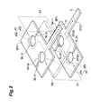
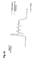
- Fig. 1 is a perspective view of the DC/DC converter
- Fig. 2 is a perspective view of platelike members
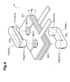
- Fig. 3 is a connection diagram which shows, in perspective form, the connected relationship between primary coils 42 and 43 and secondary coils 45 and 46 which are provided on the wiring substrate;
- Fig. 4 is a perspective view of the transformer 4
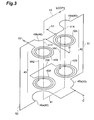
- Fig. 5 is a perspective view of a wiring substrate PB
- Fig. 6 is the circuit diagram of the DC/DC converter
- Fig. 7 is a circuit diagram of the DC/DC converter
- Fig. 8 is a circuit diagram of the DC/DC converter
- Fig. 9 is a circuit diagram of the DC/DC converter of this embodiment.
- Fig. 10 is a structural diagram of the DC/DC converter
- Fig. 11 is an equivalent circuit diagram of the primary coil of the transformer
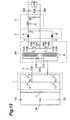
- Fig. 12 is a circuit diagram of the DC/DC converter according to a comparative example
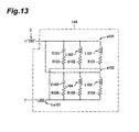
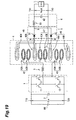
- Fig. 13 is an equivalent circuit diagram of the primary coil of the transformer
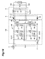
- Fig. 14 is a circuit diagram which serves to illustrate the operation of the DC/DC converter
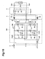
- Fig. 15 is another circuit diagram which serves to illustrate the operation of the DC/DC converter
- Fig. 16 is a circuit diagram of a waveform diagram of the output AC voltage of the transformer
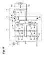
- Fig. 17 is a circuit diagram which serves to illustrate the operation of the DC/DC converter
- Fig. 18 is another circuit diagram which serves to illustrate the operation of the DC/DC converter
- Fig. 19 is a circuit diagram of the DC/DC converter according to one modified example.
- Fig. 20 is a circuit diagram of the DC/DC converter according to another modified example.
- Fig. 21 is a circuit diagram of the DC/DC converter according to another modified example.
- Fig. 22 is a circuit diagram of the DC/DC converter according to another modified example.
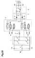
- Fig. 23 is a circuit diagram of the DC/DC converter according to the embodiment.
- Fig. 24 is a structural diagram of the DC/DC converter
- Fig. 25 is an equivalent circuit diagram of the primary coil of the transformer
- Fig. 26 is a circuit diagram which serves to illustrate the operation of the DC/DC converter
- Fig. 27 is another circuit diagram which serves to illustrate the operation of the DC/DC converter
- Fig. 28 is a circuit diagram of the DC/DC converter according to a modified example
- Fig. 29 is a circuit diagram of the DC/DC converter according to another modified example.
- Fig. 30 is a circuit diagram of the DC/DC converter according to another modified example.
- Fig. 31 is a circuit diagram of the DC/DC converter according to another modified example.
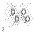
- Fig. 32 shows the arrangement of the transformer 4 of the DC/DC converter
- Fig. 33 shows the arrangement of the transformer 4 of the DC/DC converter.
- Fig. 1 is a perspective view of the DC/DC converter.
- the DC/DC converter comprises an inverter circuit 1 which is connected to a primary coil group of a transformer 4, and a rectification circuit 5 and smoothing circuit 6 which are connected to a secondary coil group of the transformer 4.
- the rectification circuit 5 and smoothing circuit 6 taken as a whole constitute a rectification/smoothing circuit.
- An input smoothing capacitor 2 and a current detection current transformer 2A are provided next to the power source HB of the inverter circuit 1.
- the inverter circuit 1 has a plurality of switching elements 11, 12, 13, and 14 disposed between the high-voltage power line and low-voltage power line of power source HB.
- the switching elements 11 and 12 which constitute a first switching element array are connected in series and the switching elements 13 and 14 which constitute a second switching element array are also in series.
- the first switching element array and second switching element array are arranged in parallel between the power lines.
- the switching elements 11, 12, 13, and 14 comprise a field effect transistor and a parasitic diode and a capacitor are attached between the source and drain of each field effect transistor so that the power source voltage is applied with a reverse bias.
- the connection point XA between the switching element 11 and switching element 12 is connected to the first input terminal X1 of the transformer 4 via a resonant inductor 3.
- the connection point XB between the switching element 13 and switching element 14 is connected to the other input terminal X2 of the transformer 4.
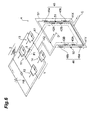
- the upper platelike member SP1 comprises two openings SP1A and SP1B and comprises slits SL1a and SL1b which extend from the side walls of openings SP1A and SP1B to the outside edge of the platelike member SP1.
- the directions from the slits SL1a and SL1b to the openings SP1A and SP1B are mutually opposite.
- Wiring substrate PB on whose upper and lower sides the helical primary coil is printed is interposed via an insulating layer IF between the platelike members SP1 and SP2.
- the platelike member SP1 and platelike member SP2 are electrically connected via diodes 51 and 52 which constitute the rectification circuit 5.
- the direction of the wire portion linking the centers of the openings SPA1 and SPA2 is the X axis direction.
- the anode of diode 51 is connected to an edge which intersects one direction of the X axis of lower platelike member SP2 and the cathode is connected to an edge which intersects one direction of the X axis of upper platelike member SP1.
- the anode of diode 52 is connected to an edge which intersects the other direction of the X axis of the lower platelike member SP2 and the cathode is connected to the edge which intersects the other direction of the X axis of the upper platelike member SP1.
- the diode 51 connects a plurality of diodes 51a, 51b, 51c, and 51d in parallel and diode 52 connects a plurality of diodes 52a, 52b, 52c, and 52d in parallel.
- a current I/O section SP1T extends from the side which intersects the axis (Y axis assumed) which is orthogonal to the X axis of the platelike member so as to protrude in the Y axis direction from the main body section and, on the surface of the lower platelike member SP2, a current I/O section SP2T extends from the side which intersects the Y axis so as to protrude in the Y axis direction from the main body section.
- opening SP1B is located on the extension line in the Y axis negative direction of the current I/O section SP1T and opening SP2B (See Fig. 2 ) is located on the extension line in the Y axis negative direction of the current I/O section SP2T.
- a through-hole in the openings SP1A and SP1B of transformer 4 passes through as far as the lower side of the transformer 4 and the core 41 passes through the inside of both through-holes.
- Core 41 forms a loop in plane XZ and constitutes a magnetic circuit.
- the member in the Z axis positive direction of core 41 comprises a leg portion 41A 1 which passes through the inside of the first through-hole, a leg portion 41A 2 which passes through the inside of the other through-hole, and a connection 41A 3 which connects leg portion 41A 1 and leg portion 41A 2 , and forms an inverted U-shaped magnetic body core 41 A.
- the member in the Z axis negative direction of core 41 comprises a leg portion 41B 1 which passes through the inside of the first through-hole, a leg portion 41B 2 which passes through the inside of the other through-hole, and a connection 41B 3 which connects leg portion 41B 1 and leg portion 41B 2 , and forms a U-shaped magnetic body core 41B.
- the leading edges of the leg portions of both of the magnetic body cores 41A and 41B face one another and make contact with one another.
- the leg portions 41A 1 and 41B 1 of the magnetic body cores which pass through the insides of the through-holes constitute a first through section 41X (See Fig. 3 ) and the leg portions 41A 2 and 41B 2 constitute a second through section 41Y (See Fig. 3 ).
- the first through section 41X and second through section 41Y are spatially separate along the X axis.
- Fig. 2 is a perspective view of the platelike members.
- the lower platelike member SP2 has a shape which is obtained by inverting the top and bottom of the upper platelike member SP1 and comprises two openings SP2A and SP2B. Furthermore, the lower platelike member SP2 comprises slits SL2a and SL2b which extend from the side wall of the openings SP2A and SP2B to the outside edge of the platelike member SP2. The directions from the slits SL2a and SL2b to the openings SP2A and SP2B are mutually opposite.
- the current branches off to follow either one of the current path S1 and the current path S2. Which branch path the current follows depends on the direction of the current entering the primary coil.
- the current path S 1 comprises a path along the partial arc of the opening SP2B of the platelike member SP2 which prescribes a part 45b of the secondary coil 45 and a path which extends along the partial arc of the opening SP1A of the platelike member SP1 which prescribes the remaining part 45a of the secondary coil 45 and the current that passes through part 45a flows out to the downstream circuit via the upper current I/O section SP1T.
- the secondary coil 45 is constituted split into upper and lower platelike members.
- the current path S 1 avoids slits SL2b and SL1a which extend in mutually opposite directions from the upper and lower platelike members SP2 and SP1 and describes an arc which flows only in a rotary direction.
- the current path S2 comprises a path along a partial arc of opening SP2A of platelike member SP2 which prescribes a part 46a of the secondary coil 46 and a path along a partial arc of opening SP1B of platelike member SP1 which prescribes the remaining part 46b of the secondary coil 46 and the current that passes through part 46b flows out to the downstream circuit via the upper current I/O section SP1T.
- the secondary coil 46 is also constituted split into upper and lower platelike members.
- the current path S2 avoids slits SL2a and SL1b which extend in mutually opposite directions from the upper and lower platelike members SP2 and SP1 and describes an arc which flows only in a rotary direction.
- the secondary coil comprises a pair of conductive platelike members (or conductive thin films) which are provided so as to sandwich the primary coil and slits which extend from the opening are formed in the respective platelike members, the respective platelike members are electrically connected, a secondary coil is formed by the current path such that the current which flows between the platelike members avoids the slits and which passes through the periphery of the opening.
- This structure is a simple structure.
- diodes 51 and 52 are interposed between the platelike members SP1 and SP2 which constitute half coils.
- the rotational direction of the current can be freely set if the positions of each slit are changed.
- the wiring substrate PB provided with the primary coil is located between the platelike member SP1 and the platelike member SP2.
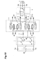
- Fig. 3 is a connection diagram which shows, in perspective form, the connected relationship between primary coils 42 and 43 and secondary coils 45 and 46 which are provided on the wiring substrate.
- the first through section 41X of the core 41 passes through the secondary coil 45a, primary coil 42A, primary coil 42B, and secondary coil 45b which are arranged in order starting from the top.
- the second through section 41 Y of the core 41 passes through the secondary coil 46b, the primary coil 43B, the primary coil 43A, and the secondary coil 46a which are arranged in order starting from the top.
- These respective coils are planar coils.
- the innermost end of the primary coil 42A and the innermost end of the primary coil 42B are electrically connected via a via-contact VA1 and, in cases where current is flowing in the coils from one direction, the directions of the currents flowing in both coils are then equal.
- the outermost end of the primary coil 42B is electrically connected to the outermost end of the adjacent primary coil 43B via the printed wiring PW.
- the innermost end of the primary coil 43B is electrically connected to the innermost end of the primary coil 43B via a via-contact VA2 and, in cases where current flows from one direction in these coils, the directions of the currents flowing in both coils are then equal.
- the center coils 42A and 42B can also be regarded as one coil 42 and the center coils 43A and 43B can also be regarded as one coil 43.
- Fig. 4 is a perspective view of transformer 4.
- Core 41 is constituted by an inverted U-shaped magnetic body 41 A and a U-shaped magnetic body core 41B and the respective leg portions 41A 1 , 41A 2 , 41B 1 , and 41B 2 constitute cylinders and are located in through-holes directly below openings SP1A and SP1B.
- the connection sections 41A 3 and 41B 3 are opposite the respective platelike members SP1 and SP2 and, in cases where the magnetic body cores 41A and 41B are combined, cover the area between the opening of the respective platelike members SP1 and SP2.
- a wide surface area which is not covered by the magnetic body cores 41A and 41B exists in the platelike members SP 1 and SP2 of the transformer 4.
- the transformer 4 comprises a core 41 which comprises the first through section 41X and a second through section 41 Y which constitutes a magnetic circuit together with the first through section 41X and at least one coil (42A, for example) of the primary coil group and at least one coil (45a (45), for example) of the secondary coil group are wound around the first through section 41X while the remaining coils of the primary and secondary coils are wound around the second through section 41Y.
- the coil group that follows the one loop direction (LOOP1: See Fig. 3 , for example) of the magnetic circuit comprises a first coil group (45b, 42B, 42A, 45a: See Fig.
- first through section 41X and second through section 41Y pass through the insides of the coils wound therearound.
- the surface area over which the coil group extends within a plane which is perpendicular to the through sections 41X and 41Y is greater than in the case where all of the coils are provided in a single through section.
- the surface area which is not covered by the magnetic body cores 41A and 41B of the platelike members SP1 and SP2 increases. In cases where the surface area of the members is large, the heat radiation characteristic is enhanced. Hence, the cooling efficiency of the transformer 4 improves. In cases where there is a plurality of coil groups which are magnetically coupled to one another in particular, because the heat produced in the plurality of coil groups is easily confined, such a heat radiation structure is effective.
- Fig. 5 is a perspective view of the wiring substrate PB.
- the wiring substrate PB comprises an insulating substrate PB, a planar coils 42A and 43A applied to the upper surface of the substrate PB, and planar coils 42B and 43A applied to the lower side of the substrate PB.
- the upper and lower coils electrically connect the substrate PB via contacts VA1 and VA2 in via holes which pass through the thickness direction.
- Fig. 6 is a circuit diagram of the DC/DC converter.
- the secondary coil 45, the primary coils 42A and 42B and the secondary coil 45b are arranged next to the first through section 41X which comprises a magnetic body core in order starting from the top and the secondary coil 46a, the primary coils 43A and 43B, and the secondary coil 46b are arranged next to the second through section 41 Y which comprises a magnetic body core in order starting from the bottom.
- the secondary coil is of the same polarity as the primary coil and a current flows in the secondary coil in the reverse direction from the current path P1 of the primary coil. That is, at this time, the current that flows in from terminal C passes through diode 51 and current path S 1 and comes out at terminal D.
- Fig. 7 is a circuit diagram of the DC/DC converter.
- the secondary coil has the same polarity as that of the primary coil and a current flows in the secondary coil in the opposite direction from the current path P2 of the primary coil. That is, the current that flows in from terminal C passes through the diode 52 and current path S2 and comes out at terminal D.
- Fig. 8 is a circuit diagram of the DC/DC converter.
- the circuit diagram is the same as the circuit diagram of the DC/DC converter.
- the secondary coil 45a, the primary coils 42A and 42B, the secondary coil 45b, the secondary coil 46a, the primary coils 43A and 43B, and the secondary coil 46b are arranged in order starting from the top along the primary current path P1.
- the direction of the current which is to flow through the secondary coils 45a and 45b is the opposite direction from the forward current of the diode 51. Hence, current does not flow in the secondary coils 45a and 45b.
- the AC resistance of the primary coils 42A and 42B is higher in relative terms than the AC resistance of the primary coils 43A and 43B.
- the outputs of the secondary coils are smoothed by a smoothing circuit 6 which comprises an LC filter and are supplied as direct current to load L.
- the primary coils 42A and 42B of the first coil group (45b, 42B, 42A, 45a) and the primary coils 43A and 43B of the secondary coil group (46a, 43B, 43A, 46a) are connected in series and the AC resistance of the primary coils 42A and 42B of the first coil group and the AC resistance of the primary coils 43A and 43B of the second coil group are set such that one AC resistance is alternately higher than the other in sync with the switching of inverter circuit 1.
- a primary coil with a high AC resistance is connected in series with a primary coil with a low AC resistance, because AC resistance converges the oscillation within the coil group, ringing of the output can be suppressed. Therefore, the power conversion efficiency of the DC/DC converter rises further.
- zero volt switching control may be performed by the inverter circuit 1 and, in this case, the loss of the switching elements 11, 12, 13, and 14 can be suppressed.
- the coils of the first or second coil group are preferably arranged in the one loop direction of the magnetic circuit in the following order: secondary coil, primary coil, and secondary coil, or primary coil, secondary coil, and primary coil.
- the current distribution of the coil groups is made uniform.
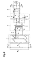
- Fig. 9 represents the circuit constitution of the DC/DC converter, where the positions of the diodes 51 and 52 differ from those mentioned earlier in that same have moved directly in front of node D.
- Fig. 10 shows the structure of the transformer in the DC/DC converter of Fig. 9 in an enlarged form.
- This DC/DC converter functions as a DC/DC converter which converts a high-voltage DC input voltage Vin which is supplied by power source HB that comprises a high-voltage battery, for example, into a lower DC output voltage Vout and supplies the lower DC output voltage Vout to load L which comprises a low voltage battery, for example, and is a secondary center-tapped DC/DC converter.
- the DC/DC converter comprises a primary high-voltage power line L1H, an inverter circuit 1 (switching circuit) and a smoothing capacitor 2 which are provided between the primary high-voltage power line L1H and a low-voltage power line L1L, a transformer 4 which is constituted comprising a primary coil 44 which comprises a primary coil 42 and a primary coil 43 which are connected in series to one another and a secondary coil 47 which comprises a secondary coil 45 and a secondary coil 46 which are connected in series to one another, and a resonance coil (inductor) 3 which is provided between the inverter circuit 1 and transformer 4.
- the coil may also be wound.
- An input terminal T10 is provided on primary high-voltage power line L1H and an input terminal T20 is provided on primary low-voltage power line L1L. These input terminals T10 and T20 are connected to the output terminal of power source HB.
- An output terminal T30 is provided on an output line L0 which is the high-voltage line of smoothing circuit 6 and an output terminal T40 is provided on ground line LG which is the low-voltage line of smoothing circuit 6.
- the output terminals T30 and T40 are connected to the I/O terminal of load L.
- the inverter circuit 1 is a single-phase inverter circuit which converts DC input voltage Vin which is output by power source HB into a substantially rectangular waveform single-phase AC voltage.
- the inverter circuit 1 is a full bridge-type switching circuit in which four switching elements 11, 12, 13, and 14 which are each driven by switching signals that are supplied by the control circuit (not shown) are full bridge-connected.
- Elements such as a MOS-FET (Metal Oxide Semiconductor Field Effect Transistor) or an IGBT (Insulated Gate Bipolar Transistor), for example, are employed as the switching elements.
- the switching element 11 is provided between one end of the resonant inductor 3 and the primary high-voltage power line L1H and switching element 12 is provided between one end of the resonant inductor 3 and the primary low-voltage power line L1L.
- Switching element 13 is provided between one end of the primary coil 43 of the transformer 4 and the primary high-voltage power line L1H and switching element 14 is provided between one end of the primary coil 43 and the primary low-voltage power line L1L.
- the resonant inductor 3 constitutes a resonant circuit together with at least one of the parasitic capacitances of the switching elements 11, 12, 13, and 14 and uses the resonance characteristic to reduce the power loss produced as a result of the ON and OFF action of the switching elements.
- the resonant inductor 3 may be constituted by actually disposing a coil part or may instead (also) be constituted by using a Series inductance which includes the leakage inductance of the transformer 4 and the wiring and so forth.
- the transformer 4 is a magnetic element which is magnetically coupled as a result of being wound on core 41 so that the primary coil 44 (primary coil group) which comprises primary coil 42 (primary first coil group) and primary coil 43 (primary second coil group) which are connected in series to one another, and the secondary coil 47 (secondary coil group) which comprises secondary coil 45 (secondary first coil group) and secondary coil 46 (secondary second coil group) which are connected in series to one another have polarities of the same orientation.
- the transformer 4 is a step-down transformer and the number of windings of the secondary coil 45 and secondary coil 46 is smaller than the number of windings of the primary coil 44.
- the magnitude of the voltage step-down is decided by the ratio between the number of windings of the primary coil 44 and the number of windings of each of the secondary coil 45 and secondary coil 46.
- a U-shape type In addition to combining a U-shape type with a U-shape type for core 41 as mentioned earlier, a combination of a U-shape type and an I-shape type can be employed, in which case the core 41 has an annular magnetic path.
- the secondary coil 45 comprises a secondary coil 45A (secondary first subcoil group) and a secondary coil 45B (secondary second subcoil group) which are connected to one another in parallel.
- the secondary coil 46 comprises a secondary coil 46A (secondary third subcoil group) and a secondary coil 46B (secondary fourth subcoil group) which are connected to one another in parallel.
- the secondary coil 45A, secondary coil 45B, secondary coil 46A and secondary coil 46B are wound around the core 41.
- One end of the secondary coil 45 is connected to the anode of the diode 51 and the other end of the secondary coil 45 is connected to center tap (terminal) C. Meanwhile, one end of the secondary coil 46 is connected to the anode of a diode 52 (described subsequently) while the other end of the secondary coil 46 is connected to center tap C. Center tap C is connected to the output terminal T40 via a ground line LG. That is, the secondary winding of the transformer 4 is a center tap-type connection.
- the secondary coil 45 and secondary coil 46 are driven in mutually opposite phases with time division by the rectification circuit 5.
- the primary coil 42 comprises a primary coil 42A (primary first subcoil group) and a primary coil 42B (primary second subcoil group) which are connected to one another in series.
- the primary coil 42A and primary coil 42B are each wound around the core 41 three times.
- the primary coil 42 is sandwiched between the secondary coil 45A and the secondary coil 45B, the primary coil 42A is disposed close to the secondary coil 45A, and the primary coil 42B is disposed close to the secondary coil 45B.
- the primary coil 42 is disposed closer to the secondary coil 45 than to the secondary coil 46.
- the primary coil 43 comprises primary coil 43A (primary third subcoil group) and primary coil 43B (primary fourth subcoil group) which are connected in series to one another.
- the primary coils 43A and primary coil 43B are each wound three times around the core 41.
- the primary coil 43 is sandwiched between secondary coil 46A and secondary coil 46B, the primary coil 43A is disposed adjacent to the secondary coil 46A, and the primary coil 43B is disposed adjacent to the secondary coil 46B.
- the primary coil 43 is disposed closer to the secondary coil 46 than to the secondary coil 45.
- the transformer 4 comprises a structure in which the primary coils (primary coils 42 and 43) and the secondary coils (secondary coils 45 and 46) are alternately stacked (in a sandwich shape) and the primary coil 42 and primary coil 43 in which the current flows in the same direction are close to one another on the same axis.
- the respective coils of the transformer 4 has an arrangement of coils which follows a loop in one direction of the magnetic path in which the coils are stacked in the following order: secondary coil 45A (secondary first subcoil group), primary coil 42A (primary first subcoil group), primary coil 42B (primary second subcoil group), secondary coil 45B (secondary second subcoil group), secondary coil 46A (secondary third subcoil group), primary coil 43A (primary third subcoil group), primary coil 43B (primary fourth subcoil group), and secondary coil 46B (secondary fourth subcoil group).
- the stacked structure of the transformer 4 is symmetrical along the loop.
- the primary coil 42 and primary coil 43 are connected to the inverter circuit 1 so that the direction of the current which flows into the primary coil 42 and primary coil 43 changes depending on the operation of the inverter circuit 1. More specifically, one end of the primary coil 42 is connected to connection point XA between the switching element 11 and switching element 12 via the resonant inductor 3; the other end of the primary coil 42 is connected to one end of the primary coil 43; and the other end of the primary coil 43 is connected to connection point XB between switching element 13 and switching element 14.
- Primary coil 42A, primary coil 42B, primary coil 43A, primary coil 43B, secondary coil 45, secondary coil 45B, secondary coil 46A, and secondary coil 46B may also be isolated from one another by air or may be isolated from one another through the interposition of an insulating sheet (not shown).
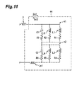
- the primary coil 44 which comprises the primary coil 42 and primary coil 43 can be represented by an equivalent circuit such as the one shown in Fig. 11 .
- this equivalent circuit is a circuit in which a circuit a1, circuit a2, and inductance Le1 are connected in series to one another.
- Circuit a1 is constituted by connecting an inductance L1 and resistance R1 which are connected in series to one another, an inductance L2 and resistance R2 which are connected in series to one another, and a line capacitance C1 and resistance R3 which are connected in series to one another, in parallel to one another.
- Circuit a2 is constituted by connecting an inductance L3 and resistance R4 which are connected in series to one another, an inductance L4 and resistance R5, which are connected in series to one another, and a line capacitance C2 and resistance R6, which are connected in series to one another, in parallel to one another.
- the inductance L1 is the inductance of the primary coil 42 when the transformer 4 is an ideal transformer and resistance R1 is the resistance of the primary coil 42 when the transformer 4 is an ideal transformer.
- the inductance L2 is the excitation inductance of the primary coil 42 and resistance R2 is the AC resistance part of the primary coil 42.
- the line capacitance C 1 is the total capacitance of the line capacitance in the primary coil 42 and the line capacitance of the primary coil 42 and secondary coils 45 and 46 and the resistance R3 is the AC resistance part of the primary coil 42.
- the inductance L3 is the inductance of the primary coil 43 when the transformer 4 is an ideal transformer and the resistance R4 is the resistance of the primary coil 43 when the transformer 4 is an ideal transformer.
- the inductance L4 is the excitation inductance of the primary coil 43 and the resistance R5 is the AC resistance part of the primary coil 43.
- the line capacitance C2 is the total capacitance of the line capacitance of the primary coil 43 and the line capacitances of the primary coil 43 and secondary coils 45 and 46 and the resistance R6 is the AC resistance component of the primary coil 43.
- the inductance Le1 is the excitation inductance of the transformer 4.
- the rectification circuit 5 is a single-phase full wave rectification-type circuit which comprises a pair of diodes 51 (first rectifying element) and a diode 52 (second rectifying element).
- the anode of the diode 51 is connected to one end of the secondary coil 45 and the cathode of the diode 51 is connected to connection point D.
- the anode of the diode 52 is connected to one end of the secondary coil 46 and the cathode of the diode 52 is connected to connection point D.
- Connection point D is connected to the output terminal T30 via smoothing circuit 6.
- the rectification circuit 5 drives the secondary coil 45 and secondary coil 46 in mutually opposite phases with time division.
- the smoothing circuit 6 is constituted comprising a choke coil 61 and a smoothing capacitor 62 and generates a DC output voltage Vout by smoothing the DC voltage rectified by the rectification circuit 5 and supplies the DC output voltage Vout from the output terminals T30 and T40 to the load L.
- the inverter circuit 1 can also be driven through zero volt switching control, for example.
- the DC/DC converter converts (steps down) the DC input voltage Vin which was supplied by the power source into the DC output voltage Vout and supplies the DC output voltage Vout thus converted to the load.
- the primary coil 144 of a transformer 104 is constituted by connecting a primary coil 142 and a primary coil 145 in parallel and differs from the primary coil 44 of this embodiment in this respect.
- the primary coil 142 of the comparative example has a primary coil 142A and a primary coil 142B which are connected in series to one another.
- the primary coil 142A and primary coil 142B are each wound six times around core 41 and are stacked in that order starting from the top. From the perspective of arranging the magnitudes of the voltage step-downs by the transformer between the embodiment and comparative example, the number of windings of the primary coil 142 is two times the number of windings of the primary coil 42, that is, twelve windings.
- the primary coil 142 is sandwiched between the secondary coil 45A and the secondary coil 45B and the primary coil 142A is disposed close to the secondary coil 45A and the primary coil 142B is disposed close to the secondary coil 45B. As a result, the primary coil 142 is disposed closer to the secondary coil 45 than the secondary coil 46.
- the primary coil 143 of the comparative example comprises a primary coil 143A and primary coil 143B which are connected in series to one another.
- the primary coil 143A and primary coil 143B are wound three times around core 41 and stacked in that order starting from the top. From the perspective of arranging the voltage step-downs by the transformer between the embodiment and comparative example, the number of windings of the primary coil 143 is two times the number of windings of the primary coil 43, that is, twelve windings.
- the primary coil 143 is sandwiched between the secondary coil 46A and the secondary coil 46B and the primary coil 143A is disposed close to the secondary coil 46A and the primary coil 143B is disposed close to the secondary coil 46B. As a result, the primary coil 143 is disposed closer to the secondary coil 46 than the secondary coil 45.
- the primary coil of the transformer 104 of the comparative example that is, the primary coil 144 which comprises the primary coil 142 and primary coil 143 can be represented by an equivalent circuit of the kind shown in Fig. 13 .
- the equivalent circuit is a circuit in which a circuit in which circuit a101 and a circuit a 102 are connected in parallel to one another and the inductance Le101 are connected in series to one another.
- Circuit a101 is constituted by connecting an inductance L101 and resistance R101 which are connected in series to one another, an inductance L102 and resistance R102 which are connected in series to one another, and a line capacitance C101 and resistance R103 which are connected in series to one another, in parallel to one another.
- Circuit a102 is constituted by connecting an inductance L103 and resistance R104 which are connected in series to one another, an inductance L104 and resistance R105 which are connected in series to one another, and a line capacitance C102 and resistance R106 which are connected in series to one another, in parallel to one another.
- the inductance L101 is the inductance of the primary coil 142 when the transformer 104 is an ideal transformer and resistance R101 is the resistance of the primary coil 142 when the transformer 104 is an ideal transformer.
- the inductance L102 is the excitation inductance of the primary coil 142.
- the resistance R102 is the AC resistance component of the primary coil 142.
- the line capacitance C101 is the total capacitance of the line capacitance in the primary coil 142 and the line capacitances of the primary coil 142 and secondary coils 45 and 46 and the resistance R103 is the AC resistance component of the primary coil 142.
- the inductance L103 is the inductance of the primary coil 143 when the transformer 104 is an ideal transformer and the resistance R104 is the resistance of the primary coil 143 when the transformer 104 is an ideal transformer.
- the inductance L104 is the excitation inductance of the primary coil 143 and the resistance R105 is the AC resistance component of the primary coil 143.
- the line capacitance C102 is the total capacitance of the line capacitance in the primary coil 143 and the line capacitances of the primary coil 143 and the secondary coils 45 and 46 and the resistance R106 is the AC resistance component of the primary coil 143.
- the inductance Le 101 is the excitation inductance of the transformer 104.
- a current Iin11 flows in the primary coil 142 and a current Iin12 flows in the primary coil 143.
- the primary coil 142 is disposed closer to the secondary coil 45 in which the current flows and is therefore tightly magnetically coupled to the secondary coil 45.
- the primary coil 142 and secondary coil 45 have, based on the principles of the transformer, currents which flow in mutually opposite directions. Therefore, in comparison with a case where coil groups which have the same current flow direction are adjacent in the primary coil 142, the AC resistance drops because the influence of the proximity effect drops. Accordingly, a relatively large current flows in the primary coil 142.
- the primary coil 143 is disposed farther from the secondary coil 45 in which the current flows and is loosely magnetically coupled to the secondary coil 45.
- the primary coil 143 is disposed relatively close to the secondary coil 46 in which the current does not flow, the AC resistance in the primary coil 143 is higher as a result of the proximity effect than that of the primary coil 142. Only a relatively small current therefore flows in the primary coil 143.
- the primary coil 143 is disposed closer to the secondary coil 46 in which the current flows and is therefore relatively tightly magnetically coupled to the secondary coil 46.
- the primary coil 143 and secondary coil 46 have, based on the principles of a transformer, currents which flow in mutually opposite directions. Therefore, in comparison with a case where coil groups which have the same current flow direction are adjacent in the primary coil 143, the AC resistance drops because the influence of the proximity effect drops. Accordingly, a relatively large current flows in the primary coil 143.
- the primary coil 142 is disposed farther from the secondary coil 46 in which the current flows and is therefore relatively loosely magnetically coupled to the secondary coil 46.
- the primary coil 142 is disposed relatively close to the secondary coil 45 in which the current does not flow, the AC resistance in the primary coil 142 is higher as a result of the proximity effect than that of the primary coil 143. Only a relatively small current therefore flows in the primary coil 142.
- a current Iin1 flows in the primary coil 42 and primary coil 43 which constitute the primary coil 44.
- the primary coil 42 is disposed closer to the secondary coil 45 in which the current flows and is therefore relatively tightly magnetically coupled to the secondary coil 45.
- the primary coil 42 and secondary coil 45 have, based on the principles of a transformer, currents which flow in mutually opposite directions. Therefore, in comparison with a case where coil groups which have the same current flow direction are adjacent, the AC resistance in the primary coil 42 drops because the influence of the proximity effect drops.
- the primary coil 43 is disposed farther from the secondary coil 45 in which the current flows and is therefore relatively loosely magnetically coupled to the secondary coil 45.
- the primary coil 43 is disposed closer to the secondary coil 46 in which the current does not flow, the AC resistance in the primary coil 43 is higher as a result of the proximity effect than that of the primary coil 42.
- the primary coil 42 and primary coil 43 are connected in series to one another, mutually equal currents flow in the primary coil 42 and primary coil 43.
- the primary coil 42 is disposed closer to the secondary coil 45 in which the current does not flow, the AC resistance in the primary coil 42 is higher as a result of the proximity effect than that of the primary coil 43.
- the primary coil 42 and primary coil 43 are connected in series to one another, mutually equal currents flow in the primary coil 42 and primary coil 43.
- the stacked structure of the respective coils of transformer 4 (primary coil 42A, primary coil 42B, primary coil 43A, primary coil 43B, secondary coil 45A, secondary coil 45B, secondary coil 46A, and secondary coil 46B) has vertical symmetry.
- the output AC voltage when the secondary coil 45 is driven and the output AC voltage when the secondary coil 46 is driven are substantially different with regard to the attenuation amount of the ringing.
- the amount of heat generated increases periodically and high efficiency can be maintained.
- the respective coils of the transformer 4 are disposed stacked in the following order starting from the top: the secondary coil 45A, the primary coil 42A, the primary coil 42B, the secondary coil 45B, the secondary coil 46A, the primary coil 43A, the primary coil 43B, and the secondary coil 46B.
- a primary third coil 47 which is obtained by stacking, in the following order starting from the top, a primary third coil 47A and a primary third coil 47B, may also be disposed inserted between the secondary coil 45B and secondary coil 46A.
- a state where vertical symmetry is maintained as shown in a state where vertical symmetry is maintained, as shown in Fig.
- the secondary coil 45B and secondary coil 46A may be eliminated and, as shown in Fig. 21 , the secondary coil 45A and secondary coil 46B may also be eliminated. Although there is no vertical symmetry, as shown in Fig. 22 , the secondary coil 45B and secondary coil 46B may also be eliminated. In either case, a large AC resistance may also be disposed in series in the primary coil 44.
- the respective coils of the transformer 4 are disposed along the leg portions of the cores in the above embodiment, the respective coils can also be disposed in concentric circuits in a direction that is perpendicular to the leg portions of the cores.
- Fig. 23 shows the circuit constitution of a DC/DC converter according to another embodiment.
- Fig. 24 shows an enlargement of the structure of the transformer in the DC/DC converter in Fig. 23 .
- the DC/DC converter differs with regard to the constitution of the inverter circuit 10, the connected relationship between the inverter circuit 10 and transformer 40, and the constitution of the transformer 40. Therefore, the differences from the above embodiment will mainly be described and descriptions of the constitution, action, and effects which are also common to the above embodiment will be suitably omitted.
- the inverter circuit 10 is a push-pull switching circuit obtained by connecting in parallel two switching elements 15 and 16 which are each driven by switching signals that are supplied by a control circuit (not shown).
- the transformer 40 is constituted by stacking respective coils in a different order from the order for transformer 4 of the above embodiment. More specifically, in the stacked structure of the transformer 4 of the above embodiment, the secondary coil 45B and secondary coil 46A are switched and the secondary coil 45A (secondary eleventh coil group), the primary coil 42A (primary eleventh coil group), the primary coil 42B (primary twelfth coil group), the secondary coil 46A (secondary twenty-first coil group), the secondary coil 45B (secondary twelfth coil group), the primary coil 43A (primary twenty-second coil group), the primary coil 43B (primary twenty-first coil group) and the secondary coil 46B (secondary twenty-second coil group) are arranged in that order along the loop of the magnetic circuit. In other words, the stacked structure of the transformer 40 is symmetrical along the loop.
- the switching element 15 is provided between one end of the primary coil 42A of the transformer 40 and the primary low-voltage power line L1L.
- the switching element 16 is provided between one end of the primary coil 43 and the primary high-voltage power line L1H and the resonance inductor 3 is provided between the connection point between the primary coil 42B and primary coil 43A and the primary high-voltage power line L1H.
- the primary coil of the transformer 40 that is, the primary coil 44 which comprises the primary coil 42 and the primary coil 43 can be represented by the equivalent circuit shown in Fig. 25 .
- the equivalent circuit of the primary coil 42 is a circuit which is obtained by serially connecting a circuit a11, a circuit a12, an inductance Le11 to one another.
- Circuit a11 is constituted by connecting in parallel an inductance L11 and a resistance R11 which are connected in series to one another, an inductance L12 and a resistance R12 which are connected in series to one another, and a line capacitance C 11 and a resistance R13 which are connected in series to one another.
- Circuit a12 is constituted by connecting in parallel an inductance L13 and a resistance R14 which are connected in series to one another, an inductance L14 and a resistance R15 which are connected in series to one another, and a line capacitance C12 and a resistance R16 which are connected in series to one another.
- the equivalent circuit of the primary coil 43 is a circuit which is obtained by serially connecting a circuit a13, a circuit a14, and an inductance Le21.
- Circuit a13 is constituted by connecting in parallel an inductance L21 and a resistance R21 which are connected in series to one another, an inductance L22 and a resistance R22 which are connected in series to one another, and a line capacitance C21 and a resistance R23 which are connected in series to one another.
- Circuit a14 is constituted by connecting in parallel an inductance L23 and a resistance R24 which are connected in series to one another, an inductance L24 and a resistance R25 which are connected in series to one another, and a line capacitance C22 and a resistance R26 which are connected in series to one another.
- the inductance L11 is an inductance of the primary coil 42A when the transformer 40 is an ideal transformer and the resistance R11 is the resistance of the primary coil 42A when the transformer 40 is an ideal transformer.
- the inductance L12 is an excitation inductance of the primary coil 42A and the resistance R12 is the AC resistance component of the primary coil 42A.
- the line capacitance C 11 is the total capacitance of the line capacitance in the primary coil 42A and the line capacitances of the primary coil 42A and the secondary coils 45 and 46 and the resistance R13 is the AC resistance component of the primary coil 42A.
- the inductance L13 is the inductance of the primary coil 42B when the transformer 40 is an ideal transformer and the resistance R14 is the resistance of the primary coil 42B when the transformer 40 is an ideal transformer.
- the inductance L14 is the excitation inductance of the primary coil 42B and the resistance R15 is the AC resistance component of primary coil 42B.
- the line capacitance C12 is the total capacitance of the line capacitance in the primary coil 42B and the line capacitances of the primary coil 42B and the secondary coils 45 and 46 and the resistance R16 is the AC resistance component of the primary coil 42B.
- the inductance Le11 is the excitation inductance of the transformer which is constituted by the primary coil 42 and secondary coils 45 and 46.
- the inductance L21 is the inductance of the primary coil 43A when the transformer 40 is an ideal transformer and the resistance R21 is the resistance of the primary coil 43A when the transformer 40 is an ideal transformer.
- the inductance L22 is the excitation inductance of the primary coil 43A and the resistance R22 is the AC resistance component of the primary coil 43A.
- the line capacitance C21 is the total capacitance of the line capacitance in the primary coil 43A and the line capacitances of the primary coil 43A and the secondary coils 45 and 46 and the resistance R23 is the AC resistance component of the primary coil 43A.
- the inductance L23 is the inductance of the primary coil 43B when the transformer 40 is an ideal transformer and the resistance R24 is the resistance of the primary coil 43B when the transformer 40 is an ideal transformer.
- the inductance L24 is the excitation inductance of the primary coil 43B and the resistance R25 is the AC resistance component of the primary coil 43B.
- the line capacitance C22 is the total capacitance of the line capacitance in the primary coil 43B and the line capacitances of the primary coil 43B and the secondary coils 45 and 46 and the resistance R26 is the AC resistance component of the primary coil 43B.
- the inductance Le21 is the leakage inductance of a transformer which is constituted by the primary coil 43 and secondary coils 45 and 46.
- the switching element 15 of the inverter circuit 10 When the switching element 15 of the inverter circuit 10 is turned ON, the current Iin1 flows from the resonance inductor 3 in the direction of the primary coil 42B, primary coil 42A, and switching element 15, the voltage Vin1 appears in the primary coil 42, and the current Iin1 flows in the primary coil 42A and the primary coil 42B which constitute the primary coil 42. Meanwhile, a voltage which has a reverse bias with respect to diode 52 and a forward bias with respect to the diode 51 appears in the secondary coils 45 and 46 of the transformer 40. Hence, a current Iout1 flows to the output line LO and ground line LG via the secondary coil 45, diode 51, choke coil 61, and smoothing capacitor 62.
- a voltage Vout which has been smoothed by the smoothing circuit 6 is output to the output terminals T30 and T40 which are connected in parallel to the smoothing capacitor 62.
- the DC/DC converter converts (steps down) the DC input voltage Vin which was supplied by the power source into the DC output voltage Vout and supplies the DC output voltage Vout thus converted to the load.
- a current Iin1 flows in the primary coil 42A and primary coil 42B which constitute primary coil 42.
- the primary coil 42A is disposed closer to the secondary coil 45 in which the current flows and is therefore tightly magnetically coupled to the secondary coil 45.
- the primary coil 42A and secondary coil 45 have, based on the principles of the transformer, currents which flow in mutually opposite directions. Therefore, in comparison with a case where coil groups which have the same current flow direction are adjacent, the AC resistance in the primary coil 42A drops because the influence of the proximity effect drops.
- the primary coil 42B is disposed farther from the secondary coil 45 in which the current flows and is therefore relatively loosely magnetically coupled to the secondary coil 45.
- the primary coil 43 is disposed closer to the secondary coil 46 in which the current does not flow, the AC resistance in the primary coil 42B is higher as a result of the proximity effect than that of the primary coil 42A.
- the primary coil 42A and primary coil 42B are connected in series to one another, mutually equal currents flow in the primary coil 42A and primary coil 42B.
- the primary coil 43A is further from the secondary coil 46 in which the current flows and is therefore relatively loosely magnetically coupled to the secondary coil 46.
- the primary coil 43A is closer to the secondary coil 45 in which current does not flow, the AC resistance in the primary coil 43A is higher as a result of the proximity effect than that of the primary coil 43B.
- the primary coil 43A and primary coil 43B are connected in series to one another, mutually equal currents flow in the primary coil 43A and primary coil 43B.
- the primary coil 42A and primary coil 42B and the primary coil 43A and primary coil 43B respectively are connected in series to one another and a large current therefore also flows in a coil with a large AC resistance.
- ringing which is generated in the output AC voltage (the voltage across the ends A and B in Figs. 23 and 24 ) of the transformer 40 which is produced as a result of the LC resonance caused by the line capacitance C21, the excitation inductance L22, and the excitation inductance Le11 as well as the LC resonance caused by the line capacitance C22, excitation inductance L24, and excitation inductance Le21 can barely be attenuated by a high AC resistance as per the above embodiment.
- the core loss of the transformer 40 and the amount of heat generated by the AC resistance of the transformer 40 drop and the efficiency improves.
- the stacked structure of the respective coils of transformer 40 (primary coil 42A, primary coil 42B, primary coil 43A, primary coil 43B, secondary coil 45A, secondary coil 45B, secondary coil 46A, and secondary coil 46B) has vertical symmetry.
- the output AC voltage when the secondary coil 45 is driven and the output AC voltage when the secondary coil 46 is driven are substantially different with regard to the attenuation amount of the ringing. Hence, the amount of heat generated increases periodically and high efficiency can be maintained.
- the respective coils of the transformer 40 are disposed stacked in the following order: the secondary coil 45A, the primary coil 42A, the primary coil 42B, the secondary coil 46A, the secondary coil 45B, the primary coil 43A, the primary coil 43B, and the secondary coil 46B.
- the secondary coil 45B and secondary coil 46A may also be eliminated.
- the secondary coil 45B and secondary coil 46B may also be eliminated. In either case, a large AC resistance may also be disposed in series in the primary coil 44.
- the respective coils of the transformer 40 are disposed along the leg portions of the cores in the above embodiment, the respective coils can also be disposed in concentric circuits in a direction that is perpendicular to the leg portions of the cores.
- the secondary equivalent circuit of the transformers 4 and 40 is constituted with a common cathode connection, a common anode connection is also possible.
- the inverter circuits 1 and 10 are full-bridge-type inverter circuits or push-pull-type inverter circuits.
- forward-type inverter circuits such as the inverter circuit illustrated in Fig. 30 and half-bridge-type inverter circuits such as the inverter circuit illustrated in Fig. 31 are also possible.
- the positions of the secondary coils and primary coils arranged along the loop of the magnetic circuit are adjacent to one another and may also be switched. This switching can also be applied to all of the embodiments but the optimum form of switching connection is illustrated.
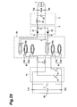
- Fig. 32 shows an arrangement of transformer 4 of the DC/DC converter shown in Fig. 10 .
- the primary coils are represented by 'P'
- the secondary coils are denoted 'S'
- the right windings are denoted by the subscript 'R'
- the left windings are denoted by the subscript 'L'.
- the secondary coils are single windings but are treated as left windings for the sake of convenience.
- the direction of winding from the outside to the inside of the coil as viewed from above Fig. 10 is the winding direction.
- the terminals which are directly connected to the anodes of the diodes 51 and 52 of the two terminals of the secondary coils are denoted 'D'.
- the direction in which the current flows in the coil as seen from the front of Fig. 10 is indicated by a dotted line arrow.
- the wiring which is connected to the innermost terminal of the coil is indicated by a segment that extends vertically from the center of each block and the wiring connected to the outside terminal is indicated by a segment that extends from the side of the blocks.
- a secondary coil S L , a primary coil P L , a primary coil P R , a secondary coil S L , a secondary coil S L , a primary coil P L , a primary coil P R , and a secondary coil S L are disposed in that order starting from the top along the path of the magnetic flux.
- the second and third primary coils P L and P R respectively can also be regarded as a single coil.
- the sixth and seventh primary coils P L and P R respectively can also be regarded as a single coil. The operation is as described earlier but will be described in simple terms.
- a current which flows in the opposite direction from the current flowing in the primary coil is to enter the secondary coil.
- the diode prevents the current supply and the current is therefore not supplied.
- the current which is to enter the secondary coil is supplied by the cathode of diodes 51 and 52, current flows in the secondary coil.
- the current which flows in the case of current path P1 is indicated by an arrow and a case where current does not flow is indicated by an the symbol x.
- the operation is the reverse of that of the case of current path P1.
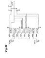
- Fig. 33 shows the arrangement of the transformer in a case where the placement of adjacent primary and secondary coils is switched.
- a primary coil P L , a secondary coil S L , a secondary coil S L , a primary coil P R , a primary coil P L , a secondary coil S L , a secondary coil S L , and a primary coil P R are disposed in that order starting from the top along the path of the magnetic flux.
- the connections are the same as those detailed above. Because the state of the magnetic coupling between adjacent coils does not change as a result of this position switching, the operation is the same as that described earlier.
- the above switching supply may output an AC signal by controlling the switching pulse signal applied to the inverter.
Landscapes
- Engineering & Computer Science (AREA)
- Power Engineering (AREA)
- Dc-Dc Converters (AREA)
- Coils Of Transformers For General Uses (AREA)
Applications Claiming Priority (1)
| Application Number | Priority Date | Filing Date | Title |
|---|---|---|---|
| JP2007094787A JP5034613B2 (ja) | 2007-03-30 | 2007-03-30 | Dc/dcコンバータ |
Publications (3)
| Publication Number | Publication Date |
|---|---|
| EP1976104A2 true EP1976104A2 (fr) | 2008-10-01 |
| EP1976104A3 EP1976104A3 (fr) | 2015-02-25 |
| EP1976104B1 EP1976104B1 (fr) | 2016-05-25 |
Family
ID=39616511
Family Applications (1)
| Application Number | Title | Priority Date | Filing Date |
|---|---|---|---|
| EP08005065.1A Active EP1976104B1 (fr) | 2007-03-30 | 2008-03-18 | Convertisseur de courant continu indirect avec un transformateur ayant des enroulements plans |
Country Status (3)
| Country | Link |
|---|---|
| US (1) | US8072305B2 (fr) |
| EP (1) | EP1976104B1 (fr) |
| JP (1) | JP5034613B2 (fr) |
Cited By (10)
| Publication number | Priority date | Publication date | Assignee | Title |
|---|---|---|---|---|
| EP2264882A1 (fr) * | 2009-06-19 | 2010-12-22 | TDK Corporation | Unité de commutation d'alimentation électrique |
| CN104836439A (zh) * | 2014-02-07 | 2015-08-12 | 株式会社丰田自动织机 | 变压器 |
| EP2230673A3 (fr) * | 2009-03-16 | 2015-10-28 | TDK Corporation | Transformator und Schaltnetzgerät |
| EP2918007A4 (fr) * | 2012-11-08 | 2017-04-12 | ABB Technology Ltd. | Convertisseur cc/cc, module d'entrée/sortie comprenant ledit convertisseur et procédé de commande de convertisseur cc/cc |
| CN107408449A (zh) * | 2015-03-16 | 2017-11-28 | 三菱电机株式会社 | 绝缘变压器 |
| EP2056439A3 (fr) * | 2007-10-30 | 2017-11-29 | TDK Corporation | Unité d'alimentation de puissance à commutation |
| CN109686540A (zh) * | 2017-10-19 | 2019-04-26 | 光寿科技有限公司 | 容抗性电压转换装置 |
| EP3477840A1 (fr) * | 2017-10-26 | 2019-05-01 | Univerza V Mariboru Fakulteta Za Elektrotehniko, Racunalnistvo In Informatiko | Transformateur de soudage |
| CN110463004A (zh) * | 2017-04-06 | 2019-11-15 | 三菱电机株式会社 | 功率转换装置 |
| CN110832766A (zh) * | 2017-07-04 | 2020-02-21 | 三菱电机株式会社 | 功率转换装置 |
Families Citing this family (38)
| Publication number | Priority date | Publication date | Assignee | Title |
|---|---|---|---|---|
| JP5047653B2 (ja) * | 2007-03-13 | 2012-10-10 | 三菱電機株式会社 | 半導体装置 |
| JP4978647B2 (ja) * | 2009-03-19 | 2012-07-18 | Tdk株式会社 | コイル部品、トランス及びスイッチング電源装置 |
| JP4821870B2 (ja) | 2009-03-19 | 2011-11-24 | Tdk株式会社 | コイル部品、トランス、スイッチング電源装置、及びコイル部品の製造方法 |
| JP5257204B2 (ja) | 2009-03-31 | 2013-08-07 | Tdk株式会社 | スイッチング電源装置 |
| JP5689587B2 (ja) * | 2009-03-31 | 2015-03-25 | 富士通株式会社 | 電力伝送装置 |
| US20110012435A1 (en) * | 2009-07-16 | 2011-01-20 | Fred Cohen | Center-tapped battery and power distribution system for same |
| CN102474187B (zh) * | 2009-07-23 | 2014-09-24 | 株式会社村田制作所 | 线圈一体型开关电源模块 |
| KR101121645B1 (ko) * | 2010-03-22 | 2012-02-28 | 삼성전기주식회사 | 평면형 트랜스포머 |
| JP5129294B2 (ja) * | 2010-04-28 | 2013-01-30 | 新東ホールディングス株式会社 | 電力変換装置 |
| GB2496163B (en) * | 2011-11-03 | 2015-11-11 | Enecsys Ltd | Transformer construction |
| DE102012003364A1 (de) * | 2012-02-22 | 2013-08-22 | Phoenix Contact Gmbh & Co. Kg | Planarer Übertrager |
| GB2501693B (en) * | 2012-05-01 | 2016-01-20 | Ge Aviat Systems Ltd | Apparatus and method for arc fault detection |
| JP6113045B2 (ja) * | 2013-10-08 | 2017-04-12 | 三菱電機株式会社 | 降圧トランスおよび絶縁型降圧コンバータ |
| CN103700473B (zh) * | 2013-12-12 | 2017-11-28 | 华为技术有限公司 | 耦合电感和功率变换器 |
| JP6227446B2 (ja) | 2014-03-12 | 2017-11-08 | 日立オートモティブシステムズ株式会社 | トランスおよびそれを用いた電力変換装置 |
| JP6384096B2 (ja) * | 2014-04-08 | 2018-09-05 | 株式会社デンソー | 電源装置 |
| US9305696B2 (en) * | 2014-07-08 | 2016-04-05 | Alliance Magnetics (H.K.) Co. Ltd. | Stacked inductor |
| JP6421484B2 (ja) * | 2014-07-28 | 2018-11-14 | Tdk株式会社 | コイル部品、コイル部品複合体およびトランス、ならびに電源装置 |
| WO2016076222A1 (fr) * | 2014-11-10 | 2016-05-19 | 三菱電機株式会社 | Convertisseur abaisseur de type isolant |
| US9672974B2 (en) | 2014-11-20 | 2017-06-06 | Panasonic Intellectual Property Management Co., Ltd. | Magnetic component and power transfer device |
| US10404178B2 (en) * | 2016-04-21 | 2019-09-03 | Mitsubishi Electric Corporation | Insulation type step-up converter |
| JP6238323B2 (ja) * | 2016-10-19 | 2017-11-29 | ルネサスエレクトロニクス株式会社 | 回路装置 |
| US20180197676A1 (en) * | 2017-01-10 | 2018-07-12 | General Electric Company | Insulation for tranformer or inductor |
| US12374487B2 (en) * | 2017-04-19 | 2025-07-29 | Narayan Powertech Pvt. Ltd. | Current transformer with current branches on primary conductor |
| JP6516910B1 (ja) * | 2018-07-06 | 2019-05-22 | 三菱電機株式会社 | 降圧コンバータ |
| CN115359999B (zh) | 2018-11-02 | 2026-04-10 | 台达电子企业管理(上海)有限公司 | 变压器模块及功率模块 |
| CN111145988B (zh) | 2018-11-02 | 2021-12-07 | 台达电子企业管理(上海)有限公司 | 变压器模块及功率模块 |
| US12002615B2 (en) | 2018-11-02 | 2024-06-04 | Delta Electronics (Shanghai) Co., Ltd. | Magnetic element, manufacturing method of magnetic element, and power module |
| US11133750B2 (en) * | 2018-11-02 | 2021-09-28 | Delta Electronics (Shanghai) Co., Ltd. | Power module |
| EP3648128B1 (fr) | 2018-11-02 | 2024-01-03 | Delta Electronics (Shanghai) Co., Ltd. | Module de transformateur et module de puissance |
| DE102018220415A1 (de) * | 2018-11-28 | 2020-05-28 | Zf Friedrichshafen Ag | Transformator, Gleichspannungswandler und elektrischer Kraftwagen |
| US11594361B1 (en) | 2018-12-18 | 2023-02-28 | Smart Wires Inc. | Transformer having passive cooling topology |
| US20200303114A1 (en) * | 2019-03-22 | 2020-09-24 | Cyntec Co., Ltd. | Inductor array in a single package |
| JP6991178B2 (ja) * | 2019-05-24 | 2022-01-12 | 株式会社Soken | 電力変換装置 |
| JP7314835B2 (ja) * | 2020-02-28 | 2023-07-26 | Tdk株式会社 | トランス、電力変換装置、および電力変換システム |
| JP7544544B2 (ja) * | 2020-09-16 | 2024-09-03 | 株式会社ダイヘン | プレーナ型変圧器 |
| CN114203414A (zh) * | 2020-09-17 | 2022-03-18 | 群光电能科技股份有限公司 | 变压器 |
| JP2022131545A (ja) * | 2021-02-26 | 2022-09-07 | ダイヤゼブラ電機株式会社 | 変圧器 |
Citations (1)
| Publication number | Priority date | Publication date | Assignee | Title |
|---|---|---|---|---|
| JP2629999B2 (ja) | 1990-02-01 | 1997-07-16 | 富士電機株式会社 | Dc/dcコンバータの直列接続回路 |
Family Cites Families (21)
| Publication number | Priority date | Publication date | Assignee | Title |
|---|---|---|---|---|
| US4613843A (en) * | 1984-10-22 | 1986-09-23 | Ford Motor Company | Planar coil magnetic transducer |
| US4613743A (en) * | 1984-12-03 | 1986-09-23 | General Electric Company | Arc welding adaptive process control system |
| FR2605453A1 (fr) * | 1986-10-15 | 1988-04-22 | Dassault Electronique | Transformateur haute frequence avec enroulement en circuit imprime, en particulier pour alimentation a tres haute tension |
| US4864486A (en) * | 1988-07-29 | 1989-09-05 | International Business Machines Corporation | Plank and frame transformer |
| JP3311391B2 (ja) * | 1991-09-13 | 2002-08-05 | ヴィエルティー コーポレーション | 漏洩インダクタンス低減トランス、これを用いた高周波回路及びパワーコンバータ並びにトランスにおける漏洩インダクタンスの低減方法 |
| US5168440A (en) * | 1991-10-02 | 1992-12-01 | International Business Machines Corporation | Transformer/rectifier assembly with a figure eight secondary structure |
| JPH06215951A (ja) * | 1993-01-19 | 1994-08-05 | Yokogawa Electric Corp | プリントコイル形トランス |
| JP3057203B2 (ja) * | 1993-04-19 | 2000-06-26 | 横河電機株式会社 | プリントコイル形トランス |
| JP3218585B2 (ja) * | 1993-11-18 | 2001-10-15 | 横河電機株式会社 | プリントコイル形トランス |
| JPH1041141A (ja) * | 1996-07-19 | 1998-02-13 | Tokin Corp | トランス |
| JP3509836B2 (ja) * | 1996-10-30 | 2004-03-22 | 横河電機株式会社 | プリントコイル形トランス |
| US5920473A (en) * | 1998-03-09 | 1999-07-06 | Magnetic Technology, Inc. | Dc-to-Dc power converter with integrated magnetic power transformer |
| US6026004A (en) * | 1998-12-21 | 2000-02-15 | Ruanduff Electrical Limited | Modular high voltage power supply with integral flux leakage compensation |
| JP2000260640A (ja) * | 1999-03-12 | 2000-09-22 | Cosel Co Ltd | 出力トランス |
| US20020163818A1 (en) * | 2001-03-05 | 2002-11-07 | Green Mark D. | Magnetic device and method of manufacture therefor |
| KR100420948B1 (ko) * | 2001-08-22 | 2004-03-02 | 한국전자통신연구원 | 병렬 분기 구조의 나선형 인덕터 |
| JP2004335780A (ja) * | 2003-05-08 | 2004-11-25 | Toyota Industries Corp | トランスの取付け構造 |
| JP2005033938A (ja) * | 2003-07-08 | 2005-02-03 | Sony Corp | 電源装置およびコンバータトランス |
| US7187263B2 (en) * | 2003-11-26 | 2007-03-06 | Vlt, Inc. | Printed circuit transformer |
| JP4284656B2 (ja) * | 2004-06-25 | 2009-06-24 | Tdkラムダ株式会社 | トランス構造 |
| JP4319613B2 (ja) * | 2004-11-22 | 2009-08-26 | 株式会社デンソー | 車両用dc−dcコンバータ装置 |
-
2007
- 2007-03-30 JP JP2007094787A patent/JP5034613B2/ja active Active
-
2008
- 2008-03-13 US US12/047,770 patent/US8072305B2/en active Active
- 2008-03-18 EP EP08005065.1A patent/EP1976104B1/fr active Active
Patent Citations (1)
| Publication number | Priority date | Publication date | Assignee | Title |
|---|---|---|---|---|
| JP2629999B2 (ja) | 1990-02-01 | 1997-07-16 | 富士電機株式会社 | Dc/dcコンバータの直列接続回路 |
Cited By (17)
| Publication number | Priority date | Publication date | Assignee | Title |
|---|---|---|---|---|
| EP2056439A3 (fr) * | 2007-10-30 | 2017-11-29 | TDK Corporation | Unité d'alimentation de puissance à commutation |
| EP2230673A3 (fr) * | 2009-03-16 | 2015-10-28 | TDK Corporation | Transformator und Schaltnetzgerät |
| US8339808B2 (en) | 2009-06-19 | 2012-12-25 | Tdk Corporation | Switching power supply unit |
| EP2264882A1 (fr) * | 2009-06-19 | 2010-12-22 | TDK Corporation | Unité de commutation d'alimentation électrique |
| EP2918007A4 (fr) * | 2012-11-08 | 2017-04-12 | ABB Technology Ltd. | Convertisseur cc/cc, module d'entrée/sortie comprenant ledit convertisseur et procédé de commande de convertisseur cc/cc |
| CN104836439A (zh) * | 2014-02-07 | 2015-08-12 | 株式会社丰田自动织机 | 变压器 |
| CN107408449A (zh) * | 2015-03-16 | 2017-11-28 | 三菱电机株式会社 | 绝缘变压器 |
| CN107408449B (zh) * | 2015-03-16 | 2019-03-05 | 三菱电机株式会社 | 绝缘变压器 |
| CN110463004A (zh) * | 2017-04-06 | 2019-11-15 | 三菱电机株式会社 | 功率转换装置 |
| CN110832766A (zh) * | 2017-07-04 | 2020-02-21 | 三菱电机株式会社 | 功率转换装置 |
| EP3651340A4 (fr) * | 2017-07-04 | 2020-07-15 | Mitsubishi Electric Corporation | Dispositif de conversion de puissance |
| US11128226B2 (en) | 2017-07-04 | 2021-09-21 | Mitsubishi Electric Corporation | Power conversion device |
| CN110832766B (zh) * | 2017-07-04 | 2022-03-01 | 三菱电机株式会社 | 功率转换装置 |
| EP3483903A3 (fr) * | 2017-10-19 | 2019-07-17 | AMTB Technology | Transformateur de tension à réactance capacitive |
| CN109686540A (zh) * | 2017-10-19 | 2019-04-26 | 光寿科技有限公司 | 容抗性电压转换装置 |
| CN109686540B (zh) * | 2017-10-19 | 2021-06-18 | 光寿科技有限公司 | 容抗性电压转换装置 |
| EP3477840A1 (fr) * | 2017-10-26 | 2019-05-01 | Univerza V Mariboru Fakulteta Za Elektrotehniko, Racunalnistvo In Informatiko | Transformateur de soudage |
Also Published As
| Publication number | Publication date |
|---|---|
| EP1976104A3 (fr) | 2015-02-25 |
| JP5034613B2 (ja) | 2012-09-26 |
| US20080239759A1 (en) | 2008-10-02 |
| US8072305B2 (en) | 2011-12-06 |
| JP2008253113A (ja) | 2008-10-16 |
| EP1976104B1 (fr) | 2016-05-25 |
Similar Documents
| Publication | Publication Date | Title |
|---|---|---|
| EP1976104B1 (fr) | Convertisseur de courant continu indirect avec un transformateur ayant des enroulements plans | |
| US11121633B2 (en) | Low common mode noise transformers and switch-mode DC-DC power converters | |
| EP1770849A2 (fr) | Unité d'alimentation de puissance à découpage | |
| US10886046B2 (en) | Integrated magnetic component and switched mode power converter | |
| EP1981158B1 (fr) | Convertisseur de courant continu indirect avec des transformateurs parallèles ayant des enroulements plans | |
| EP1760867B1 (fr) | Unité d'alimentation de puissance à découpage | |
| US9148064B2 (en) | Multi-phase switching power conversion circuit | |
| US6281779B1 (en) | Coil device and switching power supply apparatus using the same | |
| US7209024B2 (en) | Filter circuit and power supply unit | |
| TW202213402A (zh) | 平板繞組變壓器 | |
| JP2009142088A (ja) | 表示装置用dc−dcコンバータ | |
| US20240363283A1 (en) | Power module and power circuit | |
| US7362206B1 (en) | Variable transformer | |
| CN113168956B (zh) | 低高度耦合电感器 | |
| US10164542B2 (en) | Electronic converter, and corresponding method for designing a magnetic component | |
| JP2023504037A (ja) | セグメント化された巻線を有する電力変換器 | |
| JP2000173837A (ja) | スイッチング電源用のシートトランス | |
| US20250246365A1 (en) | Half-turn winding transformer, circuit topology and power device | |
| CN223884247U (zh) | 集成平面变压器、功率变换器、电源模块和储能设备 | |
| US20240275294A1 (en) | Magnetic apparatus with symmetric quadruple or octuple winding arrangement, power module, power conversion device, and dc-dc conversion device | |
| WO2025111799A1 (fr) | Circuit de redressement, circuit de régulation de tension, transformateur, ensemble carte de circuit imprimé et serveur |
Legal Events
| Date | Code | Title | Description |
|---|---|---|---|
| PUAI | Public reference made under article 153(3) epc to a published international application that has entered the european phase |
Free format text: ORIGINAL CODE: 0009012 |
|
| AK | Designated contracting states |
Kind code of ref document: A2 Designated state(s): AT BE BG CH CY CZ DE DK EE ES FI FR GB GR HR HU IE IS IT LI LT LU LV MC MT NL NO PL PT RO SE SI SK TR |
|
| AX | Request for extension of the european patent |
Extension state: AL BA MK RS |
|
| RAP1 | Party data changed (applicant data changed or rights of an application transferred) |
Owner name: TDK CORPORATION |
|
| RAP1 | Party data changed (applicant data changed or rights of an application transferred) |
Owner name: TDK CORPORATION |
|
| PUAL | Search report despatched |
Free format text: ORIGINAL CODE: 0009013 |
|
| AK | Designated contracting states |
Kind code of ref document: A3 Designated state(s): AT BE BG CH CY CZ DE DK EE ES FI FR GB GR HR HU IE IS IT LI LT LU LV MC MT NL NO PL PT RO SE SI SK TR |
|
| AX | Request for extension of the european patent |
Extension state: AL BA MK RS |
|
| RIC1 | Information provided on ipc code assigned before grant |
Ipc: H01F 27/34 20060101ALN20150119BHEP Ipc: H01F 27/28 20060101ALN20150119BHEP Ipc: H02M 3/337 20060101AFI20150119BHEP Ipc: H02M 7/00 20060101ALI20150119BHEP |
|
| 17P | Request for examination filed |
Effective date: 20150810 |
|
| RBV | Designated contracting states (corrected) |
Designated state(s): AT BE BG CH CY CZ DE DK EE ES FI FR GB GR HR HU IE IS IT LI LT LU LV MC MT NL NO PL PT RO SE SI SK TR |
|
| AKX | Designation fees paid |
Designated state(s): AT BE BG CH CY CZ DE DK EE ES FI FR GB GR HR HU IE IS IT LI LT LU LV MC MT NL NO PL PT RO SE SI SK TR |
|
| AXX | Extension fees paid |
Extension state: BA Extension state: RS Extension state: AL Extension state: MK |
|
| RIC1 | Information provided on ipc code assigned before grant |
Ipc: H01F 27/34 20060101ALN20151110BHEP Ipc: H02M 7/00 20060101ALI20151110BHEP Ipc: H02M 3/337 20060101AFI20151110BHEP Ipc: H01F 27/28 20060101ALN20151110BHEP |
|
| GRAP | Despatch of communication of intention to grant a patent |
Free format text: ORIGINAL CODE: EPIDOSNIGR1 |
|
| INTG | Intention to grant announced |
Effective date: 20151221 |
|
| GRAS | Grant fee paid |
Free format text: ORIGINAL CODE: EPIDOSNIGR3 |
|
| GRAA | (expected) grant |
Free format text: ORIGINAL CODE: 0009210 |
|
| AK | Designated contracting states |
Kind code of ref document: B1 Designated state(s): AT BE BG CH CY CZ DE DK EE ES FI FR GB GR HR HU IE IS IT LI LT LU LV MC MT NL NO PL PT RO SE SI SK TR |
|
| REG | Reference to a national code |
Ref country code: GB Ref legal event code: FG4D |
|
| REG | Reference to a national code |
Ref country code: CH Ref legal event code: EP |
|
| REG | Reference to a national code |
Ref country code: IE Ref legal event code: FG4D Ref country code: AT Ref legal event code: REF Ref document number: 803053 Country of ref document: AT Kind code of ref document: T Effective date: 20160615 |
|
| REG | Reference to a national code |
Ref country code: DE Ref legal event code: R096 Ref document number: 602008044381 Country of ref document: DE |
|
| REG | Reference to a national code |
Ref country code: LT Ref legal event code: MG4D |
|
| REG | Reference to a national code |
Ref country code: NL Ref legal event code: MP Effective date: 20160525 |
|
| PG25 | Lapsed in a contracting state [announced via postgrant information from national office to epo] |
Ref country code: NL Free format text: LAPSE BECAUSE OF FAILURE TO SUBMIT A TRANSLATION OF THE DESCRIPTION OR TO PAY THE FEE WITHIN THE PRESCRIBED TIME-LIMIT Effective date: 20160525 Ref country code: NO Free format text: LAPSE BECAUSE OF FAILURE TO SUBMIT A TRANSLATION OF THE DESCRIPTION OR TO PAY THE FEE WITHIN THE PRESCRIBED TIME-LIMIT Effective date: 20160825 Ref country code: FI Free format text: LAPSE BECAUSE OF FAILURE TO SUBMIT A TRANSLATION OF THE DESCRIPTION OR TO PAY THE FEE WITHIN THE PRESCRIBED TIME-LIMIT Effective date: 20160525 Ref country code: LT Free format text: LAPSE BECAUSE OF FAILURE TO SUBMIT A TRANSLATION OF THE DESCRIPTION OR TO PAY THE FEE WITHIN THE PRESCRIBED TIME-LIMIT Effective date: 20160525 |
|
| REG | Reference to a national code |
Ref country code: AT Ref legal event code: MK05 Ref document number: 803053 Country of ref document: AT Kind code of ref document: T Effective date: 20160525 |
|
| PG25 | Lapsed in a contracting state [announced via postgrant information from national office to epo] |
Ref country code: SE Free format text: LAPSE BECAUSE OF FAILURE TO SUBMIT A TRANSLATION OF THE DESCRIPTION OR TO PAY THE FEE WITHIN THE PRESCRIBED TIME-LIMIT Effective date: 20160525 Ref country code: ES Free format text: LAPSE BECAUSE OF FAILURE TO SUBMIT A TRANSLATION OF THE DESCRIPTION OR TO PAY THE FEE WITHIN THE PRESCRIBED TIME-LIMIT Effective date: 20160525 Ref country code: LV Free format text: LAPSE BECAUSE OF FAILURE TO SUBMIT A TRANSLATION OF THE DESCRIPTION OR TO PAY THE FEE WITHIN THE PRESCRIBED TIME-LIMIT Effective date: 20160525 Ref country code: GR Free format text: LAPSE BECAUSE OF FAILURE TO SUBMIT A TRANSLATION OF THE DESCRIPTION OR TO PAY THE FEE WITHIN THE PRESCRIBED TIME-LIMIT Effective date: 20160826 Ref country code: PT Free format text: LAPSE BECAUSE OF FAILURE TO SUBMIT A TRANSLATION OF THE DESCRIPTION OR TO PAY THE FEE WITHIN THE PRESCRIBED TIME-LIMIT Effective date: 20160926 Ref country code: HR Free format text: LAPSE BECAUSE OF FAILURE TO SUBMIT A TRANSLATION OF THE DESCRIPTION OR TO PAY THE FEE WITHIN THE PRESCRIBED TIME-LIMIT Effective date: 20160525 |
|
| PG25 | Lapsed in a contracting state [announced via postgrant information from national office to epo] |
Ref country code: IT Free format text: LAPSE BECAUSE OF FAILURE TO SUBMIT A TRANSLATION OF THE DESCRIPTION OR TO PAY THE FEE WITHIN THE PRESCRIBED TIME-LIMIT Effective date: 20160525 |
|
| PG25 | Lapsed in a contracting state [announced via postgrant information from national office to epo] |
Ref country code: RO Free format text: LAPSE BECAUSE OF FAILURE TO SUBMIT A TRANSLATION OF THE DESCRIPTION OR TO PAY THE FEE WITHIN THE PRESCRIBED TIME-LIMIT Effective date: 20160525 Ref country code: SK Free format text: LAPSE BECAUSE OF FAILURE TO SUBMIT A TRANSLATION OF THE DESCRIPTION OR TO PAY THE FEE WITHIN THE PRESCRIBED TIME-LIMIT Effective date: 20160525 Ref country code: DK Free format text: LAPSE BECAUSE OF FAILURE TO SUBMIT A TRANSLATION OF THE DESCRIPTION OR TO PAY THE FEE WITHIN THE PRESCRIBED TIME-LIMIT Effective date: 20160525 Ref country code: CZ Free format text: LAPSE BECAUSE OF FAILURE TO SUBMIT A TRANSLATION OF THE DESCRIPTION OR TO PAY THE FEE WITHIN THE PRESCRIBED TIME-LIMIT Effective date: 20160525 Ref country code: EE Free format text: LAPSE BECAUSE OF FAILURE TO SUBMIT A TRANSLATION OF THE DESCRIPTION OR TO PAY THE FEE WITHIN THE PRESCRIBED TIME-LIMIT Effective date: 20160525 |
|
| PG25 | Lapsed in a contracting state [announced via postgrant information from national office to epo] |
Ref country code: BE Free format text: LAPSE BECAUSE OF FAILURE TO SUBMIT A TRANSLATION OF THE DESCRIPTION OR TO PAY THE FEE WITHIN THE PRESCRIBED TIME-LIMIT Effective date: 20160525 Ref country code: AT Free format text: LAPSE BECAUSE OF FAILURE TO SUBMIT A TRANSLATION OF THE DESCRIPTION OR TO PAY THE FEE WITHIN THE PRESCRIBED TIME-LIMIT Effective date: 20160525 Ref country code: PL Free format text: LAPSE BECAUSE OF FAILURE TO SUBMIT A TRANSLATION OF THE DESCRIPTION OR TO PAY THE FEE WITHIN THE PRESCRIBED TIME-LIMIT Effective date: 20160525 |
|
| REG | Reference to a national code |
Ref country code: DE Ref legal event code: R097 Ref document number: 602008044381 Country of ref document: DE |
|
| PLBE | No opposition filed within time limit |
Free format text: ORIGINAL CODE: 0009261 |
|
| STAA | Information on the status of an ep patent application or granted ep patent |
Free format text: STATUS: NO OPPOSITION FILED WITHIN TIME LIMIT |
|
| 26N | No opposition filed |
Effective date: 20170228 |
|
| PG25 | Lapsed in a contracting state [announced via postgrant information from national office to epo] |
Ref country code: SI Free format text: LAPSE BECAUSE OF FAILURE TO SUBMIT A TRANSLATION OF THE DESCRIPTION OR TO PAY THE FEE WITHIN THE PRESCRIBED TIME-LIMIT Effective date: 20160525 |
|
| REG | Reference to a national code |
Ref country code: CH Ref legal event code: PL |
|
| GBPC | Gb: european patent ceased through non-payment of renewal fee |
Effective date: 20170318 |
|
| PG25 | Lapsed in a contracting state [announced via postgrant information from national office to epo] |
Ref country code: MC Free format text: LAPSE BECAUSE OF FAILURE TO SUBMIT A TRANSLATION OF THE DESCRIPTION OR TO PAY THE FEE WITHIN THE PRESCRIBED TIME-LIMIT Effective date: 20160525 |
|
| REG | Reference to a national code |
Ref country code: IE Ref legal event code: MM4A |
|
| REG | Reference to a national code |
Ref country code: FR Ref legal event code: ST Effective date: 20171130 |
|
| PG25 | Lapsed in a contracting state [announced via postgrant information from national office to epo] |
Ref country code: LU Free format text: LAPSE BECAUSE OF NON-PAYMENT OF DUE FEES Effective date: 20170318 Ref country code: FR Free format text: LAPSE BECAUSE OF NON-PAYMENT OF DUE FEES Effective date: 20170331 |
|
| PG25 | Lapsed in a contracting state [announced via postgrant information from national office to epo] |
Ref country code: CH Free format text: LAPSE BECAUSE OF NON-PAYMENT OF DUE FEES Effective date: 20170331 Ref country code: LI Free format text: LAPSE BECAUSE OF NON-PAYMENT OF DUE FEES Effective date: 20170331 Ref country code: IE Free format text: LAPSE BECAUSE OF NON-PAYMENT OF DUE FEES Effective date: 20170318 Ref country code: GB Free format text: LAPSE BECAUSE OF NON-PAYMENT OF DUE FEES Effective date: 20170318 |
|
| PG25 | Lapsed in a contracting state [announced via postgrant information from national office to epo] |
Ref country code: MT Free format text: LAPSE BECAUSE OF NON-PAYMENT OF DUE FEES Effective date: 20170318 |
|
| PG25 | Lapsed in a contracting state [announced via postgrant information from national office to epo] |
Ref country code: HU Free format text: LAPSE BECAUSE OF FAILURE TO SUBMIT A TRANSLATION OF THE DESCRIPTION OR TO PAY THE FEE WITHIN THE PRESCRIBED TIME-LIMIT; INVALID AB INITIO Effective date: 20080318 |
|
| PG25 | Lapsed in a contracting state [announced via postgrant information from national office to epo] |
Ref country code: BG Free format text: LAPSE BECAUSE OF FAILURE TO SUBMIT A TRANSLATION OF THE DESCRIPTION OR TO PAY THE FEE WITHIN THE PRESCRIBED TIME-LIMIT Effective date: 20160525 |
|
| PG25 | Lapsed in a contracting state [announced via postgrant information from national office to epo] |
Ref country code: CY Free format text: LAPSE BECAUSE OF NON-PAYMENT OF DUE FEES Effective date: 20160525 |
|
| PG25 | Lapsed in a contracting state [announced via postgrant information from national office to epo] |
Ref country code: TR Free format text: LAPSE BECAUSE OF FAILURE TO SUBMIT A TRANSLATION OF THE DESCRIPTION OR TO PAY THE FEE WITHIN THE PRESCRIBED TIME-LIMIT Effective date: 20160525 |
|
| PG25 | Lapsed in a contracting state [announced via postgrant information from national office to epo] |
Ref country code: IS Free format text: LAPSE BECAUSE OF FAILURE TO SUBMIT A TRANSLATION OF THE DESCRIPTION OR TO PAY THE FEE WITHIN THE PRESCRIBED TIME-LIMIT Effective date: 20160925 |
|
| PGFP | Annual fee paid to national office [announced via postgrant information from national office to epo] |
Ref country code: DE Payment date: 20250128 Year of fee payment: 18 |