EP1977991A2 - Composants microstructurés dotés d'un substrat et d'une puce mise en contact direct avec le substrat, et son procédé de fabrication - Google Patents
Composants microstructurés dotés d'un substrat et d'une puce mise en contact direct avec le substrat, et son procédé de fabrication Download PDFInfo
- Publication number
- EP1977991A2 EP1977991A2 EP20080154171 EP08154171A EP1977991A2 EP 1977991 A2 EP1977991 A2 EP 1977991A2 EP 20080154171 EP20080154171 EP 20080154171 EP 08154171 A EP08154171 A EP 08154171A EP 1977991 A2 EP1977991 A2 EP 1977991A2
- Authority
- EP
- European Patent Office
- Prior art keywords
- chip
- substrate
- oder
- component according
- der
- Prior art date
- Legal status (The legal status is an assumption and is not a legal conclusion. Google has not performed a legal analysis and makes no representation as to the accuracy of the status listed.)
- Ceased
Links
Images

Classifications
-
- B—PERFORMING OPERATIONS; TRANSPORTING
- B81—MICROSTRUCTURAL TECHNOLOGY
- B81C—PROCESSES OR APPARATUS SPECIALLY ADAPTED FOR THE MANUFACTURE OR TREATMENT OF MICROSTRUCTURAL DEVICES OR SYSTEMS
- B81C1/00—Manufacture or treatment of devices or systems in or on a substrate
- B81C1/00015—Manufacture or treatment of devices or systems in or on a substrate for manufacturing microsystems
- B81C1/00222—Integrating an electronic processing unit with a micromechanical structure
- B81C1/0023—Packaging together an electronic processing unit die and a micromechanical structure die
-
- B—PERFORMING OPERATIONS; TRANSPORTING
- B81—MICROSTRUCTURAL TECHNOLOGY
- B81B—MICROSTRUCTURAL DEVICES OR SYSTEMS, e.g. MICROMECHANICAL DEVICES
- B81B2207/00—Microstructural systems or auxiliary parts thereof
- B81B2207/01—Microstructural systems or auxiliary parts thereof comprising a micromechanical device connected to control or processing electronics, i.e. Smart-MEMS
- B81B2207/012—Microstructural systems or auxiliary parts thereof comprising a micromechanical device connected to control or processing electronics, i.e. Smart-MEMS the micromechanical device and the control or processing electronics being separate parts in the same package
-
- H—ELECTRICITY
- H10—SEMICONDUCTOR DEVICES; ELECTRIC SOLID-STATE DEVICES NOT OTHERWISE PROVIDED FOR
- H10W—GENERIC PACKAGES, INTERCONNECTIONS, CONNECTORS OR OTHER CONSTRUCTIONAL DETAILS OF DEVICES COVERED BY CLASS H10
- H10W90/00—Package configurations
- H10W90/701—Package configurations characterised by the relative positions of pads or connectors relative to package parts
- H10W90/721—Package configurations characterised by the relative positions of pads or connectors relative to package parts of bump connectors
- H10W90/724—Package configurations characterised by the relative positions of pads or connectors relative to package parts of bump connectors between a chip and a stacked insulating package substrate, interposer or RDL
Definitions
- the present invention is directed to the fabrication of microstructured devices (largely in the form of subsystems) that are useful in the formation of micro devices such as microsensors (pressure sensors, inertial sensors, MEMS and the like), microphones or optical detectors.
- These components or subsystems comprise a substrate, for example a silicon wafer with evaluation circuit (ASIC), which is often to be subdivided later into a plurality of substrates for a plurality of such microcomponents, as well as at least one chip, which generally carries a plurality of active structures, upside down the active structures down, applied to the substrate and connected to this mechanically and electrically / electronically.
- ASIC silicon wafer with evaluation circuit
- chips may in turn contain components e.g. a single chip wafer.
- the invention relates to such components or subsystems in which both the surface of the substrate and the surface of the chip (without conductor structures and without active structures seen) is flat or substantially planar.
- microsystem components are preferably manufactured using semiconductor technology manufacturing methods. As a result, many components can be produced at the same time cost. These components are, however, due to their very small dimensions, extremely sensitive and must be protected during operation or even during production against external influences. This is accomplished by hermetically sealing these components with protective caps.
- Capping methods have been known for some time. It is often used in this case that separate cover chips (lid wafers) are adhesively bonded to the wafers containing the active structures or applied by other joining methods and thus the elements are hermetically sealed. Also known for some time, methods (ystem technic wafer M icro S) encapsulate an MST wafer at the wafer level.
- a wafer which may consist for example of glass or silicon and generally contains one or more cavities for receiving the active component parts, connected by means of an anodic connection or by using glass solders. Less widespread in wafer joining technology is the use of metallic or metal-containing solders.
- MEMS packaging This technique is also generally proposed for "MEMS packaging", because it could provide sealing connections, such as e.g. may be necessary for working in vacuum or under certain gas / gas microsensors microsensors and because the components do not necessarily have to be the same size.
- sealing connections such as e.g. may be necessary for working in vacuum or under certain gas / gas microsensors microsensors and because the components do not necessarily have to be the same size.
- packaging a microsensor or other active structure From the article, therefore, a person skilled in the art can not gather information on how the electrical connections between the components could run in such an arrangement.
- the assembly and connection technology for microsensory and other active microcomponents must deal with the following problems: Between the sensor elements and an electronic evaluation circuit (eg circuits for controlling the sensor element (s), measuring their signals and communicating with external sensors electrical circuits) electrical connections must be created. Furthermore, the often extremely sensitive microsensitive components and / or the semiconductor circuit must be protected from harmful environmental influences such as excessive mechanical stress, interfering electromagnetic radiation and unwanted particles. Also, the protection against liquids, gases or elementary particles may be required. Finally, the active system, ie the active component such as sensor / actuator or a combination of such components, must be integrated into a target system, eg a printed circuit board, a housing or a surface, exposed to environmental influences is.
- a target system eg a printed circuit board, a housing or a surface
- Environmental influences can be either disruptive (eg, the above-described influences or unsuitable gas pressure, undesired gas composition), and therefore they must be prevented, or they can be useful (eg, a motion change or temperature to be detected), leaving the latter undisturbed inside the device should be detectable.
- a suitable medium for example, liquid or an optical lens
- the integration is facilitated, for example, by the installation space, the height or the required footprint be reduced.
- the object of the present invention is to provide a compact microstructured component or subsystem comprising packaged, active microstructures such as microsensors (eg inertial sensors for velocity, acceleration, rotation or sensors for humidity, light, temperature, radioactivity or the like) and / or microactuators and the like .ae. contains and is a micro device or can be singulated to such devices, the structure of the structure of this component or subsystem helps to reduce the overall cost of manufacturing the micro devices by making it possible with simpler measures than previously required for comparable structures.
- active microstructures such as microsensors (eg inertial sensors for velocity, acceleration, rotation or sensors for humidity, light, temperature, radioactivity or the like) and / or microactuators and the like .ae. contains and is a micro device or can be singulated to such devices, the structure of the structure of this component or subsystem helps to reduce the overall cost of manufacturing the micro devices by making it possible with simpler measures than previously required for comparable structures.
- a microstructured component for microsensors or other active microcomponents comprising a substrate and at least one chip, which carries on its surface facing the substrate one or more active structures, wherein the substrate and the at least one chip via a sealing frame are interconnected such that the one or more active structure (s) are sufficiently protected from environmental influences, each chip carrying on its surface facing the substrate at least one electrical contact point associated with one or more active ones Structure (s) is in conductive contact, and that the or at least one of said electrical contact points of each chip is electrically connected to an on the substrate, electrical contact point, which in turn is connected to a conductor pattern on or within the substrate, which can be contacted on the substrate outside the areas occupied by the chip (s).
- the microstructured components of the present invention may in suitable cases of a (single) substrate, such as an already isolated ASIC or a such wafer fragment, and a (single) chip composed.
- a substrate for example a wafer with a diameter of 20-30 cm
- Such systems are also referred to below as subsystems. They can be separated later in a known manner, for example by wafer saws, to produce the individual microcomponents.
- any substrate which can be used for microcomponents or subsystems is suitable as the substrate in the present invention.
- the substrate may be a printed circuit board, a glass substrate or the like.
- the basic task of the substrate is to ensure at least one contact point for the interconnection of the later microcomponent with the respectively required external components for the forwarding of the signals received from the active structure (sensors, actuators) of each chip, from which the corresponding electrical components Data can be tapped.
- the substrate itself may also comprise suitable circuitry, e.g. an electronic evaluation circuit, comprising circuits for controlling the sensor element, for measuring their signals and / or for communication with external electrical circuits. This facilitates the unbundling of a large number of signals in many cases by performing electronic preprocessing within the subsystem.
- a substrate is any one on which a chip or a plurality of chips or a chip wafer is to be set, in order to combine an electrical rewiring and a protective capping with one another (eg arranging (if necessary rotatable) image sensors or mirror elements a chip for protection against environmental influences, and combining this chip with a translucent substrate, possibly with a technology required redistribution of the contact points over a larger area, so that the beam path from an external light source, such as a laser, to the image sensor or the mirror unhindered is).
- an external light source such as a laser
- the surface of the substrate facing the chips may be substantially planar, thereby reducing costs otherwise required Surface structuring can be avoided.
- the conductor structures can be applied superficially; but they are preferably buried.
- the substrate is a silicon wafer, several hundred chips can be arranged thereon. These may be the same or different.
- Each chip or each chip element of a chip wafer has one or more active structures in accordance with the use of the future microcomponent.
- active structure in the context of the present invention is intended to include structures that can detect and convert environmental influences such as speeds, accelerations, rotations, light radiation, moisture, magnetic field, sound waves, pH, temperature or the like into electrical signals (hereinafter referred to as Sensors referred to), the electrical, electromagnetic, mechanical or thermal energy record, convert, store and / or can give off (eg batteries, accumulators) and / or can perform the movements (“actuators”), but not limited thereto.
- components provided for airbags may contain three different acceleration sensors which can detect accelerations in the three spatial directions x, y, z.
- a chip may contain different active structures with different tasks, for example different sensors and / or batteries that require different environmental conditions for their operation.
- the active structure (s) may be mounted on the surface of the chip or the chip wafer, for which reason it is not necessary to provide cavities in the chip surface for this purpose. This can therefore be designed essentially flat.
- the chip surface may also have recesses if this is necessary or desirable, for example, in the case where the active structure (s) are relatively high and / or because the active structure (s) is derived from the Chip surface were etched out.
- a sealing frame connects the chip (s) to the substrate. This defines the distance between the substrate and the chip surface (s). It is therefore chosen so high that the active structures can be housed safely and without knocking.
- the sealing frame ensures the mechanical connection between the chip and wafer surface. It can be made of any material which has the necessary rigidity, for example of an organic one Polymer material such as polyimide or Benzocyclobuten (BCB) or an inorganic material such as a metal or alloy or glass or glass frit. Suitable metals are Au, Pd, Al or alloys such as those of Cu / Sn or Cu / Au.
- the frame may be made of a single material or may be formed by joining different metals deposited on the substrate and the chip component, respectively, which alloy in the connection region. It may be applied to a substrate of adhesion promoter and / or a nucleating metal.
- sealing frame is not necessarily to be understood to mean that it is completely continuous or completely sealing / hermetic.
- the sealing frame may instead be broken if the active structures can / must operate in ambient conditions. If necessary, it can be subdivided so that it encloses several spaces, so that different active structures can be separated from one another. This can e.g. be necessary if their environment should have different pressures / gas mixtures. If, in a defined gas atmosphere, these cavities are separated from the ambient atmosphere by the bonding of the substrate and the chip, the gas pressure or the gas mixture in one or more of these spaces can be e.g.
- getter material which absorbs gas molecules when activated in a definable manner and thus changes the gas atmosphere.
- Getter material can also be used to absorb moisture or even trap particles. This getter material is preferably provided on the substrate surface for geometrical reasons.
- the sealing frame may also be configured to encase only a portion of the on-chip active structures while exposing at least one of these active structures to the ambient atmosphere or medium in which the active device is to operate. This can be favorable, for example, if the microcomponent to be produced is to have a moisture sensor.
- the sealing frame may be configured to allow limited or controlled gas delivery for that structure (s). For example, it may each comprise from outside to inside continuous layers of palladium (permeable to hydrogen), SiO 2 (permeable to helium) or of carbon nanotubes, the latter material being water vapor permeable.
- the sealing frame has a special geometric shape, for example a fluid channel.
- a fluid channel for this purpose, it can be formed, for example, at the required locations as a double channel, into which liquid can flow in or out through two substrate perforations.
- the structure of the subsystem has the following advantages with regard to the signal routing: Conductor lengths can be kept very short, so that good or even better (because more constant) electrical properties are achieved in spite of low area use than in conventional construction methods. Likewise, the preferred combination with a semiconductor circuit (referred to in the art as a "system-in-package") allows only the signals needed in the application circuitry to be routed out of the measurement system and internally supply the sensor supply and signal transfer, thereby achieving higher reliability of the system ,
- the mechanical connection between chip (s) and substrate ie the sealing frame
- the materials for the sealing frame and the contacts may be the same. In these cases, but not necessarily, the construction of the material for the sealing rings and the contacts can take place together, which saves work steps and costs.
- both the chip (s) and the substrate are treated in a suitable manner.
- the steps may include electrodeposition or electroless deposition of metals.
- the substrate or wafer and / or chip surfaces can be provided in a first step with a continuous metal layer (potential layer), for example optionally with titanium as a primer (acts as adhesion promoter) and a layer deposited thereon from one or more suitable metals such as Cr, Ti, Cr / Cu, Ti / Cu or TiN.
- This layer is applied in a suitable thickness, for example with 3-50 nm, preferably about 5-20 nm and particularly preferably about 10 nm.
- a gold layer which has a thickness of up to about 200 nm, preferably up to about 100 nm, may additionally be deposited as the uppermost layer.
- the metal is overcoated with a photoresist, which is then patterned using a suitable mask.
- the exposed areas are then provided with the actual metal layer, e.g. can be made of gold, copper, nickel or possibly also palladium or a combination of these materials.
- the gold layer may possibly still be overlaid with a tin layer.
- the potential layer is energized.
- the metal layer is grown in sufficient total thickness (thickness on the substrate plus thickness on the chip) to allow the active structure (s) on the chips to find enough space between the substrate and the chip surface after bonding.
- the total thickness may be, for example, about 0.5 ⁇ m to 50 ⁇ m, preferably 2-20 ⁇ m, depending on the structures on the chips. If an additional Sn layer is to be present, a thickness proportion of approximately 1-3 ⁇ m suffices for this.
- the paint preferably by means of suitable solvents
- the metal primer e.g., dry, by argon bombardment, or in a wet etching process, which etches away the very thin starting metallization
- Gold, nickel, copper, possibly palladium or the combination thereof described above is preferably used as the uppermost layer, if the construction of the contacts and the sealing frame is to take place only on one side, the chip side or the substrate side. Because these metals can react with the opposite surface during subsequent pressing. If this, which is preferred, consists of silicon, this forms namely an intimate connection of a metal-silicon alloy, which melts relatively high. In such embodiments, Si protrusions or rings can be formed on the chip surface, which are realized for example by means of etching.
- a structure with a gold layer is realized on both sides.
- substrate and / or chip side can still be applied to the above-mentioned thin tin layer.
- an Au / Sn alloy can form between the parts, which melts higher than the pure metals. This technique is also referred to as reactive joining ("soldering").
- the sealing ring and the contact structures are instead made of different materials and / or by means of different techniques. They can each consist of metal.
- the sealing ring may instead consist of an organic material, for example polyimide or Benzocyclobutene (BCB). This material is applied on one or both sides (chip and / or substrate side) in the form of prepolymers or monomers surface and exposed through a suitable mask. After dissolution of the unexposed material, the structured sealing ring is obtained.
- sealing ring may be formed only on the substrate because the chip surfaces carry active structures that would need to be protected during manufacture.
- aluminum structures can be sputtered or vapor-deposited.
- These bumps allow the distance between the substrate surface and the sensor surface to be set very precisely.
- the bumps or other raised contact points can advantageously be used equally as structures for the adjustment between the substrate and the chip / chip wafer or the individual chips. For this, they or some of them are set up slightly higher (eg, about 0.5-5 ⁇ m higher) than the sealing frame.
- the connection of the substrate to the chip (s) preferably takes place in two stages in these cases. In the first stage, the parts are moved relative to each other in the correct horizontal position and prefixed to store this position. For this purpose, 1 to 3 breakpoints per chip are sufficient; Cheap are about up to 4 breakpoints.
- the sealing frame must not seal in this phase, it is desirable that a gap of about 1-2 microns remains.
- the fixing process is preferably carried out with a preheated substrate (preferably 100-150 ° C) and a moderate contact pressure (low are often 20-35 gr. Contact pressure per fixing structure of the chip). Also advantageous is an ultrasound introduction into the chip (lateral or vertical), whereby both the force and the pre-tempering and process time can be reduced.
- the ultrasonic introduction can be carried out with or without component temperature control, whereby care must be taken that the temperature of the parts remains below the melting temperature of the lowest melting metal in each case.
- Organic joining agents should usually be omitted in this process variant.
- the prefixed component is then placed in a chamber in which a desired gas atmosphere with the pressure (or vacuum / vacuum) is provided, as it should prevail after pressing in the cavities of the finished components.
- the substrate is crimped with the die (s) using appropriate pressures, for example, about 20-60 N / cm 2 , optionally with heating at least one of the sides (usually the substrate) or both sides.
- the temperature for this depends on the materials used and can be easily determined by the expert. It is in the seal by a double frame with gold or copper on the surface usually at about 240-420 ° C, but can of course be adapted in a suitable manner, if other materials are used.
- the compression takes place in such a way that the desired tightness is achieved.
- a prefixing takes place in a favorable manner in that, as already mentioned above, part or all of the elevations or bumps on the respective contact points of the chip and the substrate together are in each case higher than those for the Sealing frames provided surveys.
- a pre-fixing can also be done by applying thicker paint spots outside the sealing frame.
- the sealing frame from (e.g., two) sub-elements on the substrate and the chip, which are stepped, such that they engage with each other when connected.
- the steps may, for example, revolve such that one sub-element has a higher outer ring segment and the other sub-element has a higher inner ring segment.
- the opposing surfaces then engage each other, thereby improving the passive alignment of the substrate and chip to each other and preventing slippage during assembly.
- the sealing frame in that sub-elements on the substrate and / or the chips are arranged offset from one another in such a way that they come into frictional connection with one another during the pressing of the parts.
- this tin layer which may optionally be applied only on one side, undersized (ie narrower, ie with a smaller Cross-sectional area) to arrange.
- this tin layer which may optionally be applied only on one side, undersized (ie narrower, ie with a smaller Cross-sectional area) to arrange.
- the inventive method is characterized in particular by the fact that in one and the same step, the cavity (s) for enclosing the active structures formed / provided and the electrical (s) and the mechanical connection (s) between the substrate and chip (s ) are formed.
- the or a cavity or a portion of existing cavities can be hermetically sealed or even vacuum-tight.
- the sealing frame may be configured to cover all or only that portion of the active structures from the environment which can not tolerate the normal environmental conditions (gas composition, pressure, humidity) while such structures which are to be in contact with the environment may be outside the sealing ring, such as a humidity or pH sensor.
- the sealing frame may be configured to sealingly divide the interior of the future device to provide multiple cavities for different sensors or other active structures.
- the invention is suitable for all calibratable sensor structures, in particular for inertial sensors, image sensors, microphones, pressure sensors and other sensors, but also for directly actuated actuators (for example mirrors), which may optionally be coupled with suitable energy carriers such as batteries or accumulators.
- the components contain cavities in which at least two active structures, in particular two inertial sensors, are accommodated.
- at least the second of these structures can be attached to the substrate on the bottom side. This may be provided in the substrate within a recess (e.g., etched out of the material of the substrate); but when forming a sufficient thickness of the sealing frame, the substrate may instead have a flat or substantially flat surface.
- the at least two mentioned structures may be, for example, two or more sensors which measure an acceleration or a rotation rate about two or three mutually perpendicular axes of the space.
- at least one active structure may be a sensor which measures a property of the cavity in which it is accommodated (eg with at least one further sensor, preferably measuring an external property).
- sensors are moisture sensors or pressure sensors for checking the housing density.
- Moisture sensors can be present, for example, in the form of a moisture-sensitive dielectric, for example in the form of uncompressed (nanoporous) SiO 2 . An increase in the moisture content can thereby by the Changing the dielectric constant of this material can be determined, which can be determined by means of high-frequency impedance measurements.
- An alternative is the provision of a microresonator of nanoporous (etched) silicon. Here, the evidence of water molecule storage in the pores of the vibrator by measuring the frequency shift.
- both the substrate and the chip wafer are equipped with a multiplicity or multiplicity of active structures, for example sensors, and the substrate and the chip wafer are connected to one another via sealing frames. This achieves a high integration density.
- This variant of the invention is of particular interest for multi-axis inertial sensors for navigation and security applications.
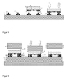
- a substrate 1 is shown, which may be, for example, a wafer with integrated circuits (not shown).
- the wafer is equipped at the appropriate points with a survey 3 'for the subsequent sealing frame and with Kunststoffbumps 4', which have different heights (see also reference numeral 6).
- Already isolated chips 2 carry respective elevations 3, 4, which are later joined together with the elevations 3 ', 4' or to electrically conductive connections and the sealing frame.
- the raised contacts 6 serve to adjust the gap height.
- 5 schematically indicates an active structure, for example a (movable) sensor.
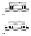
- FIG. 2 The sealing and contacting process is in FIG. 2 shown.
- a heatable on demand plate 7 supports the substrate 1, a heatable pressure plate 8 is moved to a distance 10 on the or the chips.
- the distances between the contact bumps or the parts provided for the sealing frame are chosen so that after the pre-fixing a circumferential gap 9 has remained, pulled by the gas from the chamber surrounding the active structure and / or introduced by the targeted a selected gas mixture can.
- the pressure plate 8 with the force F lowered, wherein the electrical connection contacts 11 and the hermetic sealing frame 12 form with metallurgical joining zone. Then the press is opened.
- FIG. 3 a variant of a sealing frame is shown, which is formed of two parts with interlocking ring structure 13. As explained in the description, this embodiment serves the passive orientation and the protection against slipping.
- FIG. 4 visualizes an embodiment of the invention in which both the Needlesbumps and the sealing frame are formed by the fact that metallic bumps and / or a metallic frame elevation 20 are applied to the substrate, which does not melt during subsequent joining, but can absorb excess eutectic, the the joining zone is pressed.
- copper is suitable.
- Gold is undersized on the copper bumps (designated by reference numeral 19).
- the chip-side elevations 21 are made of silicon and are usually defined by etching trenches. Due to the reduced cross section of the gold plating, the amount of molten metal (AuSi eutectic) formed during joining is reduced.
- a bonding pad 14 is shown which is connected to the contacts by a conductive structure (not shown) extending in the substrate. The active structure can be controlled via this bond pad outside the housing and the signals generated by it, possibly already processed, can be forwarded.
- a reduction of the molten metal can also be found in the FIG. 5 achieve embodiment shown.
- a thin layer of tin is applied in undersize to the gold elevations (denoted by 18).
- AuSn eutectic form Only small amounts of AuSn eutectic form.
- FIGS. 6 and 7 Two specific embodiments of components show the FIGS. 6 and 7 ,
- gas-specific sensor has a sealing frame, in the laterally continuous material 17 is installed with increased permeability to a gas.
- This material can be, for example, palladium, SiO 2 or carbon nanotubes and is permeable to a specific gas such as hydrogen, helium or gaseous water. This makes it possible to realize components that can measure the concentration of such gases undisturbed by other ambient conditions.
- FIG. 7 shown variant shows a device which is provided with a Substratlochung 15, the access of an ambient medium in the Space allowed that surrounds one of several active structures.
- the perforation can be covered with a (porous) membrane or a polymer layer 16, which can, for example, prevent particles or other unwanted constituents of the ambient atmosphere or of the ambient fluid.
- a membrane or a polymer layer 16 which can, for example, prevent particles or other unwanted constituents of the ambient atmosphere or of the ambient fluid.
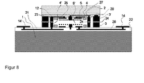
- FIG. 8 a variant of the invention is schematically shown, which has a second active structure 5 'on the surface of the substrate 1 and in which the electrical connection from the active structure 5 in the lid 2 to a bonding pad 14' outside the sealing frame is shown.
- the chip 2 is provided with an insulating support 23 into which a first electrical connection 25 leads from a first electrode of the sensor 5 to a first contact bump 4.
- the latter is in an electrically conductive contact (vertical contact) via a suitable metallic connection with a contact bump 4 'arranged opposite to it on the substrate, for example via a joining material 24 such as an AuSn alloy, if the contact bumps are those made of gold. as described above.
- an insulating pad 22 of the substrate 1 is also an electrical conduction structure or an integrated circuit 21 buried, which leads to a bonding pad 14 'outside the sensor housing.
- the contact bump 4 ' is connected to the electrical line structure 21 in the substrate, so that an electrode or electrode group of the chip sensor 5 can be electrically driven from outside the sensor cavity and / or tapped, possibly after suitable processing of the electrical signal in the circuit in the substrate ,
- the counterelectrode of the active structure 5 in the chip 2 is electrically connected in a comparable manner via a further electrical connection 27 in the insulating layer 23 and the electrically interconnected contact points 4, 4 'on the cover and the substrate side within the sealing frame with a bonding pad (not shown) connected.
- the second active structure which is located on the substrate and which is here again exemplarily indicated in the form of a sensor 5 ', is contacted via further interconnects buried in the insulating layer 22 of the substrate 1 or integrated circuits on bond pads outside the sealing frame where only the right side trace 26 and the bonding pad 14 are shown.
- the sealing frame which can perform purely mechanical tasks, but if necessary, could also be used for electrical connections, is in this Variant as constructed of the same materials (in the form of a frame metallization 3, 24, 3 ') shown as the contact structure 4, 24, 4' between the chip and the substrate. A possible or necessary external insulation is not shown.
- the cavity in which the two (or more) sensors are included may include a getter material, such as a patterned thin film getter 12 on surfaces of the chip and / or substrate not covered by the sensors and not required.
- a getter material such as a patterned thin film getter 12 on surfaces of the chip and / or substrate not covered by the sensors and not required.
- the reference numeral 28 indicates a variant - only on the right-hand side of this figure.
- a contacting structure 28 may be provided in the region of the sealing frame or in the region of a vertical contact (not shown) which comprises the substrate crystal of the upper sensor Earth potential (or any controlled potential) sets and thus can prevent electrical charging effects.
Landscapes
- Engineering & Computer Science (AREA)
- Microelectronics & Electronic Packaging (AREA)
- Manufacturing & Machinery (AREA)
- Wire Bonding (AREA)
- Micromachines (AREA)
Applications Claiming Priority (2)
| Application Number | Priority Date | Filing Date | Title |
|---|---|---|---|
| DE102007016608 | 2007-04-05 | ||
| DE102007047771 | 2007-10-05 |
Publications (2)
| Publication Number | Publication Date |
|---|---|
| EP1977991A2 true EP1977991A2 (fr) | 2008-10-08 |
| EP1977991A3 EP1977991A3 (fr) | 2013-08-14 |
Family
ID=39708728
Family Applications (1)
| Application Number | Title | Priority Date | Filing Date |
|---|---|---|---|
| EP20080154171 Ceased EP1977991A3 (fr) | 2007-04-05 | 2008-04-07 | Composants microstructurés dotés d'un substrat et d'une puce mise en contact direct avec le substrat, et son procédé de fabrication |
Country Status (1)
| Country | Link |
|---|---|
| EP (1) | EP1977991A3 (fr) |
Cited By (1)
| Publication number | Priority date | Publication date | Assignee | Title |
|---|---|---|---|---|
| DE102009000048A1 (de) * | 2009-01-07 | 2010-07-08 | Robert Bosch Gmbh | Mikrotechnisches System und Verfahren zur Herstellung eines mikrotechnischen Systems |
Citations (1)
| Publication number | Priority date | Publication date | Assignee | Title |
|---|---|---|---|---|
| DE102005026243A1 (de) * | 2005-06-07 | 2006-12-14 | Epcos Ag | Elektrisches Bauelement und Herstellungsverfahren |
Family Cites Families (4)
| Publication number | Priority date | Publication date | Assignee | Title |
|---|---|---|---|---|
| EP0886144B1 (fr) * | 1997-06-19 | 2006-09-06 | STMicroelectronics S.r.l. | Capteur scellé hermétiquement avec microstructure mobile |
| US6853067B1 (en) * | 1999-10-12 | 2005-02-08 | Microassembly Technologies, Inc. | Microelectromechanical systems using thermocompression bonding |
| DE102004027501A1 (de) * | 2004-06-04 | 2005-12-22 | Robert Bosch Gmbh | Mikromechanisches Bauelement mit mehreren Kavernen und Herstellungsverfahren |
| US7442570B2 (en) * | 2005-03-18 | 2008-10-28 | Invensence Inc. | Method of fabrication of a AL/GE bonding in a wafer packaging environment and a product produced therefrom |
-
2008
- 2008-04-07 EP EP20080154171 patent/EP1977991A3/fr not_active Ceased
Patent Citations (1)
| Publication number | Priority date | Publication date | Assignee | Title |
|---|---|---|---|---|
| DE102005026243A1 (de) * | 2005-06-07 | 2006-12-14 | Epcos Ag | Elektrisches Bauelement und Herstellungsverfahren |
Non-Patent Citations (1)
| Title |
|---|
| C. SCHEIRING ET AL.: "Advanced-Chip-to Wafer Technology: Enabling Technology for Volume Production of 3D System Integration on Wafer Level", IMAPS, 2004 |
Cited By (1)
| Publication number | Priority date | Publication date | Assignee | Title |
|---|---|---|---|---|
| DE102009000048A1 (de) * | 2009-01-07 | 2010-07-08 | Robert Bosch Gmbh | Mikrotechnisches System und Verfahren zur Herstellung eines mikrotechnischen Systems |
Also Published As
| Publication number | Publication date |
|---|---|
| EP1977991A3 (fr) | 2013-08-14 |
Similar Documents
| Publication | Publication Date | Title |
|---|---|---|
| DE102008025599B4 (de) | Gehäuste aktive Mikrostrukturen mit Direktkontaktierung zu einem Substrat | |
| DE102009029180B4 (de) | Mikrosystem | |
| EP2004542B1 (fr) | Boîtier micromécanique comportant au moins deux cavités présentant des pressions intérieures et/ou des compositions gazeuses différentes et procédé de fabrication | |
| DE102012108305B4 (de) | Sensorbauelement und Verfahren | |
| DE102010039057B4 (de) | Sensormodul | |
| EP2170763B1 (fr) | Procédé de production d'un composant, et composant obtenu | |
| DE102007063742B4 (de) | Sensor für eine physikalische Größe | |
| DE102015102869B4 (de) | MEMS-Bauelement mit hoher Integrationsdichte und Verfahren zu seiner Herstellung | |
| DE102007060931A1 (de) | Verkapselungsmodul, Verfahren zu dessen Herstellung und Verwendung | |
| EP1869705B1 (fr) | Procédé de fabrication de dispositifs électroniques en boîtier et dispositif électronique en boîtier | |
| DE102007050865A1 (de) | Funktionsbauteil | |
| WO2003038449A1 (fr) | Microcapteur | |
| DE102014210006A1 (de) | Sensoreinheit und Verfahren zur Herstellung einer Sensoreinheit | |
| DE102009038706A1 (de) | Sensorbauelement | |
| DE102016216207A1 (de) | Verfahren zum Herstellen eines mikromechanischen Sensors | |
| DE102014202808A1 (de) | Verfahren zum eutektischen Bonden zweier Trägereinrichtungen | |
| EP1945563B1 (fr) | Composant pouvant etre employe dans des microsystemes et procede de soudage destine a la connexion de parties correspondantes de plaquette ou de composant | |
| DE10324421B4 (de) | Halbleiterbauelement mit Metallisierungsfläche und Verfahren zur Herstellung desselben | |
| EP1977991A2 (fr) | Composants microstructurés dotés d'un substrat et d'une puce mise en contact direct avec le substrat, et son procédé de fabrication | |
| DE102009000058A1 (de) | Sensoranordnung und Verfahren zur Herstellung einer Sensoranordnung | |
| DE102007001290A1 (de) | Halbleitermodul | |
| DE10350460A1 (de) | Verfahren zum Verbinden prozessierter Halbleiterscheiben bei dem neben dem festen isolierenden Zusammenfügen auch eine elektrische Verbindung hergestellt wird und entsprechende Anordnung | |
| DE102023211180A1 (de) | Mikroelektromechanischer Drucksensor und Verfahren zur Herstellung eines mikroelektromechanischen Drucksensors | |
| DE102021204645A1 (de) | Verfahren zur Herstellung eines mikroelektromechanischen Sensors aus einem MEMS-Element und einem ASIC-Element und mikroelektromechanischer Sensor | |
| DE102007060785B4 (de) | Verfahren zur Herstellung eines (Vielfach-) Bauelements auf Basis ultraplanarer Metallstrukturen |
Legal Events
| Date | Code | Title | Description |
|---|---|---|---|
| PUAI | Public reference made under article 153(3) epc to a published international application that has entered the european phase |
Free format text: ORIGINAL CODE: 0009012 |
|
| AK | Designated contracting states |
Kind code of ref document: A2 Designated state(s): AT BE BG CH CY CZ DE DK EE ES FI FR GB GR HR HU IE IS IT LI LT LU LV MC MT NL NO PL PT RO SE SI SK TR |
|
| AX | Request for extension of the european patent |
Extension state: AL BA MK RS |
|
| PUAL | Search report despatched |
Free format text: ORIGINAL CODE: 0009013 |
|
| AK | Designated contracting states |
Kind code of ref document: A3 Designated state(s): AT BE BG CH CY CZ DE DK EE ES FI FR GB GR HR HU IE IS IT LI LT LU LV MC MT NL NO PL PT RO SE SI SK TR |
|
| AX | Request for extension of the european patent |
Extension state: AL BA MK RS |
|
| RIC1 | Information provided on ipc code assigned before grant |
Ipc: B81C 1/00 20060101AFI20130710BHEP |
|
| 17P | Request for examination filed |
Effective date: 20140131 |
|
| RBV | Designated contracting states (corrected) |
Designated state(s): AT BE BG CH CY CZ DE DK EE ES FI FR GB GR HR HU IE IS IT LI LT LU LV MC MT NL NO PL PT RO SE SI SK TR |
|
| RBV | Designated contracting states (corrected) |
Designated state(s): AT BE BG CH CY CZ DE DK EE ES FI FR GB GR HR HU IE IS IT LI LT LU LV MC MT NL NO PL PT RO SE SI SK TR |
|
| AKX | Designation fees paid |
Designated state(s): AT BE BG CH CY CZ DE DK EE ES FI FR GB GR HR HU IE IS IT LI LT LU LV MC MT NL NO PL PT RO SE SI SK TR |
|
| 17Q | First examination report despatched |
Effective date: 20150506 |
|
| STAA | Information on the status of an ep patent application or granted ep patent |
Free format text: STATUS: THE APPLICATION HAS BEEN REFUSED |
|
| 18R | Application refused |
Effective date: 20171016 |