EP1978611A1 - Microlaser à déclenchément et procédé d'utilisation - Google Patents
Microlaser à déclenchément et procédé d'utilisation Download PDFInfo
- Publication number
- EP1978611A1 EP1978611A1 EP08075247A EP08075247A EP1978611A1 EP 1978611 A1 EP1978611 A1 EP 1978611A1 EP 08075247 A EP08075247 A EP 08075247A EP 08075247 A EP08075247 A EP 08075247A EP 1978611 A1 EP1978611 A1 EP 1978611A1
- Authority
- EP
- European Patent Office
- Prior art keywords
- microlaser
- heat spreader
- gain medium
- wavelength
- saturable absorber
- Prior art date
- Legal status (The legal status is an assumption and is not a legal conclusion. Google has not performed a legal analysis and makes no representation as to the accuracy of the status listed.)
- Granted
Links
Images

Classifications
-
- H—ELECTRICITY
- H01—ELECTRIC ELEMENTS
- H01S—DEVICES USING THE PROCESS OF LIGHT AMPLIFICATION BY STIMULATED EMISSION OF RADIATION [LASER] TO AMPLIFY OR GENERATE LIGHT; DEVICES USING STIMULATED EMISSION OF ELECTROMAGNETIC RADIATION IN WAVE RANGES OTHER THAN OPTICAL
- H01S3/00—Lasers, i.e. devices using stimulated emission of electromagnetic radiation in the infrared, visible or ultraviolet wave range
- H01S3/10—Controlling the intensity, frequency, phase, polarisation or direction of the emitted radiation, e.g. switching, gating, modulating or demodulating
- H01S3/11—Mode locking; Q-switching; Other giant-pulse techniques, e.g. cavity dumping
- H01S3/1106—Mode locking
- H01S3/1112—Passive mode locking
- H01S3/1115—Passive mode locking using intracavity saturable absorbers
-
- H—ELECTRICITY
- H01—ELECTRIC ELEMENTS
- H01S—DEVICES USING THE PROCESS OF LIGHT AMPLIFICATION BY STIMULATED EMISSION OF RADIATION [LASER] TO AMPLIFY OR GENERATE LIGHT; DEVICES USING STIMULATED EMISSION OF ELECTROMAGNETIC RADIATION IN WAVE RANGES OTHER THAN OPTICAL
- H01S3/00—Lasers, i.e. devices using stimulated emission of electromagnetic radiation in the infrared, visible or ultraviolet wave range
- H01S3/02—Constructional details
- H01S3/04—Arrangements for thermal management
- H01S3/042—Arrangements for thermal management for solid state lasers
-
- H—ELECTRICITY
- H01—ELECTRIC ELEMENTS
- H01S—DEVICES USING THE PROCESS OF LIGHT AMPLIFICATION BY STIMULATED EMISSION OF RADIATION [LASER] TO AMPLIFY OR GENERATE LIGHT; DEVICES USING STIMULATED EMISSION OF ELECTROMAGNETIC RADIATION IN WAVE RANGES OTHER THAN OPTICAL
- H01S3/00—Lasers, i.e. devices using stimulated emission of electromagnetic radiation in the infrared, visible or ultraviolet wave range
- H01S3/05—Construction or shape of optical resonators; Accommodation of active medium therein; Shape of active medium
- H01S3/06—Construction or shape of active medium
- H01S3/0627—Construction or shape of active medium the resonator being monolithic, e.g. microlaser
-
- H—ELECTRICITY
- H01—ELECTRIC ELEMENTS
- H01S—DEVICES USING THE PROCESS OF LIGHT AMPLIFICATION BY STIMULATED EMISSION OF RADIATION [LASER] TO AMPLIFY OR GENERATE LIGHT; DEVICES USING STIMULATED EMISSION OF ELECTROMAGNETIC RADIATION IN WAVE RANGES OTHER THAN OPTICAL
- H01S3/00—Lasers, i.e. devices using stimulated emission of electromagnetic radiation in the infrared, visible or ultraviolet wave range
- H01S3/10—Controlling the intensity, frequency, phase, polarisation or direction of the emitted radiation, e.g. switching, gating, modulating or demodulating
- H01S3/11—Mode locking; Q-switching; Other giant-pulse techniques, e.g. cavity dumping
- H01S3/1123—Q-switching
- H01S3/113—Q-switching using intracavity saturable absorbers
-
- H—ELECTRICITY
- H01—ELECTRIC ELEMENTS
- H01S—DEVICES USING THE PROCESS OF LIGHT AMPLIFICATION BY STIMULATED EMISSION OF RADIATION [LASER] TO AMPLIFY OR GENERATE LIGHT; DEVICES USING STIMULATED EMISSION OF ELECTROMAGNETIC RADIATION IN WAVE RANGES OTHER THAN OPTICAL
- H01S3/00—Lasers, i.e. devices using stimulated emission of electromagnetic radiation in the infrared, visible or ultraviolet wave range
- H01S3/02—Constructional details
- H01S3/04—Arrangements for thermal management
- H01S3/0405—Conductive cooling, e.g. by heat sinks or thermo-electric elements
-
- H—ELECTRICITY
- H01—ELECTRIC ELEMENTS
- H01S—DEVICES USING THE PROCESS OF LIGHT AMPLIFICATION BY STIMULATED EMISSION OF RADIATION [LASER] TO AMPLIFY OR GENERATE LIGHT; DEVICES USING STIMULATED EMISSION OF ELECTROMAGNETIC RADIATION IN WAVE RANGES OTHER THAN OPTICAL
- H01S3/00—Lasers, i.e. devices using stimulated emission of electromagnetic radiation in the infrared, visible or ultraviolet wave range
- H01S3/05—Construction or shape of optical resonators; Accommodation of active medium therein; Shape of active medium
- H01S3/08—Construction or shape of optical resonators or components thereof
- H01S3/08072—Thermal lensing or thermally induced birefringence; Compensation thereof
-
- H—ELECTRICITY
- H01—ELECTRIC ELEMENTS
- H01S—DEVICES USING THE PROCESS OF LIGHT AMPLIFICATION BY STIMULATED EMISSION OF RADIATION [LASER] TO AMPLIFY OR GENERATE LIGHT; DEVICES USING STIMULATED EMISSION OF ELECTROMAGNETIC RADIATION IN WAVE RANGES OTHER THAN OPTICAL
- H01S3/00—Lasers, i.e. devices using stimulated emission of electromagnetic radiation in the infrared, visible or ultraviolet wave range
- H01S3/09—Processes or apparatus for excitation, e.g. pumping
- H01S3/091—Processes or apparatus for excitation, e.g. pumping using optical pumping
- H01S3/094—Processes or apparatus for excitation, e.g. pumping using optical pumping by coherent light
- H01S3/0941—Processes or apparatus for excitation, e.g. pumping using optical pumping by coherent light of a laser diode
- H01S3/09415—Processes or apparatus for excitation, e.g. pumping using optical pumping by coherent light of a laser diode the pumping beam being parallel to the lasing mode of the pumped medium, e.g. end-pumping
Definitions
- the process of Q-switching involves the introduction of loss, for example with the use of an absorber or shutter, in a laser oscillator sufficient to prevent lasing while energy is being transferred to a gain medium.
- loss for example with the use of an absorber or shutter
- an intense photon flux builds exponentially from spontaneous emission and the coupling of these photons through a partially reflecting resonator mirror leads to the generation of a Q-switched laser pulse.
- Q-switched laser pulses have been as short as several tens of picoseconds or as long as several hundred nanoseconds, with pulse energies that may range from a small fraction of a microjoule to a significant fraction of a Joule.
- the advent of diode laser pumped solid-state lasers and solid-state saturable absorbers has generated renewed interest in passively Q-switched lasers, including microlasers.
- passive Q-switching the laser resonator contains a gain medium and an absorbing medium, both may be saturable and therefore nonlinear in response.
- the gain medium As the gain medium is pumped, it may both accumulate stored energy and emit photons. Over many round trips within the laser resonator the photon flux may see gain, fixed loss, and saturable loss in the absorber.
- the photon flux may build but the laser will not emit intense pulses.
- the photon flux builds up to a level that saturates or bleaches the absorber first, the resonator sees a dramatic reduction in intracavity loss and the laser Q-switches, thereby generating a short intense pulse of light.
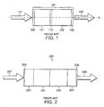
- the passively Q-switched microlaser 100 includes a gain medium 101 bonded to a saturable absorber 102 enclosed by a pair of dielectric coatings, 105 and 106, that form a resonant cavity.
- the dielectric coating 105 on the gain medium transmits the pump light, provided by a light source 114, and is highly reflecting (the high reflector) at the microlaser wavelength.
- the dielectric coating 106 on the saturable absorber is partially reflecting (the output coupler) at the microlaser wavelength and provides the optical output 108 from the microlaser.
- the faces of the gain medium 101 and the saturable absorber 102 that form the interface 112 may be coated dielectrically so as to reflect unabsorbed pump light back through the gain medium and transmit light at the microlaser wavelength.
- the single crystal material microlasers may be optically pumped at powers up to several Watts, which may result in the occurrence of optical damage.
- the optical damage may be in the form of either bulk crystal fracture or optical coating failure as a result of thermally induced stress lowering the coating damage threshold.
- some applications require passively Q-switched microlasers to operate with higher pump powers than is possible in a simple device without improved heat removal.
- Heat loads in the gain medium and saturable absorber of the conventional passively Q-switched microlaser are generally removed via conduction through one, or more, of the sides of thc device that arc not optically active.
- the lack of more direct heat removal from the optically active pumped face of the gain medium, and to a lesser extent the microlaser output face of the saturable absorber, can limit the maximum average pump power and output power of the device to levels below those desired for some applications.
- the power limiting mechanism is catastrophic thermal fracture of the materials that constitute the laser because of excessive thermally induced stress.
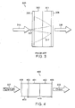
- the Zayhowski et al. system includes a microlaser 200 comprising a monolithic assembly of a Nd:YAG gain medium 201, a Cr:YAG saturable absorber 202, and two undoped YAG end caps, 203 and 204, all bonded together using diffusion bonding according to US Patent 5,846,638 .
- the two undoped YAG end caps, 203 and 204 were coated dielectrically, with coatings 205 and 206 respectively, to provide the same high reflector and output coupler mirror actions described above and thereby form a resonant optical cavity.
- the dielectric coating 205 will transmit the pump light 207 and reflect light at the microlaser wavelength
- the dielectric coating 206 will reflect the pump light and partially reflect light at the microlaser wavelength producing an output beam 208.
- the undoped YAG end caps act as heat spreaders and arc contained within the microlaser resonator and contribute to its total optical path length.
- the optical path length determines the microlaser pulse duration.
- Karlsson et al. experienced thermal fracture of a phosphate glass laser host at average pump powers as low as 740 mW. Initially Karlsson et al. attempted to resolve this problem by developing a phosphate laser glass with higher thermal conductivity [ Karlsson et al.: "Development and characterization of Yb-Er laser glass for high average power laser diode pumping," Appl. Phys. B, vol 75, pp. 41-46 (2002 )], but eventually settled on the solution disclosed in Laurell et al., US Patent 6,778,563 ( Fig. 3 ).
- FIG. 3 illustrates a passively Q-switched Yb,Er:glass microlaser 300 that includes a gain medium 301 bonded to a saturable absorber 302 enclosed by a pair of dielectric coatings 305 and 306, that form a resonant cavity.
- the dielectric coating 305 on the saturable absorber 302 transmits the pump light 307 emitted from a diode laser 314 and is highly reflecting (the high reflector) at the microlaser wavelength.
- the dielectric coating 306 on the gain medium 301 is partially reflecting (the output coupler) at the microlaser wavelength and provides the optical output 308 from the microlaser.
- the output coupler coating 306 also reflects unabsorbed pump light 307 back through the gain medium 301.
- the saturable absorber 302 does not absorb the pump light 307 but instead transmits the pump light, the absorber acts as a heat spreader to allow for the use of higher pump powers.
- the saturable absorber 302 acts as a heat spreader, this method has only been applied to this one case because it requires the use of a saturable absorber, in this case Co:spinel, that transmits the pump light.
- a saturable absorber in this case Co:spinel
- the same method cannot be applied to the widely used Nd:YAG/Cr:YAG passively Q-switched microlaser system because the saturable absorber, Cr:YAG, absorbs pump light as strongly as the gain medium, Nd:YAG.
- a passively Q-switched microlaser One of the primary reasons to use a passively Q-switched microlaser is to generate short duration, high-peak power pulses. These pulses may range from several hundred picoseconds to two or three nanoseconds long depending on the choice of gain medium, saturable absorber and resonator physical characteristics. Adding additional length to the resonator of a passively Q-switched microlaser, in the form of an optically transparent element (i.e. providing neither gain nor loss of any type), will always lead to an increase in the Q-switched pulse durations. This increase in Q-switched pulse durations is in direct proportion to the increase in resonator length.
- Zayhowski et al have demonstrated several passively Q-switched Nd:YAG/Cr:YAG microlasers with pulse durations in the 200 ps to 300 ps range without undoped YAG end caps that increased to 300 ps to 400 ps when 0.5 mm thick undoped YAG end caps were added.
- the saturable absorber dissipates heat because of the absorption of laser radiation during the bleaching process.
- the saturable absorber may also absorb a fraction of the residual pump light exiting the gain medium, for example such is the case of a Cr:YAG saturable absorber in an 808-nm pumped Nd:YAG gain medium. Hence, there may also he significant heat loads that need to be removed from the saturable absorber end of the microlaser.
- Passively Q-switched microlasers require improved heat removal to allow them to be reliably operated at higher average powers, which generally means higher pulse repetition rates, without causing thermal stress induced fracture of the laser gain medium or saturable absorber, which would result in catastrophic failure of the laser.
- a passively Q-switched laser apparatus comprises an optically transparent heat conductive element that may be bonded to a gain medium, which in turn may be bonded to a saturable absorber.
- the saturable absorber may also be bonded to a second optically transparent heat conductive element. Only the gain medium and saturable absorber are disposed within a resonant cavity formed by optical coatings located in the bond interfaces.
- the optically transparent heat conductive element, or elements serve to efficiently conduct heat from the optical beam path of the microlaser resonator without interfering with the pump light or the microlaser beam paths. In particular, because the optically transparent heat conductive elements lie outside the microlaser resonator they do not add to the resonator optical path length.
- An advantage of the embodiment is to allow higher optical pump powers to be used to provide access to a larger range of pulse repetition rates, which is particularly useful in applications that require the collection of many individual single pulse data. For example, in ranging or range imaging applications.
- Higher pump powers enable the generation of higher pulse repetition rates because the pump energy required to generate a single Q-switched microlaser pulse is essentially fixed and is therefore delivered in a shorter time at higher pump powers.
- Another advantage of the embodiment is that the use of a heat spreader arrangement leads to significantly reduced thermal lensing and optical distortion in the gain medium and saturable absorber elements thereby improving the output beam quality of the microlaser, especially at higher pump powers. This characteristic is particularly important when using glass host media because of their relatively poor thermal conductivity.
- the optically transparent heat conductive element may be chosen to specifically transmit either the pump light wavelength or the microlaser output wavelength, while absorbing the other as a means to prevent unwanted pump light from reaching the output beam path or to prevent microlaser pulse energy from reaching and possibly damaging the pump light source, which is typically a semiconductor diode laser.
- the passively Q-switched microlaser arrangement may comprise a monolithic body including a layer of optically pumped gain medium, a layer of saturable absorber, first and second reflectors arranged to enclose the gain medium and the saturable absorber in order to form a resonant cavity having an optical axis, a heat spreader of optically transparent material on the optic axis outside of the resonate cavity, and an optical pump beam at a wavelength absorbed by the gain medium arranged for longitudinal pumping of said laser resonator.
- the gain medium active ion may be Nd 3+ , Er 3+ , Ho 3+ , Tm 3+ , Yb 3+ , or a combination thereof.
- the gain medium may also be comprised of a single crystal host material that is a member of the garnet, fluoride, orthovanadate, tungstate, or oxyborate families.
- the gain medium host material may also be a phosphate glass, a silicate glass, or an optical ceramic, such as ceramic YAG.
- the gain medium may be Nd:YAG or Yb,Er co-doped phosphate glass.
- the saturable absorber active ion may be Cr 4+ or Co 2+ .
- the saturable absorber may comprise a host material which is a single crystal material that may be a member of the garnet, fluoride, orthovanadate, tungstate, or oxyborate families.
- the saturable absorber host material may also be a phosphate glass, a silicate glass, or an optical ceramic, such as ceramic YAG.
- the saturable absorber may also be Cr:YAG or Co:spinel.
- the heat spreader may be a single crystal material that is a member of the garnet, fluoride, orthovanadate, tungstate, or oxyborate families.
- the heat spreader may also be sapphire or Co:spinel,
- the heat spreader may be configured to transmit light at the pump laser wavelength and absorb light at the microlaser wavelength or vice-versa.
- the heat spreader may also be configured to remove heat from an optically pumped surface.
- the microlaser may also comprise two heat spreaders, the second heat spreader being located on the optical axis and outside of the resonant cavity, with the heat spreader and second heat spreader being on opposite ends of the resonant cavity.
- the first and second reflectors may be dielectric coatings applied directly to the gain medium and saturable absorber, respectively.
- the first and second reflectors may also be mirrors attached to the gain medium and saturable absorber by adhesives or bonding techniques.
- the first reflector may be configured to transmit light at the pump laser wavelength and reflect light at the microlaser wavelength.
- the second reflector may be configured to reflect light at the pump laser wavelength and partially transmit light at the microlaser wavelength.
- the gain medium, saturable absorber and heat spreader material may use a common host crystal.
- the common host crystal may be a single crystal material that is a member of the garnet, fluoride, orthovanadate, tungstate or oxyborate families.
- the apparatus may comprise an optically transparent heat conductive element that may be bonded to a gain medium, which in turn may be bonded to a saturable absorber.
- the saturable absorber may also be bonded to a second optically transparent heat conductive element. Only the gain medium and saturable absorber are disposed within a resonant cavity formed by optical coatings located in the bond interfaces.
- the optically transparent heat conductive element, or elements serve to efficiently conduct heat from the optical beam path of the microlaser resonator without interfering with the pump light or the microlaser beam paths.
- the optically transparent heat conductive elements lie outside the microlaser resonator they do not add to the resonator optical path length.
- the methods and apparatus presented herein provide a low cost and casily manufactured solution to heat removal in passively Q-switched microlasers.
- the methods and apparatus presented herein also allow for higher pumping powers resulting in higher pulse repetition rates without increasing the duration of the pulse.
- the expression “optically transparent” refers to an optical element that provides minimal or no optical gain and no significant loss at the wavelength of the light being intentionally transmitted.
- the light being transmitted will be at either the pump light wavelength or microlaser output wavelength, or both, depending on the location of the element.
- the element does not need to be optically transparent at other less significant wavelengths.
- heat spreader and “optically transparent heat conductive element” may be used interchangeably within the context of describing the present invention.
- FIG. 4 schematically illustrates a passively Q-switched microlaser 400 according to an embodiment of the present invention.
- the passively Q-switched microlaser 400 comprises a gain medium 401 bonded to a saturable absorber 402 enclosed by a pair of dielectric coatings, 405 and 406, that form a resonant cavity defined by a length 410.
- the dielectric coating 405 on the gain medium 401 transmits the pump light 407 and is highly reflecting (the high reflector) at the microlaser wavelength.
- the dielectric coating 406 on the saturable absorber 402 is partially reflecting (the output coupler) at the microlaser wavelength and provides an optical output 408 from the microlaser 400.
- the output coupler coating 406 may also reflect unabsorbed pump light 407 back though the gain medium 401.
- An optically transparent heat conductive element 403 is bonded to the gain medium 401 and its exposed face dielectrically coated 409. It is important to note that the dielectric coating 409 on the optically transparent heat conductive element 403 plays no role in formation of the microlaser resonant optical cavity, and does not add to the resonator optical length 410. Therefore, the optically transparent heat conductive element 403 does not influence the performance of the micro laser 400, for example, by altering the duration of the pulses.
- the transmitted light will then pass through the gain medium 401, thus causing an excitation of ions and energy to be stored within the gain medium 401.
- the absorber 402 will become saturated causing a reduction in resonator loss and a rapid further increase in intensity and the extraction of a significant fraction of the stored energy as the microlaser output pulse.
- the absorber 402 may recover to its high-loss state before the gain medium 401 recovers, so that the next pulse is delayed until the stored energy in the gain medium 401 is fully replenished.
- the physical properties of the saturable absorber and gain medium largely determine the repetitive nature of the Q-switched pulse generation when the pump light is continuous.
- the optically transparent heat conductive element 403 brings many advantageous features to the microlaser 400, one of which is to act as a heat spreader. Heat removal from the gain medium via direct conduction through the heat spreader significantly reduces the peak temperature, temperature gradients and thermally induced stress in the gain medium 401.
- the microlaser 500 also comprises dielectric coatings 505 and 506 defining the limits of the resonator optical length 510.
- the optically transparent heat conductive element 503 also comprises a dielectric coating 509.
- the microlaser 500 is adapted to receive a pump light 507 and emit an output light beam 508.
- the absorption of pump light 507 in the gain medium 501 may result in a significant rise in temperature of the pumped surface 520.
- the heat spreader 503 may be used to remove the heat from the pumped surface 520, thereby reducing its temperature as represented by heat flux lines 513. Once the flux lines 51.3 reach the heat spreader 503, they diverge representing a decrease in temperature due to a spreading of heat.
- An aluminum plate 511 held at 25°C is used as a heat sink, thus all the dispersed heat 513 will be transferred to the aluminum plate 511.
- the heat load in the gain medium 501 was confined to a 100 ⁇ m diameter region typical of the pumped region cross-sectional area of a longitudinally pumped microlaser.
- the optically transparent heat conductive element 403 may also, protect the source of the pump light.
- the semiconductor diode laser pump source used with a passively Q-switched microlaser may in some instances be optically damaged by microlaser pulse energy that is transmitted via the microlaser resonator high reflector.
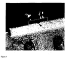
- Figure 7 shows a microscope photograph of a 975 nm single emitter diode laser that ceased to emit after being used to optically pump a passively Q-switched Yb,Er:glass microlaser.
- the center of the device facet that is outlined by a rectangle has a circular pit, or damage site, located in the emitting region.
- This damage site is a result of material ablation by several thousand 1.5 ⁇ m, 1 ⁇ J to 2 ⁇ J laser pulses. Normally one expects that very little if any laser pulse energy would be emitted via the high reflector of the microlaser.
- the output coupler transmission is typically only 1% for a Yb,Er:glass passively Q-switched microlaser and such a micro laser generating 10 ⁇ J to 20 ⁇ J output pulse energies with even a 99.9% reflectivity high reflector would leak sufficient pulsed energy to be problematic.
- the optically transparent heat conductive element 403 may be used to prevent microlaser pulse energy leakage via the high reflector by one of two methods or a combination of the two.
- the first method is by designing the dielectric coating 409 on the exposed surface of the heat spreader 403 to be highly reflective at the microlaser wavelength. This method has the potential for the formation of an optical etalon between the dielectric coatings on the heat spreader 403 and the gain medium 401, which can be eliminated by wedging the heat spreader.
- a sapphire heat spreader was bonded with a thin layer of UV-cure optical adhesive to the pumped face of the passively Q-switched microlaser that caused the damage shown in the Figure 7 .
- the exposed surface of the sapphire heat spreader was dielectrically coated to be highly reflective at the microlaser wavelength. This laser was then operated for many hours over a period of several weeks with a replacement semiconductor diode laser as the pump source without subsequent failure of, or damage to, the diode laser.
- the second method is by use of a heat spreader 403 that is absorbing at the microlaser wavelength and transmitting at the pump wavelength, which in the case of the Yb,Er:glass laser example could be the saturable absorber, Co:apinel.
- the bonding method used to attach the different elements of the microlaser to one another need to be compatible with the materials used. Particular attention should be paid to mismatches in the coefficient of thermal expansion and melting point to ensure the formation of strong, low optical loss and stress free interfaces. Bonding methods that may be used include, but are not limited to, optical contacting, adhesive bonding, diffusion bonding, fusion bonding, wringing, frit bonding, and chemically assisted direct bonding. Many bonding methods introduce no material, or very little material, between the components being bonded and therefore do not significantly contribute to thermal resistance.
- the heat spreader will have the same, or larger, cross-sectional area as the gain medium surface of the microlaser and will typically be between 0.1 mm and 10.0 mm thick. Thinner heat spreaders are difficult to fabricate and do not effectively remove heat, while thicker heat spreaders are no more effective than those that fall in the stated thickness range.
- Single crystal materials offer higher thermal conductivities than glasses or plastics when considered for use as a heat spreader.
- the commonly used optically transparent materials and their thermal conductivities given in Table 1 illustrate the superiority of single crystal materials for use as heat spreaders.
- the use of a glass material may be required for fabrication reasons and would be better than no heat spreader.
- Plastics and organic materials are generally of no use as heat spreaders, but may be successfully used in very thin layers as bonding adhesives.
- Table 1 Thermal conductivities of commonly used optically transparent materials including laser gain media host crystals and glasses.
- Preferred heat spreader materials are sapphire and undoped YAG because of their widespread availability.
- YAG is particularly useful as a heat spreading material because it is also widely used as the host material for many laser gain media (Nd:YAG, Yb:YAG, Tm:YAG, Ho:YAG, Er:YAG, Ho,Tm:YAG) and the most widely used 1-micron saturable absorber, Cr:YAG.
- this preference does not preclude the use of any other suitable materials should they become available.
- FIG. 6 schematically illustrates an alternative design for a passively Q-switched microlaser 600 according to an embodiment of the present invention.
- the microlaser 600 comprises a gain medium 601 bonded to a saturable absorber 602 enclosed by a pair of dielectric coatings, 605 and 606, that form a resonant cavity defined by an optical length 610.
- the dielectric coating 605, on the gain medium 601 transmits the pump light 607 and is highly reflecting (the high reflector) at the microlaser wavelength.
- the dielectric coating 606 on the saturable absorber 602 is partially reflecting (the output coupler) at the microlaser wavelength and provides the optical output beam 608 from the microlaser 600.
- the output coupler coating 606 may also reflect unabsorbed pump light back though the gain medium 601.
- a first optically transparent heat conductive element 603 is bonded to the gain medium 601 and the exposed face dielectrically coated 609, in a similar manner to that of the microlaser 400 of Figure 4 .
- the optically transparent heat conductive element 603 also acts as a heat spreader, thus reducing the temperature at the pump surface 620 and preventing thermal stress induced fracture of the gain medium 601 or optical damage to the dielectric coating 605, which would result in catastrophic failure of the microlaser 600.
- the first optically transparent heat conductive element 603 may be highly transmissive at the pump light wavelength and absorbing at the microlaser wavelength, thus preventing the microlaser pulse energy from reaching the pump light source and potentially causing damage. Additional protection may be provided for the pump source by making the dielectric coating 609 highly reflecting at the microlaser wavelength.
- a second optically transparent heat conductive element 604 may be bonded to the saturable absorber 602 and the exposed face dielectrically coated 615.
- the second optically transparent heat conductive element 604 may also act as a heat spreader and reduce the temperature at the surface 622 of the saturable absorber 602.
- the primary method of heat removal from the saturable absorber via direct conduction through the second heat spreader 604 is the same as described for the first heat spreader and is equally effective in reducing the peak temperature, temperature gradients and thermally induced stress.
- the second optically transparent heat conductive element 604 may also be used to prevent unabsorbed pump light 607 exiting the microlaser via the output coupler 606 with the intended output beam 608, which is undesirable, by the same techniques of reflection and absorption described as a means to prevent microlaser pulse energy from reaching the pump source 607.
- the dielectric coating 615 on the exposed surface of the second heat spreader 604 may be highly reflecting at the pump light wavelength, which removes the pump light 607 from the output beam 608 of the microlaser with the advantage that more pump light 607 is deposited in the gain medium 601 because of the second pass.
- Unabsorbed pump light may be also be attenuated by use of a heat spreader 604 that is absorbing at the pump light wavelength and transmitting at the microlaser wavelength, which in the case of the Yb,Er:glass laser example could be Yb:YAG.
- the dielectric coatings on the optically transparent heat conductive elements, 609 and 615 play no role in the formation of the microlaser resonant optical cavity and do not add to its optical length 610.
- the second heat spreader 604 may be the same material as the first heat spreader 603 or may be a different material so long as it is sized and configured to effectively remove heat.
- the second heat spreader 604 will have the same or larger cross-sectional area as the saturable absorber face 622 of the microlaser and will typically be between 0.1 mm and 10.0 mm thick. Thinner heat spreaders are difficult to fabricate and do not effectively remove heat, while thicker heat spreaders are no more effective than those that fall in the stated thickness range.
- the passively Q-switched microlasers may use longitudinal optical pumping that may require high beam intensities in sub-millimeter diameter beams and spectral widths of several nanometers that are comparable to and overlap the absorption features of the gain medium. These requirements may be best met with a semiconductor diode laser, or lasers.
- the light from said semiconductor diode laser, or lasers may be coupled to the microlaser gain medium in a variety of ways that may include, but arc not limited to, direct butt-coupling, lens imaging and optical fiber-coupled delivery methods.
- the gain medium and saturable absorber may be configured in any order (i.e., the saturable absorber may be closest to the pump laser).
- a single heat spreader may be fabricated on the output end of the microlaser.
Landscapes
- Physics & Mathematics (AREA)
- Electromagnetism (AREA)
- Engineering & Computer Science (AREA)
- Plasma & Fusion (AREA)
- Optics & Photonics (AREA)
- Lasers (AREA)
Applications Claiming Priority (1)
| Application Number | Priority Date | Filing Date | Title |
|---|---|---|---|
| US11/732,513 US7649920B2 (en) | 2007-04-03 | 2007-04-03 | Q-switched microlaser apparatus and method for use |
Publications (2)
| Publication Number | Publication Date |
|---|---|
| EP1978611A1 true EP1978611A1 (fr) | 2008-10-08 |
| EP1978611B1 EP1978611B1 (fr) | 2012-05-02 |
Family
ID=39540357
Family Applications (1)
| Application Number | Title | Priority Date | Filing Date |
|---|---|---|---|
| EP08075247A Active EP1978611B1 (fr) | 2007-04-03 | 2008-03-31 | Microlaser à déclenchément et procédé d'utilisation |
Country Status (4)
| Country | Link |
|---|---|
| US (1) | US7649920B2 (fr) |
| EP (1) | EP1978611B1 (fr) |
| JP (1) | JP2008258627A (fr) |
| CN (1) | CN101320880B (fr) |
Cited By (4)
| Publication number | Priority date | Publication date | Assignee | Title |
|---|---|---|---|---|
| WO2013168587A1 (fr) * | 2012-05-09 | 2013-11-14 | 三菱電機株式会社 | Élément de laser déclenché passif, et dispositif de laser déclenché passif |
| AT515789A4 (de) * | 2014-07-07 | 2015-12-15 | Daniel Dr Kopf | Microchip-Laser |
| EP3660987A1 (fr) * | 2018-11-29 | 2020-06-03 | Schott Ag | Dispositif laser |
| CN116417891A (zh) * | 2023-01-18 | 2023-07-11 | 华中科技大学 | 一种基于微腔光热效应的被动调q光纤激光器 |
Families Citing this family (101)
| Publication number | Priority date | Publication date | Assignee | Title |
|---|---|---|---|---|
| JP5281922B2 (ja) * | 2009-02-25 | 2013-09-04 | 浜松ホトニクス株式会社 | パルスレーザ装置 |
| US8189644B2 (en) * | 2009-04-27 | 2012-05-29 | Onyx Optics, Inc. | High-efficiency Ho:YAG laser |
| JP5281952B2 (ja) * | 2009-04-28 | 2013-09-04 | 株式会社フジクラ | レーザ装置 |
| FR2947108B1 (fr) | 2009-06-19 | 2011-12-02 | Centre Nat Rech Scient | Generateur et systeme laser a sous-cavites couplees |
| US20110069728A1 (en) * | 2009-09-22 | 2011-03-24 | Anthony Sebastian Bauco | Diode Pumped Ytterbium Doped Laser |
| DE102010050860A1 (de) | 2010-03-31 | 2011-10-06 | Innolight Innovative Laser Und Systemstechnik Gmbh | Mikrokristall-Laser zur Erzeugung von Laserpulsen |
| KR101659355B1 (ko) * | 2010-05-12 | 2016-09-23 | 엘지이노텍 주식회사 | 발광소자 패키지 |
| EP2577818B1 (fr) * | 2010-05-28 | 2020-07-15 | Daniel Kopf | Laser micro-puce à impulsions ultra-courtes, laser semi-conducteur, système laser et procédé de pompage pour milieux laser minces |
| CN102013628A (zh) * | 2010-11-16 | 2011-04-13 | 福州高意通讯有限公司 | 一种低频率漂移的激光器 |
| CN202111365U (zh) * | 2011-04-22 | 2012-01-11 | 上海高意激光技术有限公司 | 一种被动调q微片激光器 |
| WO2012160801A1 (fr) * | 2011-05-20 | 2012-11-29 | 大学共同利用機関法人自然科学研究機構 | Dispositif laser à solide du type à commutation q passive |
| WO2013090108A1 (fr) * | 2011-12-14 | 2013-06-20 | Schlumberger Canada Limited | Lasers à l'état solide |
| US9515448B2 (en) | 2012-09-26 | 2016-12-06 | Raytheon Company | Microchip laser with single solid etalon and interfacial coating |
| US8948220B2 (en) * | 2012-12-18 | 2015-02-03 | Coherent Gmbh | Wavelength-stabilized microcrystal laser |
| JP2014135421A (ja) * | 2013-01-11 | 2014-07-24 | Hamamatsu Photonics Kk | 固体レーザデバイス及びその製造方法 |
| JP6281935B2 (ja) * | 2013-10-25 | 2018-02-21 | 大学共同利用機関法人自然科学研究機構 | Qスイッチレーザー装置 |
| JP6253672B2 (ja) * | 2013-12-27 | 2017-12-27 | 三菱電機株式会社 | 平面導波路型レーザ装置 |
| US9651476B2 (en) | 2014-01-28 | 2017-05-16 | Schlumberger Technology Corporation | Fluid analysis by optical spectroscopy with photoacoustic detection |
| FR3034578B1 (fr) | 2015-03-30 | 2018-04-27 | Horiba Abx Sas | Procede et dispositif de declenchement de sources lumineuses impulsionnelles |
| KR102432285B1 (ko) | 2015-04-30 | 2022-08-16 | 주식회사 루트로닉 | 레이저 장치 및 레이저 장치 구동방법 |
| JP2017005069A (ja) * | 2015-06-09 | 2017-01-05 | 浜松ホトニクス株式会社 | レーザ装置 |
| US10557939B2 (en) | 2015-10-19 | 2020-02-11 | Luminar Technologies, Inc. | Lidar system with improved signal-to-noise ratio in the presence of solar background noise |
| US10488496B2 (en) | 2015-11-05 | 2019-11-26 | Luminar Technologies, Inc. | Lidar system with improved scanning speed for high-resolution depth mapping |
| WO2017095817A1 (fr) | 2015-11-30 | 2017-06-08 | Luminar Technologies, Inc. | Système lidar avec laser distribué et plusieurs têtes de détection et laser pulsé pour système lidar |
| US10088422B2 (en) | 2015-12-28 | 2018-10-02 | Schlumberger Technology Corporation | Raman spectroscopy for determination of composition of natural gas |
| US10471159B1 (en) | 2016-02-12 | 2019-11-12 | Masimo Corporation | Diagnosis, removal, or mechanical damaging of tumor using plasmonic nanobubbles |
| JP2017220652A (ja) * | 2016-06-10 | 2017-12-14 | 大学共同利用機関法人自然科学研究機構 | レーザ装置とその製造方法 |
| EP3309914B1 (fr) | 2016-10-17 | 2024-12-11 | Universität Stuttgart | Système d'amplification de champ de rayonnement |
| EP3309913B1 (fr) * | 2016-10-17 | 2024-09-25 | Universität Stuttgart | Système d'amplification de champ de rayonnement |
| JP6245587B1 (ja) * | 2016-10-28 | 2017-12-13 | 大学共同利用機関法人自然科学研究機構 | レーザー部品 |
| US10942257B2 (en) | 2016-12-31 | 2021-03-09 | Innovusion Ireland Limited | 2D scanning high precision LiDAR using combination of rotating concave mirror and beam steering devices |
| US9905992B1 (en) | 2017-03-16 | 2018-02-27 | Luminar Technologies, Inc. | Self-Raman laser for lidar system |
| US9810775B1 (en) | 2017-03-16 | 2017-11-07 | Luminar Technologies, Inc. | Q-switched laser for LIDAR system |
| US9810786B1 (en) | 2017-03-16 | 2017-11-07 | Luminar Technologies, Inc. | Optical parametric oscillator for lidar system |
| US9869754B1 (en) | 2017-03-22 | 2018-01-16 | Luminar Technologies, Inc. | Scan patterns for lidar systems |
| US10061019B1 (en) | 2017-03-28 | 2018-08-28 | Luminar Technologies, Inc. | Diffractive optical element in a lidar system to correct for backscan |
| US10209359B2 (en) | 2017-03-28 | 2019-02-19 | Luminar Technologies, Inc. | Adaptive pulse rate in a lidar system |
| US10267899B2 (en) | 2017-03-28 | 2019-04-23 | Luminar Technologies, Inc. | Pulse timing based on angle of view |
| US10139478B2 (en) | 2017-03-28 | 2018-11-27 | Luminar Technologies, Inc. | Time varying gain in an optical detector operating in a lidar system |
| US10114111B2 (en) | 2017-03-28 | 2018-10-30 | Luminar Technologies, Inc. | Method for dynamically controlling laser power |
| US10121813B2 (en) | 2017-03-28 | 2018-11-06 | Luminar Technologies, Inc. | Optical detector having a bandpass filter in a lidar system |
| US10545240B2 (en) | 2017-03-28 | 2020-01-28 | Luminar Technologies, Inc. | LIDAR transmitter and detector system using pulse encoding to reduce range ambiguity |
| US10254388B2 (en) | 2017-03-28 | 2019-04-09 | Luminar Technologies, Inc. | Dynamically varying laser output in a vehicle in view of weather conditions |
| US10007001B1 (en) | 2017-03-28 | 2018-06-26 | Luminar Technologies, Inc. | Active short-wave infrared four-dimensional camera |
| US11119198B2 (en) | 2017-03-28 | 2021-09-14 | Luminar, Llc | Increasing operational safety of a lidar system |
| US10732281B2 (en) | 2017-03-28 | 2020-08-04 | Luminar Technologies, Inc. | Lidar detector system having range walk compensation |
| US10663595B2 (en) | 2017-03-29 | 2020-05-26 | Luminar Technologies, Inc. | Synchronized multiple sensor head system for a vehicle |
| US11002853B2 (en) | 2017-03-29 | 2021-05-11 | Luminar, Llc | Ultrasonic vibrations on a window in a lidar system |
| US10983213B2 (en) | 2017-03-29 | 2021-04-20 | Luminar Holdco, Llc | Non-uniform separation of detector array elements in a lidar system |
| WO2018183715A1 (fr) | 2017-03-29 | 2018-10-04 | Luminar Technologies, Inc. | Procédé de commande de puissance de crête et de puissance moyenne par le biais d'un récepteur laser |
| US10641874B2 (en) | 2017-03-29 | 2020-05-05 | Luminar Technologies, Inc. | Sizing the field of view of a detector to improve operation of a lidar system |
| US10254762B2 (en) | 2017-03-29 | 2019-04-09 | Luminar Technologies, Inc. | Compensating for the vibration of the vehicle |
| US10969488B2 (en) | 2017-03-29 | 2021-04-06 | Luminar Holdco, Llc | Dynamically scanning a field of regard using a limited number of output beams |
| US10976417B2 (en) | 2017-03-29 | 2021-04-13 | Luminar Holdco, Llc | Using detectors with different gains in a lidar system |
| US10088559B1 (en) | 2017-03-29 | 2018-10-02 | Luminar Technologies, Inc. | Controlling pulse timing to compensate for motor dynamics |
| US10191155B2 (en) | 2017-03-29 | 2019-01-29 | Luminar Technologies, Inc. | Optical resolution in front of a vehicle |
| US9989629B1 (en) | 2017-03-30 | 2018-06-05 | Luminar Technologies, Inc. | Cross-talk mitigation using wavelength switching |
| US10401481B2 (en) | 2017-03-30 | 2019-09-03 | Luminar Technologies, Inc. | Non-uniform beam power distribution for a laser operating in a vehicle |
| US10295668B2 (en) | 2017-03-30 | 2019-05-21 | Luminar Technologies, Inc. | Reducing the number of false detections in a lidar system |
| US10241198B2 (en) | 2017-03-30 | 2019-03-26 | Luminar Technologies, Inc. | Lidar receiver calibration |
| US10684360B2 (en) | 2017-03-30 | 2020-06-16 | Luminar Technologies, Inc. | Protecting detector in a lidar system using off-axis illumination |
| US11022688B2 (en) | 2017-03-31 | 2021-06-01 | Luminar, Llc | Multi-eye lidar system |
| US20180284246A1 (en) | 2017-03-31 | 2018-10-04 | Luminar Technologies, Inc. | Using Acoustic Signals to Modify Operation of a Lidar System |
| US10677897B2 (en) | 2017-04-14 | 2020-06-09 | Luminar Technologies, Inc. | Combining lidar and camera data |
| CN107196181A (zh) * | 2017-08-02 | 2017-09-22 | 山东大学 | 一种无耦合系统的C‑mount封装半导体激光泵浦低阈值微片激光器及其控制方法 |
| EP3680998B1 (fr) * | 2017-09-05 | 2023-06-14 | National Institutes for Quantum Science and Technology | Dispositif laser, source de lumière et dispositif de mesure |
| US10003168B1 (en) | 2017-10-18 | 2018-06-19 | Luminar Technologies, Inc. | Fiber laser with free-space components |
| US10571567B2 (en) | 2017-11-22 | 2020-02-25 | Luminar Technologies, Inc. | Low profile lidar scanner with polygon mirror |
| US10451716B2 (en) | 2017-11-22 | 2019-10-22 | Luminar Technologies, Inc. | Monitoring rotation of a mirror in a lidar system |
| US11493601B2 (en) | 2017-12-22 | 2022-11-08 | Innovusion, Inc. | High density LIDAR scanning |
| JP6632644B2 (ja) * | 2018-01-25 | 2020-01-22 | 大学共同利用機関法人自然科学研究機構 | 光学素子の製造方法及び光学素子 |
| WO2020013890A2 (fr) | 2018-02-23 | 2020-01-16 | Innovusion Ireland Limited | Orientation d'impulsions à longueurs d'onde multiples dans des systèmes lidar |
| CN112292608B (zh) | 2018-02-23 | 2024-09-20 | 图达通智能美国有限公司 | 用于lidar系统的二维操纵系统 |
| US10578720B2 (en) | 2018-04-05 | 2020-03-03 | Luminar Technologies, Inc. | Lidar system with a polygon mirror and a noise-reducing feature |
| US11029406B2 (en) | 2018-04-06 | 2021-06-08 | Luminar, Llc | Lidar system with AlInAsSb avalanche photodiode |
| US10348051B1 (en) | 2018-05-18 | 2019-07-09 | Luminar Technologies, Inc. | Fiber-optic amplifier |
| US10622780B2 (en) * | 2018-06-22 | 2020-04-14 | Candela Corporation | Handpiece with a microchip laser |
| US10591601B2 (en) | 2018-07-10 | 2020-03-17 | Luminar Technologies, Inc. | Camera-gated lidar system |
| US10627516B2 (en) | 2018-07-19 | 2020-04-21 | Luminar Technologies, Inc. | Adjustable pulse characteristics for ground detection in lidar systems |
| US10551501B1 (en) | 2018-08-09 | 2020-02-04 | Luminar Technologies, Inc. | Dual-mode lidar system |
| US10340651B1 (en) | 2018-08-21 | 2019-07-02 | Luminar Technologies, Inc. | Lidar system with optical trigger |
| EP3654050A1 (fr) * | 2018-11-14 | 2020-05-20 | Siemens Healthcare GmbH | Utilisation optimisée d'un composant système dans un système d'imagerie |
| US12066426B1 (en) * | 2019-01-16 | 2024-08-20 | Masimo Corporation | Pulsed micro-chip laser for malaria detection |
| US11774561B2 (en) | 2019-02-08 | 2023-10-03 | Luminar Technologies, Inc. | Amplifier input protection circuits |
| US11482828B2 (en) * | 2019-06-28 | 2022-10-25 | Thomas James Kane | Passively Q-switched laser and laser system for ranging applications |
| US12207901B1 (en) | 2019-08-16 | 2025-01-28 | Masimo Corporation | Optical detection of transient vapor nanobubbles in a microfluidic device |
| CN113056682B (zh) * | 2019-10-24 | 2022-04-29 | 趣眼有限公司 | 光子系统及方法 |
| US12095226B2 (en) | 2019-10-24 | 2024-09-17 | Trieye Ltd. | Passive Q-switched lasers and methods for operation and manufacture thereof |
| CN110854658A (zh) * | 2019-12-19 | 2020-02-28 | 福建海创光电有限公司 | 高重复频率1.5um人眼安全调Q微片激光器 |
| WO2021171957A1 (fr) * | 2020-02-27 | 2021-09-02 | ソニーグループ株式会社 | Résonateur optique, composant pour résonateur optique et dispositif laser |
| CN113572010B (zh) * | 2020-04-29 | 2022-09-23 | 上海禾赛科技有限公司 | 激光器、包括其的激光雷达以及产生激光的方法 |
| US12456848B2 (en) * | 2020-05-27 | 2025-10-28 | Candela Corporation | Fractional handpiece with a passively Q-switched laser assembly |
| CN111668692A (zh) * | 2020-06-16 | 2020-09-15 | 南京光宝光电科技有限公司 | 微米波段固体激光器用激光材料模块 |
| WO2022053924A1 (fr) * | 2020-09-08 | 2022-03-17 | Trieye Ltd. | Laser déclenché passivement innovant |
| JP7343914B2 (ja) * | 2021-01-14 | 2023-09-13 | 大学共同利用機関法人自然科学研究機構 | レーザ発振器 |
| US11929593B2 (en) | 2021-07-13 | 2024-03-12 | National Tsing Hua University | Laser pumping device and system including geometric light concentrator and thermal insulator |
| CN113783081B (zh) * | 2021-08-31 | 2022-11-04 | 光越科技(深圳)有限公司 | 半导体可饱和吸收组件及锁模器 |
| JP7763656B2 (ja) * | 2021-12-24 | 2025-11-04 | 浜松ホトニクス株式会社 | レーザ媒質ユニット、レーザ増幅装置及びレーザ発振装置 |
| US20230208105A1 (en) * | 2021-12-28 | 2023-06-29 | David C. Brown | Miniature single-longitudinal-mode diode-pumped solid-state lasers |
| JP2023175081A (ja) * | 2022-05-30 | 2023-12-12 | スパークリングフォトン株式会社 | 結晶型固体レーザー媒質複合体及びその製造方法 |
| JP2025122294A (ja) * | 2024-02-08 | 2025-08-21 | 株式会社小糸製作所 | 投光器、および、測定装置 |
Citations (4)
| Publication number | Priority date | Publication date | Assignee | Title |
|---|---|---|---|---|
| US5846638A (en) | 1988-08-30 | 1998-12-08 | Onyx Optics, Inc. | Composite optical and electro-optical devices |
| US6778563B2 (en) | 2001-06-05 | 2004-08-17 | Cobolt Ab | Q-switched laser |
| US20060159132A1 (en) * | 2005-01-19 | 2006-07-20 | Young York E | System and method for a passively Q-switched, resonantly pumped, erbium-doped crystalline laser |
| WO2006133238A2 (fr) * | 2005-06-07 | 2006-12-14 | Kigre, Inc. | Procede pour le refroidissement de diodes laser a semi-conducteurs et de diodes electroluminescentes |
Family Cites Families (15)
| Publication number | Priority date | Publication date | Assignee | Title |
|---|---|---|---|---|
| US5115445A (en) * | 1988-02-02 | 1992-05-19 | Massachusetts Institute Of Technology | Microchip laser array |
| JPH05294722A (ja) * | 1992-04-10 | 1993-11-09 | Kurosaki Refract Co Ltd | 固体レーザ用多結晶透明yagセラミックスの製造方法 |
| JP3055312B2 (ja) * | 1992-06-10 | 2000-06-26 | 日本電気株式会社 | レーザビーム均一照射光学系 |
| US5394413A (en) * | 1994-02-08 | 1995-02-28 | Massachusetts Institute Of Technology | Passively Q-switched picosecond microlaser |
| US5425039A (en) * | 1994-02-24 | 1995-06-13 | Micron Optics, Inc. | Single-frequency fiber Fabry-Perot micro lasers |
| JPH09298333A (ja) * | 1996-05-09 | 1997-11-18 | Mitsubishi Electric Corp | 固体受動qスイッチブロックとその製造方法、および固体qスイッチレーザ発振器、ならびに固体レーザ装置 |
| US6101201A (en) * | 1996-10-21 | 2000-08-08 | Melles Griot, Inc. | Solid state laser with longitudinal cooling |
| FR2758915B1 (fr) * | 1997-01-30 | 1999-03-05 | Commissariat Energie Atomique | Microlaser solide declenche passivement par absorbant saturable et son procede de fabrication |
| CN1116723C (zh) * | 1997-08-25 | 2003-07-30 | 中国科学院福建物质结构研究所 | 双波长振荡被动双调q激光器 |
| JPH11261136A (ja) * | 1998-03-11 | 1999-09-24 | Oyo Koden Kenkyuushitsu:Kk | 光パルス発生素子 |
| JP2000124533A (ja) * | 1998-10-15 | 2000-04-28 | Ricoh Co Ltd | 固体レーザー装置 |
| JP2003258350A (ja) * | 2002-02-27 | 2003-09-12 | Nec Corp | 複合レーザロッド、並びにその製造方法およびそれを用いたレーザ装置 |
| JP2004128139A (ja) * | 2002-10-01 | 2004-04-22 | Sony Corp | レーザ光発生装置及びその製造方法 |
| JP4573644B2 (ja) * | 2004-12-22 | 2010-11-04 | 独立行政法人理化学研究所 | Qスイッチ素子、レーザー発振素子およびパルス幅可変レーザー装置 |
| JP4600660B2 (ja) * | 2005-02-07 | 2010-12-15 | 住友金属鉱山株式会社 | 高出力レーザー用ファラデー回転子 |
-
2007
- 2007-04-03 US US11/732,513 patent/US7649920B2/en active Active
-
2008
- 2008-03-31 EP EP08075247A patent/EP1978611B1/fr active Active
- 2008-04-03 JP JP2008097039A patent/JP2008258627A/ja active Pending
- 2008-04-03 CN CN2008100898762A patent/CN101320880B/zh not_active Expired - Fee Related
Patent Citations (4)
| Publication number | Priority date | Publication date | Assignee | Title |
|---|---|---|---|---|
| US5846638A (en) | 1988-08-30 | 1998-12-08 | Onyx Optics, Inc. | Composite optical and electro-optical devices |
| US6778563B2 (en) | 2001-06-05 | 2004-08-17 | Cobolt Ab | Q-switched laser |
| US20060159132A1 (en) * | 2005-01-19 | 2006-07-20 | Young York E | System and method for a passively Q-switched, resonantly pumped, erbium-doped crystalline laser |
| WO2006133238A2 (fr) * | 2005-06-07 | 2006-12-14 | Kigre, Inc. | Procede pour le refroidissement de diodes laser a semi-conducteurs et de diodes electroluminescentes |
Non-Patent Citations (7)
| Title |
|---|
| B.H. SOFFER: "Giant Pulse Laser Operation by a Passive, Reversibly Bleachable Absorber", J. APPL. PHYS., vol. 35, 1964, pages 2551 |
| KARLSSON ET AL.: "Development and characterization of Yb-Er laser glass for high average power laser diode pumping", APPL. PHYS. B, vol. 75, 2002, pages 41 - 46 |
| KARLSSON ET AL.: "Diode-pumped Er-Yb:glass laser passively Q-switched by use of Coz+:MgA1204 as a saturable absorbcr", APPL. OPTICS, vol. 39, 2000, pages 6188 - 6192 |
| MCCLUNG, F.J.; HELLWARTH, RW.: "Giant Optical Pulsations from Ruby", JOURNAL OFAPPLIED PHYSICS, vol. 33, no. 3, 1962, pages 828 - 829 |
| P. KAFALAS; J.I. MASTERS; E.M.E. MURRAY: "Photosensitive Liquid used as a Nondestructive Passive Q-Switch in a Ruby Laser", J. APPL. PHYS., vol. 35, no. 8, 1964, pages 2349 |
| P. P. SOROKIN ET AL.: "Ruby Laser Q-Switching Elements using Phthalocyanine Molecules in Solution", IBM J., vol. 8, April 1964 (1964-04-01), pages 182 - 184 |
| ZAYHOWSKI ET AL.: "Pump-induced bleaching of the saturable absorber in short-pulse Nd:YAG/Cr4+:YAG passively Q-switched microchip lasers", IEEE J. QUANT. ELECTRON., vol. 39, 2003, pages 1588 - 1.593 |
Cited By (11)
| Publication number | Priority date | Publication date | Assignee | Title |
|---|---|---|---|---|
| WO2013168587A1 (fr) * | 2012-05-09 | 2013-11-14 | 三菱電機株式会社 | Élément de laser déclenché passif, et dispositif de laser déclenché passif |
| JP5734511B2 (ja) * | 2012-05-09 | 2015-06-17 | 三菱電機株式会社 | 受動qスイッチ素子 |
| US9337609B2 (en) | 2012-05-09 | 2016-05-10 | Mitsubishi Electric Corporation | Passively Q-switched element and passively Q-switched laser device |
| AT515789A4 (de) * | 2014-07-07 | 2015-12-15 | Daniel Dr Kopf | Microchip-Laser |
| AT515789B1 (de) * | 2014-07-07 | 2015-12-15 | Daniel Dr Kopf | Microchip-Laser |
| US10148057B2 (en) | 2014-07-07 | 2018-12-04 | Daniel Kopf | Microchip laser |
| EP3660987A1 (fr) * | 2018-11-29 | 2020-06-03 | Schott Ag | Dispositif laser |
| US11381052B2 (en) | 2018-11-29 | 2022-07-05 | Schott Ag | Laser device |
| IL270827B1 (en) * | 2018-11-29 | 2023-12-01 | Schott Ag | Laservorrichtung |
| IL270827B2 (en) * | 2018-11-29 | 2024-04-01 | Schott Ag | laser device |
| CN116417891A (zh) * | 2023-01-18 | 2023-07-11 | 华中科技大学 | 一种基于微腔光热效应的被动调q光纤激光器 |
Also Published As
| Publication number | Publication date |
|---|---|
| CN101320880A (zh) | 2008-12-10 |
| JP2008258627A (ja) | 2008-10-23 |
| EP1978611B1 (fr) | 2012-05-02 |
| US20080247425A1 (en) | 2008-10-09 |
| US7649920B2 (en) | 2010-01-19 |
| CN101320880B (zh) | 2012-01-04 |
Similar Documents
| Publication | Publication Date | Title |
|---|---|---|
| EP1978611B1 (fr) | Microlaser à déclenchément et procédé d'utilisation | |
| US7149231B2 (en) | Monolithic, side-pumped, passively Q-switched solid-state laser | |
| US8532151B2 (en) | Passively Q-switched microlaser | |
| US5182759A (en) | Apparatus and method for pumping of a weakly absorbing lasant material | |
| EP0744089B1 (fr) | Microlaser a commutation q passive a impulsions de l'ordre de la picoseconde | |
| CN101981769B (zh) | 多程光功率放大器 | |
| US9160131B2 (en) | Transition-metal-doped thin-disk laser | |
| US20050063441A1 (en) | High density methods for producing diode-pumped micro lasers | |
| US8204089B2 (en) | Mode locked laser device | |
| CN1328831C (zh) | 主被动调q单纵模激光器 | |
| US5708672A (en) | Dual wavelength solid state laser | |
| US20070223540A1 (en) | Pulsed laser | |
| US20030039274A1 (en) | Method and apparatus for tissue treatment and modification | |
| US7924895B2 (en) | Monolithic diode-pumped laser cavity | |
| JP2006525681A (ja) | アイセーフの固体レーザシステム | |
| JPH08316551A (ja) | マイクロレーザーキャビティおよび外部制御式受動スイッチ型固体パルス型マイクロレーザー | |
| Zayhowski | Passively Q-switched microchip lasers | |
| US20020181513A1 (en) | Q-switched laser | |
| US7463667B2 (en) | Solid-state laser and multi-pass resonator | |
| US6512630B1 (en) | Miniature laser/amplifier system | |
| JPH11261136A (ja) | 光パルス発生素子 | |
| EP0457523A2 (fr) | Dispositif et méthode de pompage d'un milieu laser faiblement absorbant | |
| JP2003086873A (ja) | 受動qスイッチレーザ | |
| JP2007214207A (ja) | レーザ光発生装置 | |
| Kieleck et al. | Evaluation of different configurations of resonant pumped 2 μm-Ho: YAG lasers |
Legal Events
| Date | Code | Title | Description |
|---|---|---|---|
| PUAI | Public reference made under article 153(3) epc to a published international application that has entered the european phase |
Free format text: ORIGINAL CODE: 0009012 |
|
| 17P | Request for examination filed |
Effective date: 20080331 |
|
| AK | Designated contracting states |
Kind code of ref document: A1 Designated state(s): AT BE BG CH CY CZ DE DK EE ES FI FR GB GR HR HU IE IS IT LI LT LU LV MC MT NL NO PL PT RO SE SI SK TR |
|
| AX | Request for extension of the european patent |
Extension state: AL BA MK RS |
|
| 17Q | First examination report despatched |
Effective date: 20090318 |
|
| AKX | Designation fees paid |
Designated state(s): CH DE LI SE |
|
| REG | Reference to a national code |
Ref country code: DE Ref legal event code: R079 Ref document number: 602008015303 Country of ref document: DE Free format text: PREVIOUS MAIN CLASS: H01S0003098000 Ipc: H01S0003060000 |
|
| RIC1 | Information provided on ipc code assigned before grant |
Ipc: H01S 3/113 20060101ALI20110809BHEP Ipc: H01S 3/0941 20060101ALI20110809BHEP Ipc: H01S 3/11 20060101ALI20110809BHEP Ipc: H01S 3/06 20060101AFI20110809BHEP Ipc: H01S 3/042 20060101ALI20110809BHEP |
|
| GRAP | Despatch of communication of intention to grant a patent |
Free format text: ORIGINAL CODE: EPIDOSNIGR1 |
|
| RAP1 | Party data changed (applicant data changed or rights of an application transferred) |
Owner name: TOPCON POSITIONING SYSTEMS, INC. Owner name: TOPCON CORPORATION |
|
| GRAS | Grant fee paid |
Free format text: ORIGINAL CODE: EPIDOSNIGR3 |
|
| GRAA | (expected) grant |
Free format text: ORIGINAL CODE: 0009210 |
|
| AK | Designated contracting states |
Kind code of ref document: B1 Designated state(s): CH DE LI SE |
|
| REG | Reference to a national code |
Ref country code: CH Ref legal event code: EP |
|
| REG | Reference to a national code |
Ref country code: DE Ref legal event code: R096 Ref document number: 602008015303 Country of ref document: DE Effective date: 20120705 |
|
| REG | Reference to a national code |
Ref country code: CH Ref legal event code: NV Representative=s name: BRAUNPAT BRAUN EDER AG |
|
| REG | Reference to a national code |
Ref country code: SE Ref legal event code: TRGR |
|
| PLBE | No opposition filed within time limit |
Free format text: ORIGINAL CODE: 0009261 |
|
| STAA | Information on the status of an ep patent application or granted ep patent |
Free format text: STATUS: NO OPPOSITION FILED WITHIN TIME LIMIT |
|
| 26N | No opposition filed |
Effective date: 20130205 |
|
| REG | Reference to a national code |
Ref country code: DE Ref legal event code: R097 Ref document number: 602008015303 Country of ref document: DE Effective date: 20130205 |
|
| PGFP | Annual fee paid to national office [announced via postgrant information from national office to epo] |
Ref country code: SE Payment date: 20170322 Year of fee payment: 10 |
|
| REG | Reference to a national code |
Ref country code: CH Ref legal event code: PCAR Free format text: NEW ADDRESS: HOLEESTRASSE 87, 4054 BASEL (CH) |
|
| REG | Reference to a national code |
Ref country code: SE Ref legal event code: EUG |
|
| PG25 | Lapsed in a contracting state [announced via postgrant information from national office to epo] |
Ref country code: SE Free format text: LAPSE BECAUSE OF NON-PAYMENT OF DUE FEES Effective date: 20180401 |
|
| PGFP | Annual fee paid to national office [announced via postgrant information from national office to epo] |
Ref country code: DE Payment date: 20230320 Year of fee payment: 16 |
|
| PGFP | Annual fee paid to national office [announced via postgrant information from national office to epo] |
Ref country code: CH Payment date: 20230404 Year of fee payment: 16 |
|
| REG | Reference to a national code |
Ref country code: DE Ref legal event code: R119 Ref document number: 602008015303 Country of ref document: DE |
|
| REG | Reference to a national code |
Ref country code: CH Ref legal event code: PL |
|
| PG25 | Lapsed in a contracting state [announced via postgrant information from national office to epo] |
Ref country code: DE Free format text: LAPSE BECAUSE OF NON-PAYMENT OF DUE FEES Effective date: 20241001 |
|
| PG25 | Lapsed in a contracting state [announced via postgrant information from national office to epo] |
Ref country code: DE Free format text: LAPSE BECAUSE OF NON-PAYMENT OF DUE FEES Effective date: 20241001 Ref country code: CH Free format text: LAPSE BECAUSE OF NON-PAYMENT OF DUE FEES Effective date: 20240331 |