WO2013168587A1 - Élément de laser déclenché passif, et dispositif de laser déclenché passif - Google Patents
Élément de laser déclenché passif, et dispositif de laser déclenché passif Download PDFInfo
- Publication number
- WO2013168587A1 WO2013168587A1 PCT/JP2013/062252 JP2013062252W WO2013168587A1 WO 2013168587 A1 WO2013168587 A1 WO 2013168587A1 JP 2013062252 W JP2013062252 W JP 2013062252W WO 2013168587 A1 WO2013168587 A1 WO 2013168587A1
- Authority
- WO
- WIPO (PCT)
- Prior art keywords
- passive
- saturable absorber
- laser
- switch element
- refractive index
- Prior art date
- Legal status (The legal status is an assumption and is not a legal conclusion. Google has not performed a legal analysis and makes no representation as to the accuracy of the status listed.)
- Ceased
Links
Images




Classifications
-
- H—ELECTRICITY
- H01—ELECTRIC ELEMENTS
- H01S—DEVICES USING THE PROCESS OF LIGHT AMPLIFICATION BY STIMULATED EMISSION OF RADIATION [LASER] TO AMPLIFY OR GENERATE LIGHT; DEVICES USING STIMULATED EMISSION OF ELECTROMAGNETIC RADIATION IN WAVE RANGES OTHER THAN OPTICAL
- H01S3/00—Lasers, i.e. devices using stimulated emission of electromagnetic radiation in the infrared, visible or ultraviolet wave range
- H01S3/10—Controlling the intensity, frequency, phase, polarisation or direction of the emitted radiation, e.g. switching, gating, modulating or demodulating
- H01S3/11—Mode locking; Q-switching; Other giant-pulse techniques, e.g. cavity dumping
- H01S3/1123—Q-switching
- H01S3/113—Q-switching using intracavity saturable absorbers
-
- G—PHYSICS
- G02—OPTICS
- G02F—OPTICAL DEVICES OR ARRANGEMENTS FOR THE CONTROL OF LIGHT BY MODIFICATION OF THE OPTICAL PROPERTIES OF THE MEDIA OF THE ELEMENTS INVOLVED THEREIN; NON-LINEAR OPTICS; FREQUENCY-CHANGING OF LIGHT; OPTICAL LOGIC ELEMENTS; OPTICAL ANALOGUE/DIGITAL CONVERTERS
- G02F1/00—Devices or arrangements for the control of the intensity, colour, phase, polarisation or direction of light arriving from an independent light source, e.g. switching, gating or modulating; Non-linear optics
- G02F1/35—Non-linear optics
- G02F1/3523—Non-linear absorption changing by light, e.g. bleaching
-
- H—ELECTRICITY
- H01—ELECTRIC ELEMENTS
- H01S—DEVICES USING THE PROCESS OF LIGHT AMPLIFICATION BY STIMULATED EMISSION OF RADIATION [LASER] TO AMPLIFY OR GENERATE LIGHT; DEVICES USING STIMULATED EMISSION OF ELECTROMAGNETIC RADIATION IN WAVE RANGES OTHER THAN OPTICAL
- H01S3/00—Lasers, i.e. devices using stimulated emission of electromagnetic radiation in the infrared, visible or ultraviolet wave range
- H01S3/05—Construction or shape of optical resonators; Accommodation of active medium therein; Shape of active medium
- H01S3/06—Construction or shape of active medium
- H01S3/063—Waveguide lasers, i.e. whereby the dimensions of the waveguide are of the order of the light wavelength
- H01S3/067—Fibre lasers
-
- H—ELECTRICITY
- H01—ELECTRIC ELEMENTS
- H01S—DEVICES USING THE PROCESS OF LIGHT AMPLIFICATION BY STIMULATED EMISSION OF RADIATION [LASER] TO AMPLIFY OR GENERATE LIGHT; DEVICES USING STIMULATED EMISSION OF ELECTROMAGNETIC RADIATION IN WAVE RANGES OTHER THAN OPTICAL
- H01S3/00—Lasers, i.e. devices using stimulated emission of electromagnetic radiation in the infrared, visible or ultraviolet wave range
- H01S3/10—Controlling the intensity, frequency, phase, polarisation or direction of the emitted radiation, e.g. switching, gating, modulating or demodulating
- H01S3/106—Controlling the intensity, frequency, phase, polarisation or direction of the emitted radiation, e.g. switching, gating, modulating or demodulating by controlling devices placed within the cavity
- H01S3/1061—Controlling the intensity, frequency, phase, polarisation or direction of the emitted radiation, e.g. switching, gating, modulating or demodulating by controlling devices placed within the cavity using a variable absorption device
-
- G—PHYSICS
- G02—OPTICS
- G02F—OPTICAL DEVICES OR ARRANGEMENTS FOR THE CONTROL OF LIGHT BY MODIFICATION OF THE OPTICAL PROPERTIES OF THE MEDIA OF THE ELEMENTS INVOLVED THEREIN; NON-LINEAR OPTICS; FREQUENCY-CHANGING OF LIGHT; OPTICAL LOGIC ELEMENTS; OPTICAL ANALOGUE/DIGITAL CONVERTERS
- G02F1/00—Devices or arrangements for the control of the intensity, colour, phase, polarisation or direction of light arriving from an independent light source, e.g. switching, gating or modulating; Non-linear optics
- G02F1/35—Non-linear optics
- G02F1/3501—Constructional details or arrangements of non-linear optical devices, e.g. shape of non-linear crystals
- G02F1/3503—Structural association of optical elements, e.g. lenses, with the non-linear optical device
-
- H—ELECTRICITY
- H01—ELECTRIC ELEMENTS
- H01S—DEVICES USING THE PROCESS OF LIGHT AMPLIFICATION BY STIMULATED EMISSION OF RADIATION [LASER] TO AMPLIFY OR GENERATE LIGHT; DEVICES USING STIMULATED EMISSION OF ELECTROMAGNETIC RADIATION IN WAVE RANGES OTHER THAN OPTICAL
- H01S3/00—Lasers, i.e. devices using stimulated emission of electromagnetic radiation in the infrared, visible or ultraviolet wave range
- H01S3/05—Construction or shape of optical resonators; Accommodation of active medium therein; Shape of active medium
- H01S3/06—Construction or shape of active medium
- H01S3/063—Waveguide lasers, i.e. whereby the dimensions of the waveguide are of the order of the light wavelength
-
- H—ELECTRICITY
- H01—ELECTRIC ELEMENTS
- H01S—DEVICES USING THE PROCESS OF LIGHT AMPLIFICATION BY STIMULATED EMISSION OF RADIATION [LASER] TO AMPLIFY OR GENERATE LIGHT; DEVICES USING STIMULATED EMISSION OF ELECTROMAGNETIC RADIATION IN WAVE RANGES OTHER THAN OPTICAL
- H01S3/00—Lasers, i.e. devices using stimulated emission of electromagnetic radiation in the infrared, visible or ultraviolet wave range
- H01S3/05—Construction or shape of optical resonators; Accommodation of active medium therein; Shape of active medium
- H01S3/08—Construction or shape of optical resonators or components thereof
- H01S3/08018—Mode suppression
- H01S3/0804—Transverse or lateral modes
- H01S3/0805—Transverse or lateral modes by apertures, e.g. pin-holes or knife-edges
-
- H—ELECTRICITY
- H01—ELECTRIC ELEMENTS
- H01S—DEVICES USING THE PROCESS OF LIGHT AMPLIFICATION BY STIMULATED EMISSION OF RADIATION [LASER] TO AMPLIFY OR GENERATE LIGHT; DEVICES USING STIMULATED EMISSION OF ELECTROMAGNETIC RADIATION IN WAVE RANGES OTHER THAN OPTICAL
- H01S3/00—Lasers, i.e. devices using stimulated emission of electromagnetic radiation in the infrared, visible or ultraviolet wave range
- H01S3/09—Processes or apparatus for excitation, e.g. pumping
- H01S3/091—Processes or apparatus for excitation, e.g. pumping using optical pumping
- H01S3/094—Processes or apparatus for excitation, e.g. pumping using optical pumping by coherent light
- H01S3/0941—Processes or apparatus for excitation, e.g. pumping using optical pumping by coherent light of a laser diode
- H01S3/09415—Processes or apparatus for excitation, e.g. pumping using optical pumping by coherent light of a laser diode the pumping beam being parallel to the lasing mode of the pumped medium, e.g. end-pumping
Definitions
- the present invention relates to a passive Q switch element using a saturable absorber, particularly to provide a mode selection function.
- a saturable absorber is a material whose transmittance varies depending on the amount of light absorption, and functions as a Q-switch device simply by being inserted into a laser resonator.
- the laser oscillation is suppressed, but when the laser material is strongly excited and the gain becomes higher than the intracavity loss including the loss due to the absorption of the saturable absorber, the laser oscillation starts in the resonator.
- the saturable absorber absorbs a strong laser beam, the absorption is saturated due to depletion of lower level ions, and the saturable absorber becomes sharply transparent to the laser beam.
- the Q value of the resonator rises and Q switch oscillation occurs.
- a passive Q-switched laser composed of a semiconductor laser and a coupling optical system, a slab type laser material, a total reflection mirror, an output mirror, and a saturable absorber has been reported (the following non-patent document).
- Non-Patent Document 1 An ordinary solid-state pulse laser as disclosed in Non-Patent Document 1 below oscillates in many higher-order modes. Since the laser light oscillated in the higher order mode has a larger spatial spread than the laser light in the single mode, the oscillation of only the lower order mode can occur if a small aperture restriction is performed.
- a laser device has been proposed in which a partial reflection coat is applied to the center of an output mirror and a non-reflection coat is applied to the outer periphery thereof to control the mode in the resonator (Patent Document). 2).
- the conventional solid-state laser device disclosed in Patent Document 2 has a problem that the processing cost increases because the output mirror is provided with coatings having different reflectivities.
- the processing cost increases because the output mirror is provided with coatings having different reflectivities.
- An object of the present invention is to provide a passive Q switch element that can be applied to a waveguide type laser that cannot be mode-controlled spatially.
- the present invention generally resides in a passive Q switch element in which a mode selection function is given to a passive Q switch element by combining a saturable absorber and a transparent material transparent to the laser oscillation wavelength.
- a passive Q-switched laser device that oscillates in many higher-order modes, including a waveguide laser
- a passive Q-switch element that can select a mode without increasing the number of components in the resonator. Can be provided.
- FIG. 1 is a block diagram showing a passive Q switch element 1 according to Embodiment 1 of the present invention.
- a passive Q switch element 1 is composed of a ring-shaped saturable absorber 2 and a transparent material 3 having a disk shape (a circular cylinder whose cross section perpendicular to the laser beam propagation direction is the same).
- the saturable absorber 2 is optically bonded on the circumference of the transparent material 3 (the same applies to the entire periphery of the laser beam propagation direction axis).
- the transparent material 3 is a material that is transparent to the laser oscillation wavelength.
- the saturable absorber 2 and the transparent material 3 are made of materials having substantially the same or the same refractive index and thermal expansion coefficient.
- the transparent material 3 may be a host material (base material crystal) of the saturable absorber 2. If the refractive index difference between the saturable absorber 2 and the transparent material 3 is large, loss due to wavefront aberration increases. For example, in order to set the wavefront aberration to ⁇ / 4 or less (wavefront aberration loss 0.012) in the pv value, assuming that the wavelength is 1064 nm and the thickness of the passive Q switch element 1 is 1 mm, the saturable absorber 2 The refractive index difference of the transparent material 3 is
- ⁇ RMS Wavefront aberration
- ⁇ n Refractive index difference
- L Thickness of passive Q switch element 1
- ⁇ Wavelength.
- the transparent material 3 has a refractive index (about 1.83) and a thermal expansion coefficient (about 7.8 ⁇ 10 ⁇ 6). It is recommended to use additive-free YAG that is close to / K).
- Co Spinel
- the transparent material 3 has an additive-free Spinel having a refractive index (about 1.70) and a thermal expansion coefficient (about 7.45 ⁇ 10 ⁇ 6 / K). Should be used.
- the transparent material 3 When Co2 +: ZnSe or Cr2 +: ZnSe is used for the saturable absorber 2, the transparent material 3 has a refractive index (about 2.49) and a thermal expansion coefficient (about 7.6 ⁇ 10 ⁇ 6 / K). In the case where Co2 +: ZnS or Cr2 +: ZnS is used for the saturable absorber 2, the transparent material 3 has a refractive index (about 2.29) and a thermal expansion coefficient (about 6.5 ⁇ 10 ⁇ 6). / K) additive-free ZnS may be used.
- the saturable absorber 2 and the transparent material 3 are optically connected.
- the saturable absorber 2 and the transparent material 3 are integrally sintered with a ceramic material.
- the saturable absorber 2 and the transparent material 3 are integrally bonded by diffusion bonding.
- the saturable absorber 2 and the transparent material 3 are joined together by surface activation joining.
- the saturable absorber 2 and the transparent material 3 are integrally joined by optical contact.
- the saturable absorber 2 and the transparent material 3 are integrally bonded with an optical adhesive.
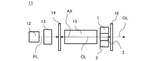
- FIG. 2 is a configuration diagram of a passive Q switch laser device 11 using the passive Q switch element 1.
- the passive Q switch laser device 11 includes a passive Q switch element 1, a semiconductor laser 12, an excitation optical system 13, a total reflection mirror 14, a laser material 15, and an output mirror 16.
- AX indicates the propagation direction axis of the laser beam (the same applies hereinafter).
- the semiconductor laser 12 is an excitation light source for the laser material 15, and the total reflection mirror 14 and the output mirror 16 constitute a spatial resonator.
- AX represents the propagation direction axis of the laser beam.
- the pumping light PL is output from the semiconductor laser 12, and the pumping light PL is shaped by the pumping optical system 13 to become parallel light in the laser material 15, passes through the total reflection mirror 14, and enters the laser material 15.
- the laser material 15 is excited by the excitation light PL, and spontaneous emission light is generated. A part of the light is reciprocated between the total reflection mirror 14 and the output mirror 16, and is amplified each time it passes through the laser material 15.
- the saturable absorber 2 When oscillating, the saturable absorber 2 becomes transparent by absorbing the laser light, so that the loss is reduced, and low-order mode Q-switch pulse light is efficiently generated, and a part of the light is output as the oscillation light OL. 16 is taken out.
- the total reflection mirror 14 and the output mirror 16 can be miniaturized by providing a dielectric film on the end face of the laser material 15 and the end face of the passive Q switch element 1 and integrating them.
- the transparent material 3 has a circular shape (disc shape), but the transparent material has a quadrangular shape (cube: the shape of the cross section perpendicular to the laser light propagation direction is a quadrangle, the same applies hereinafter), and the saturable absorber 2 is bonded to the periphery thereof. It may be. This is effective when the horizontal and vertical directions of the beam can be separated by making the shape of a cube.
- the ring-shaped saturable absorber 2 is optically bonded on the circumference of the disk-shaped transparent material 3.
- the passive Q switch element 1 has a mode selection function so that an efficient low-order mode Q switch pulse light can be obtained without changing the size of the laser device. Can do.
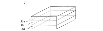
- FIG. FIG. 3 is a block diagram showing a planar waveguide passive Q switch element 21 according to Embodiment 2 of the present invention.
- a planar waveguide passive Q switch element 21 includes a planar saturable absorber 22a (for example, a rectangular plate shape that is flat along the propagation direction of laser light; A second saturable absorber 22b and a planar transparent material 23 are included.
- the first saturable absorber 22a and the second saturable absorber 22b are optically bonded to two opposing surfaces (main surface, hereinafter the same) of the transparent material 23, and the first saturable absorber 22a.
- the second saturable absorber 22b facing the surface bonded to the transparent material 23 (outer main surface) facing the surface bonded to the transparent material 23 of the second saturable absorber 22b. And form a waveguide.
- the transparent material 23 has a coefficient of thermal expansion of the first saturable absorber 22 a and the second saturable absorber 22 b in order to suppress cracking due to stress during bonding.
- a material having an approximately equal or equal coefficient of thermal expansion is used.
- the refractive index of the transparent material 23 is such that the first saturable absorber 22a and the second saturable absorber 22a have a refractive index in order to suppress reflection at the interface between the first saturable absorber 22a and the second saturable absorber 22b.
- a material having a refractive index lower than that of the saturable absorber 22b is used.
- the transparent material 23 has a refractive index (about 1.83), It is advisable to use additive-free YAG having a close thermal expansion coefficient (about 7.8 ⁇ 10 ⁇ 6 / K).
- Co Spinel is used for the first saturable absorber 22a and the second saturable absorber 22b, the transparent material 23 has a refractive index (about 1.70) and a thermal expansion coefficient (about 7. 45 ⁇ 10 ⁇ 6 / K) additive-free Spinel is preferably used.
- the transparent material 23 has a refractive index (about 2.49) and a thermal expansion coefficient.
- additive-free ZnS having a refractive index (about 2.29) and a thermal expansion coefficient (about 6.5 ⁇ 10 ⁇ 6 / K) may be used.
- the first saturable absorber 22a, the second saturable absorber 22b, and the transparent material 23 are optically connected.
- the first saturable absorber 22a, the second saturable absorber, and the like There is a method in which the body 22b and the transparent material 23 are integrally sintered with a ceramic material.
- the first saturable absorber 22a, the second saturable absorber 22b, and the transparent material 23 are joined together by diffusion joining.
- the first saturable absorber 22a, the second saturable absorber 22b, and the transparent material 23 are joined together by surface activation joining.
- first saturable absorber 22a, the second saturable absorber 22b, and the transparent material 23 are integrally joined by optical contact. Furthermore, there is a method in which the first saturable absorber 22a, the second saturable absorber 22b, and the transparent material 23 are integrally bonded with an optical adhesive.
- FIG. 4 is a configuration diagram of a planar waveguide passive Q-switch laser device 31 using the planar waveguide passive Q-switch element 21.
- a planar waveguide passive Q switch laser device 31 includes a planar waveguide passive Q switch element 21, a planar waveguide semiconductor laser 32, an excitation optical system 33, a total reflection mirror 34, and a laser material. 35 and an output mirror 36.
- the semiconductor laser 32 is an excitation light source of the laser material 35, and the total reflection mirror 34 and the output mirror 36 constitute a planar waveguide type resonator.
- the pumping light PL is output from the semiconductor laser 32, and the pumping optical system 33 causes the planar waveguide laser material 35 to have no loss in the vertical direction of the waveguide and to be parallel light in the horizontal direction of the waveguide. Then, the excitation light PL is shaped, passes through the total reflection mirror 34, and enters the planar waveguide laser material 35. The planar waveguide laser material 35 is excited by the excitation light PL, and spontaneous emission light is generated. A part of it is reciprocated between the total reflection mirror 34 and the output mirror 36, and passes through the planar waveguide laser material 35. Amplified every time.
- the gain becomes higher than the intracavity loss including the loss due to the absorption of the first saturable absorber 22a and the second saturable absorber 22b laser oscillation starts in the resonator.
- the resonant light CL is supplied by the planar waveguide type passive Q switch element 21 to the first saturable absorber 22 a provided outside the waveguide of the planar waveguide type passive Q switch element 21.
- the component propagating through the second saturable absorber 22b is absorbed, and the component propagating through the transparent material 23 provided in the central portion of the passive Q switch element 21 is transmitted without loss. It becomes larger and only the low-order mode oscillates.
- the first saturable absorber 22a and the second saturable absorber 22b become transparent by absorbing the laser beam, so that the loss is reduced, and the Q-switch pulse light in the low-order mode is efficiently generated, A part of the light is extracted from the output mirror 36 as the oscillation light OL.
- the total reflection mirror 34 and the output mirror 36 are provided with a dielectric film on the end face of the planar waveguide laser material 35 and the end face of the planar waveguide passive Q switch element 21, respectively, so that the size of the apparatus can be reduced. I can plan.
- the first saturable absorber 22a and the second saturable absorption are formed on the two opposing surfaces of the transparent material 23.
- the body 22b is optically bonded to each other, the surface (outer principal surface) facing the surface bonded to the transparent material 23 of the first saturable absorber 22a, and the transparent of the second saturable absorber 22b. Since the waveguide is formed by the surface (outer principal surface) opposite to the surface bonded to the material 23, the planar waveguide passive Q switch element 21 has a mode other than the original Q switch function. By providing a selection function, it is possible to obtain an efficient low-order mode Q-switched pulse light without changing the size of the laser device. Further, the mode can be controlled even in a waveguide that cannot be mode-controlled spatially.
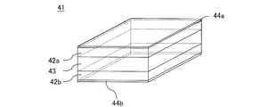
- FIG. 5 is a block diagram showing a planar waveguide passive Q switch element 41 according to the third embodiment of the present invention.
- a planar waveguide passive Q switch element 41 includes a planar first saturable absorber 42a, a planar second saturable absorber 42b, a planar transparent material 43, and a first transparent material 43.
- the first saturable absorber 42a and the second saturable absorber 42b are optically bonded to two opposing surfaces of the transparent material 43, respectively, and bonded to the transparent material 43 of the first saturable absorber 42a.
- the first clad film 44a is provided on the surface facing the surface
- the second clad film 44b is provided on the surface facing the surface bonded to the transparent material 43 of the second saturable absorber 42b.
- the first saturable absorber 42a is bonded to the surface (outer principal surface) facing the surface bonded to the transparent material 43 and the transparent material 43 of the second saturable absorber 42b.
- a waveguide is formed by the surface (outer principal surface) facing the surface.
- the transparent material 43 has a coefficient of thermal expansion of the first saturable absorber 42a and the second saturable absorber 42b in order to suppress cracking due to stress during bonding.
- a material having an approximately equal or equal coefficient of thermal expansion is used.
- the refractive index of the transparent material 43 is such that the first saturable absorber 42a and the second saturable absorber 42a have a refractive index in order to suppress reflection at the interface with the first saturable absorber 42a and the second saturable absorber 42b.
- a material having a refractive index lower than that of the saturable absorber 42b is used, and the first clad film 44a and the second clad film 44b are refracted by the first saturable absorber 42a and the second saturable absorber 42b, respectively.
- a material having a lower refractive index than the refractive index is used.
- the transparent material 43 has a refractive index (about 1.83)
- Additive-free YAG which has a thermal expansion coefficient (about 7.8 ⁇ 10 ⁇ 6 / K)
- SiO 2 reffractive index: about 1.405
- Al 2 O. 3 reffractive index of about 1.61
- M 2 reffractive index of about 1.62
- M 3 refractive index of about 1.74
- Y 2 O 3 refractive index of about 1.81
- the transparent material 43 has a refractive index (about 1.70) and a thermal expansion coefficient (about 7. 45 ⁇ 10 ⁇ 6 / K) additive-free spinel
- the first clad film 44a and the second clad film 44b are made of SiO 2 (refractive index of about 1.45) or Al 2 O 3 (refractive index of about 1.61). ) Or M 2 (refractive index of about 1.62) may be used.
- the transparent material 43 has a refractive index (about 2.49) and a thermal expansion coefficient.
- the first saturable absorber 42a, and the second saturable absorber 42b 43 is an additive-free ZnS having a refractive index (about 2.29) and a thermal expansion coefficient (about 6.5 ⁇ 10 ⁇ 6 / K), and the first cladding film 44a and the second cladding film 44b are made of SiO 2 ( Refractive index about 1.45), Al 2 O 3 (refractive index about 1.61), M 2 (refractive index about 1.62), M 3 (refractive index about 1.74), Y 2 O 3 (refractive index). About 1.81), HfO 3 (refractive index of about 1.90) or Ta 2 O 5 (refractive index of about 2.09) may be used.
- the 1st saturable absorber 42a, the 2nd saturable absorber 42b, and the transparent material 43 are optically connected, for example, the 1st saturable absorber 42a, the 2nd saturable absorber.
- the body 42b and the transparent material 43 are integrally sintered with a ceramic material.
- the first saturable absorber 42a, the second saturable absorber 42b, and the transparent material 43 are joined together by diffusion joining.
- the first saturable absorber 42a, the second saturable absorber 42b, and the transparent material 43 are joined together by surface activation joining.
- first saturable absorber 42a, the second saturable absorber 42b, and the transparent material 43 are integrally joined by optical contact. Furthermore, there is a method in which the first saturable absorber 42a, the second saturable absorber 42b, and the transparent material 43 are integrally bonded with an optical adhesive.
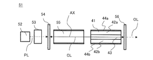
- FIG. 6 is a configuration diagram of a planar waveguide passive Q switch laser device 51 using the planar waveguide passive Q switch element 41.
- a planar waveguide passive Q switch laser device 51 includes a planar waveguide passive Q switch element 41, a semiconductor laser 52, an excitation optical system 53, a total reflection mirror 54, and a planar waveguide laser material 55. And an output mirror 56.
- the semiconductor laser 52 is an excitation light source for the laser material 55, and the total reflection mirror 54 and the output mirror 56 constitute a planar waveguide resonator.
- the pumping light PL is output from the semiconductor laser 52, and the pumping optical system 53 causes the planar waveguide laser material 55 to be parallel light in the horizontal direction of the waveguide without loss in the vertical direction of the waveguide. Then, the excitation light PL is shaped, passes through the total reflection mirror 54, and enters the planar waveguide laser material 55. The planar waveguide laser material 55 is excited by the excitation light PL to generate spontaneously emitted light, part of which reciprocates between the total reflection mirror 54 and the output mirror 56 and passes through the planar waveguide laser material 55. Amplified every time.
- the first saturable absorber 42a and the second saturable absorber 42b become transparent by absorbing the laser light, so that the loss is reduced, and the low-order mode Q switch pulse light is efficiently generated, Part of the light is extracted from the output mirror 56 as the oscillation light OL.
- the total reflection mirror 54 and the output mirror 56 are each provided with a dielectric film on the end face of the planar waveguide type laser material 55 and the end face of the planar waveguide type passive Q switch element 41, so that the size of the apparatus can be reduced. I can plan.
- FIG. 7 shows a simulation result by BPM (beam propagation method).
- the transparent material 43 is additive-free YAG (refractive index 1.813) having a thickness of 100 ⁇ m
- the first clad film 44a and the second clad film 44b have a beam diameter of 200 ⁇ m in order to assume high-order mode light in a waveguide composed of 0.4 ⁇ m thick Al 2 O 3 (refractive index 1.613).
- the intensity distribution before and after transmission when a top-hat shaped beam is incident is shown.
- (b) shows the intensity distribution before and after transmission when a Gaussian beam having a beam diameter of 200 ⁇ m (1 / e 2 ) is incident on the waveguide assuming low-order mode light.
- the transmittance is estimated to be 0.33, whereas when the incident beam has a Gaussian shape (in the case of (b)), it is transmitted.
- the rate was estimated to be 0.69, and it was found that the loss was higher in the higher-order mode light.
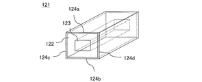
- the vertical direction of the resonant light CL propagates in the waveguide, and the horizontal direction propagates in the radiation mode. It has been described that the lower mode can be achieved by providing the saturable absorbers (42a, 42b) in the vertical direction. However, the saturable absorber as in the ridge waveguide type Q switch element 121 shown in FIG. By providing 122 and the cladding films 124a to 124d over the entire circumference of the laser beam propagation direction axis of the laser material 123 corresponding to the transparent material, the lower-order mode can also be reduced in the horizontal direction.
- a saturable absorber or a cladding film is provided.
- the saturable absorber and the clad film may have any shape such as a combination of planar shapes and a ring shape.
- the first saturable absorber 42a and the second saturable absorption are formed on the two opposing surfaces of the transparent material 43.
- the body 42b is optically bonded to each other, the surface (outside main surface) facing the surface bonded to the transparent material 43 of the first saturable absorber 42a, and the transparent of the second saturable absorber 42b. Since the waveguide is formed by the surface (outer principal surface) opposite to the surface bonded to the material 43, the passive Q switch element 41 has a mode selection function in addition to the original Q switch function. Thus, it is possible to obtain an efficient low-order mode Q-switched pulse light without changing the size of the laser device. Further, the mode can be controlled even in a waveguide that cannot be mode-controlled spatially.
- FIG. FIG. 8 is a block diagram showing a passive Q switch element 61 according to Embodiment 4 of the present invention.
- the passive Q switch element 61 includes a ring-shaped saturable absorber 62 and a disk-shaped laser material 63, and the saturable absorber 62 is optically bonded on the circumference of the laser material 63. Yes.
- the passive Q switch element 61 a material in which the refractive index and the thermal expansion coefficient of the saturable absorber 62 and the laser material 63 are approximately the same or equal is used. If the refractive index difference between the saturable absorber 62 and the laser material 63 is large, the loss due to wavefront aberration increases, so a smaller one is desirable. In order to set the wavefront aberration to ⁇ / 4 or less (wavefront aberration loss 0.012) in the pv value, assuming that the wavelength is 1064 nm and the thickness of the passive Q switch element 61 is 1 mm, the saturable absorber 62 and the laser material The refractive index difference of 63 is
- ⁇ RMS Wavefront aberration
- ⁇ n Refractive index difference
- L Thickness of the passive Q switch element 61
- ⁇ Wavelength.
- the saturable absorber 62 has a refractive index (about 1.83) which is used as a passive Q switch material in the 0.9 to 1.3 ⁇ m band.
- Cr 4+ : YAG or V 3+ : YAG having a close thermal expansion coefficient (about 7.8 ⁇ 10 ⁇ 6 / K) may be used.
- the saturable absorber 62 and the laser material 63 are optically connected.
- the saturable absorber 62 and the laser material 63 are integrally sintered with a ceramic material.
- the saturable absorber 62 and the laser material 63 are joined together by diffusion joining.
- the saturable absorber 62 and the laser material 63 are bonded together by surface activated bonding.
- the saturable absorber 62 and the laser material 63 are joined together by optical contact.
- the saturable absorber 62 and the laser material 63 are bonded together with an optical adhesive.
- FIG. 9 is a block diagram of a passive Q switch laser device 71 using a passive Q switch element 61.
- the passive Q switch laser device 71 includes a passive Q switch element 61, a semiconductor laser 72, an excitation optical system 73, a total reflection mirror 74, and an output mirror 75.
- the semiconductor laser 72 is an excitation light source for the laser material 63 in the passive Q switch element 61, and the total reflection mirror 74 and the output mirror 75 constitute a spatial resonator.
- Excitation light PL is output from the semiconductor laser 72, and the excitation light PL is shaped by the excitation optical system 73 so as to become parallel light in the laser material 63 in the passive Q switch element 61, passes through the total reflection mirror 74, The light enters the laser material 63 in the passive Q switch element 61.
- the laser material 63 in the passive Q switch element 61 is excited by the excitation light PL and spontaneous emission light is generated.
- a part of the laser material 63 reciprocates between the total reflection mirror 74 and the output mirror 75, Each time it passes through the laser material 63, it is amplified.
- the total reflection mirror 74 and the output mirror 75 are each provided with a dielectric film on the end face of the passive Q switch element 61, and can be miniaturized by integrating them.
- the laser material 63 has a circular shape (disc shape), but the laser material has a quadrangular shape (cube: a cross-sectional shape perpendicular to the propagation direction of the laser beam is a quadrangle, the same applies hereinafter), and a saturable absorber is bonded to the periphery thereof. May be. It becomes effective when the horizontal direction and the vertical direction of the beam can be separated by making the shape a cube.
- the ring-shaped saturable absorber 62 is optically bonded on the circumference of the disk-shaped laser material 63.
- the passive Q switch element 61 has a mode selection function in addition to the original Q switch function, so that an efficient low-order mode Q switch pulse light can be obtained without changing the size of the laser device. Can do. .
- the laser device can be miniaturized.
- FIG. FIG. 10 is a block diagram showing a planar waveguide passive Q switch element 81 according to the fifth embodiment of the present invention.
- the planar waveguide passive Q switch element 81 includes a planar first saturable absorber 82 a, a planar second saturable absorber 82 b, and a planar laser material 83. Is done.
- the first saturable absorber 82a and the second saturable absorber 82b are optically bonded to two opposing surfaces of the laser material 83, respectively, and bonded to the laser material 83 of the first saturable absorber 82a.
- a waveguide is formed by a surface (outer main surface) opposite to the surface being connected and a surface (outer main surface) facing the surface joined to the laser material 83 of the second saturable absorber 82b.
- the laser material 83 has a coefficient of thermal expansion of the first saturable absorber 82a and the second saturable absorber 82b in order to suppress cracking due to stress during bonding. Use approximately equal or equal materials.
- the refractive index of the laser material 83 is such that the first saturable absorber 82a and the second saturable absorber 82a have a refractive index in order to suppress reflection at the interface with the first saturable absorber 82a and the second saturable absorber 82b.
- a material having a refractive index lower than that of the saturable absorber 82b is used.
- the first saturable absorber 82a and the second saturable absorber 82b have a passive Q switch in the 0.9 to 1.3 ⁇ m band.
- Cr 4+ : YAG or V 3+ : YAG which are used as materials and have a refractive index (about 1.83) and a thermal expansion coefficient (about 7.8 ⁇ 10 ⁇ 6 / K), are preferably used.
- Er glass (refractive index of 1.53) is used for the laser material 83
- the first saturable absorber 82a and the second saturable absorber 82b are used as eye-safe band passive Q switch materials.
- Co Spinel having a refractive index (about 1.70) and a thermal expansion coefficient (about 7.45 ⁇ 10 ⁇ 6 / K), a refractive index (about 2.49), a thermal expansion coefficient (about 7.6 ⁇ 10 -6 / K) Co2 +: ZnSe or Cr2 +: ZnSe, Co2 + having a refractive index (about 2.29) and a coefficient of thermal expansion (about 6.5 ⁇ 10 -6 / K): ZnS or Cr2 +: ZnS are used. Good.
- the first saturable absorber 82a and the second saturable absorber 82b are used as eye-safe band passive Q switch materials.
- 6.5 ⁇ 10 ⁇ 6 / K) of Co 2+: ZnS or Cr 2+: ZnS may be used.
- the first saturable absorber 82a and the second saturable absorber 82b have eye-safety.
- Co2 +: ZnS or Cr2 +: ZnS having a coefficient of thermal expansion (about 6.5 ⁇ 10 ⁇ 6 / K) may be used.
- first saturable absorber 82a, the second saturable absorber 82b, and the laser material 83 are optically connected.
- first saturable absorber 82a, the second saturable absorber 82a, and the second saturable absorber 82a There is a method in which the body 82b and the laser material 83 are integrally sintered with a ceramic material. Further, there is a method in which the first saturable absorber 82a, the second saturable absorber 82b, and the laser material 83 are integrally joined by diffusion joining.
- first saturable absorber 82a, the second saturable absorber 82b, and the laser material 83 are integrally bonded by surface activated bonding. Further, there is a method in which the first saturable absorber 82a, the second saturable absorber 82b, and the laser material 83 are integrally joined by optical contact. Further, there is a method in which the first saturable absorber 82a, the second saturable absorber 82b, and the laser material 83 are integrally bonded with an optical adhesive.
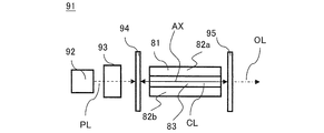
- FIG. 11 is a configuration diagram of a planar waveguide passive Q-switch laser device 91 using a planar waveguide passive Q-switch element 81.
- a planar waveguide passive Q switch laser device 91 includes a planar waveguide passive Q switch element 81, a planar waveguide semiconductor laser 92, an excitation optical system 93, a total reflection mirror 94, and an output mirror. 95.
- the semiconductor laser 92 is an excitation light source of the laser material 83 in the passive Q switch element 81, and the total reflection mirror 94 and the output mirror 95 constitute a planar waveguide type resonator.
- the pumping light PL is output from the semiconductor laser 92, and the pumping optical system 93 causes no loss in the planar waveguide passive Q switch element 81 in the vertical direction of the waveguide, and parallel light in the horizontal direction of the waveguide.
- the excitation light PL is shaped, passes through the total reflection mirror 94, and enters the planar waveguide passive Q switch element 81.
- the laser material 83 in the planar waveguide passive Q switch element 81 is excited by the excitation light PL, and spontaneous emission light is generated. A part of the laser material 83 reciprocates between the total reflection mirror 94 and the output mirror 95, and the planar waveguide Each time it passes through the laser material 83 in the type passive Q switch element 81, it is amplified.
- the first saturable absorber 82a and the second saturable absorber 82b become transparent by absorbing the laser light, so that the loss is reduced and the Q-switch pulse light in the lower order mode is efficiently generated. , A part of the light is extracted from the output mirror 95 as the oscillation light OL.
- the total reflection mirror 94 and the output mirror 95 can be reduced in size by providing a dielectric film on both end faces of the planar waveguide passive Q switch element 81 and integrating them.
- the first saturable absorber 82a and the second saturable absorption are provided on the two opposing surfaces of the laser material 83.
- the body 82b is optically bonded to each other, the surface (outer main surface) facing the surface bonded to the laser material 83 of the first saturable absorber 82a, and the laser of the second saturable absorber 82b. Since the waveguide is formed by the surface (outer principal surface) opposite to the surface bonded to the material 83, the planar waveguide passive Q switch element 81 has a mode selection function in addition to the original Q switch function.
- the mode can be controlled even in a waveguide where the mode cannot be spatially controlled.
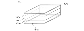
- FIG. 12 is a block diagram showing a planar waveguide passive Q switch element 101 according to the sixth embodiment of the present invention.
- a planar waveguide passive Q switch element 101 includes a planar first saturable absorber 102a, a planar second saturable absorber 102b, a planar laser material 103, a first The clad film 104a and the second clad film 104b.
- the first saturable absorber 102a and the second saturable absorber 102b are optically bonded to two opposing surfaces of the laser material 103, respectively, and bonded to the laser material 103 of the first saturable absorber 102a.
- the first clad film 104a is provided on the surface facing the surface of the second saturable absorber 102b
- the second clad film 104b is provided on the surface of the second saturable absorber 102b facing the surface bonded to the laser material 103.
- the first saturable absorber 102a is bonded to the laser material 103 of the second saturable absorber 102b and the surface (outer main surface) opposite to the surface bonded to the laser material 103 of the first saturable absorber 102a.
- a waveguide is formed by the surface (outer principal surface) facing the surface.
- the laser material 103 has a coefficient of thermal expansion of the first saturable absorber 102a and the second saturable absorber 102b in order to suppress cracking due to stress during bonding.
- a material having an approximately equal or equal coefficient of thermal expansion is used.
- the refractive index of the laser material 103 is such that the first saturable absorber 102a and the second saturable absorber 102a have a refractive index in order to suppress reflection at the interface with the first saturable absorber 102a and the second saturable absorber 102b.
- a material having a refractive index lower than that of the saturable absorber 102b is used.
- the first clad film 104a and the second clad film 104b are made of a material having a refractive index lower than that of the first saturable absorber 102a and the second saturable absorber 102b, respectively.
- the first saturable absorber 102a and the second saturable absorber 102b have a passive Q switch in the 0.9 to 1.3 ⁇ m band.
- the second cladding film 104b is made of SiO 2 (refractive index of about 1.45), Al 2 O 3 (refractive index of about 1.61), M 2 (refractive index of about 1.62), M 3 (refractive index of about 1). .74) or Y 2 O 3 (refractive index of about 1.81) may be used.
- SiO 2 reffractive index of about 1.45
- Al 2 O 3 reffractive index of about 1.61
- M 2 reffractive index of about 1.62
- M 3 refractive index of about 1). .74
- Y 2 O 3 refractive index of about 1.81
- Er glass (refractive index of 1.53)
- the first saturable absorber 102a and the second saturable absorber 102b are used as passive Q switch materials in the eye-safe band.
- Co Spinel having a refractive index (about 1.70) and a thermal expansion coefficient (about 7.45 ⁇ 10 ⁇ 6 / K), a refractive index (about 2.49), a thermal expansion coefficient (about 7.6 ⁇ 10 -6 / K) Co2 +: ZnSe or Cr2 +: ZnSe, Co2 + having a refractive index (about 2.29) and a coefficient of thermal expansion (about 6.5 ⁇ 10 -6 / K): ZnS or Cr2 +: ZnS are used.
- the first saturable absorber 102a and the second saturable absorber 102b are made of Co: Spinel, the first cladding film 104a and the second cladding film 104b are made of SiO 2 (with a refractive index of about 1.45), Al 2 O 3 (refractive index of about 1.61), M 2 (refractive index of about 1.62). ) Is recommended.
- the clad film 104b is made of SiO 2 (refractive index of about 1.45), Al 2 O 3 (refractive index of about 1.61), M 2 (refractive index of about 1.62), M 3 (refractive index of about 1.74), Y 2 O 3 (refractive index of about 1.81), HfO 3 (refractive index of about 1.90), or Ta 2 O 5 (refractive index of about 2.09) may be used.
- first saturable absorber 102a, the second saturable absorber 102b, and the laser material 103 are optically connected.
- first saturable absorber 102a, the second saturable absorber 102, and the second saturable absorber 102b There is a method in which the body 102b and the laser material 103 are integrally sintered with a ceramic material.
- first saturable absorber 102a, the second saturable absorber 102b, and the laser material 103 are integrally bonded by diffusion bonding.
- first saturable absorber 102a, the second saturable absorber 102b, and the laser material 103 are bonded together by surface activation bonding. Further, there is a method in which the first saturable absorber 102a, the second saturable absorber 102b, and the laser material 103 are integrally joined by optical contact. Further, there is a method in which the first saturable absorber 102a, the second saturable absorber 102b, and the laser material 103 are integrally bonded with an optical adhesive.
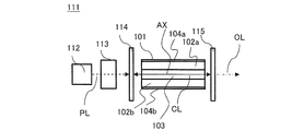
- FIG. 13 is a configuration diagram of a planar waveguide passive Q switch laser device 111 using the planar waveguide passive Q switch element 101.
- the planar waveguide passive Q switch laser device 111 includes a planar waveguide passive Q switch element 101, a semiconductor laser 112, an excitation optical system 113, a total reflection mirror 114, and an output mirror 115.
- the semiconductor laser 112 is an excitation light source for the laser material 103 in the passive Q switch element 101, and the total reflection mirror 114 and the output mirror 115 constitute a planar waveguide resonator.
- the pumping light PL is output from the semiconductor laser 112, and the pumping optical system 113 causes the planar waveguide passive Q switch element 101 to have no loss in the vertical direction of the waveguide and parallel light in the horizontal direction of the waveguide.
- the excitation light PL is shaped so that it passes through the total reflection mirror 114 and enters the planar waveguide type passive Q switch element 101.
- the laser material 103 in the planar waveguide passive Q switch element 101 is excited by the excitation light PL, and spontaneous emission light is generated. A part of the laser material 103 reciprocates between the total reflection mirror 114 and the output mirror 115, and the planar waveguide Each time it passes through the laser material 103 in the type passive Q switch element 101, it is amplified.
- the first saturable absorber 102a and the second saturable absorber 102b become transparent by absorbing the laser light, so that the loss is reduced and the Q-switch pulse light in the low-order mode is efficiently generated. A part of the light is extracted from the output mirror 115 as the oscillation light OL.
- the total reflection mirror 114 and the output mirror 115 are each provided with a dielectric film on both end faces of the planar waveguide type passive Q switch element 101, and can be miniaturized by integrating them.
- FIG. 14 is a block diagram showing a ridge waveguide passive Q switch element 121 according to the seventh embodiment of the present invention.
- a ridge waveguide passive Q switch element 121 includes a cubic saturable absorber 122 having a hollow center, a cubic laser material or transparent material 123, a first cladding film 124a, The second clad film 124b, the third clad film 124c, and the fourth clad film 124d.
- the saturable absorber 122 is optically bonded to all surfaces parallel to the optical axis of the laser material 123, and on the surface facing the surface bonded to the laser material 123 of the saturable absorber 122, First to fourth clad films 124a to 124d are provided, and a waveguide is formed by the saturable absorber 122 and a surface (outer principal surface) facing the surface bonded to the laser material 123.
- the laser material 123 uses a material having a thermal expansion coefficient substantially equal to or equal to the thermal expansion coefficient of the saturable absorber 122 in order to suppress cracking due to stress during bonding.
- a material whose refractive index is lower than that of the saturable absorber 122 is used in order to suppress reflection at the interface with the saturable absorber 122.
- the first to fourth clad films 124 a to 124 d are made of a material having a refractive index lower than that of the saturable absorber 122.
- the saturable absorber 122 is used as a passive Q-switch material in the 0.9 to 1.3 ⁇ m band and has a refractive index (about 1.83).
- Cr 4+ : YAG or V 3+ : YAG having a thermal expansion coefficient (about 7.8 ⁇ 10 ⁇ 6 / K) is used, and the first to fourth cladding films 124a to 124d are made of SiO 2 ( Refractive index about 1.45), Al 2 O 3 (refractive index about 1.61), M 2 (refractive index about 1.62), M 3 (refractive index about 1.74), Y 2 O 3 (refractive index).
- the saturable absorber 122 has a refractive index (about 1.70), heat, which is used as a passive Q switch material in the eye-safe band.
- Co of expansion (about 7.45 ⁇ 10 -6 / K): Spinel and a refractive index (about 2.49), the thermal expansion coefficient (about 7.6 ⁇ 10 -6 / K) Co2 +: ZnSe or Cr2 + : ZnSe or Co2 +: ZnS or Cr2 +: ZnS having a refractive index (about 2.29) and a thermal expansion coefficient (about 6.5 ⁇ 10 ⁇ 6 / K) may be used, and the saturable absorber 122 may be made of Co: Spinel.
- the first to fourth clad films 124a to 124d are made of SiO 2 (refractive index of about 1.45), Al 2 O 3 (refractive index of about 1.61), M 2 (refractive index of about 1). .62) may be used.
- the first to fourth cladding films 124a to 124d have SiO 2 (refractive index of about 1.
- Al 2 O 3 (refractive index of about 1.61), M 2 (refractive index of about 1.62), M 3 (refractive index of about 1.74), Y 2 O 3 (refractive index of about 1.81). HfO 3 (refractive index of about 1.90) or Ta 2 O 5 (refractive index of about 2.09) may be used.
- the saturable absorber 122 and the laser material 123 are optically connected.
- the saturable absorber 122 and the laser material 123 are integrally sintered with a ceramic material.
- the saturable absorber 122 and the laser material 123 are integrally bonded by diffusion bonding.
- the saturable absorber 122 and the laser material 123 are joined together by surface activated joining.
- the saturable absorber 122 and the laser material 123 are joined together by optical contact.
- the saturable absorber 122 and the laser material 123 are bonded together with an optical adhesive.
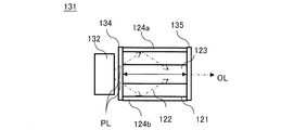
- FIG. 15 is a configuration diagram of a ridge waveguide passive Q switch laser device 131 using a ridge waveguide passive Q switch element 121.
- the ridge waveguide Q-switch laser device 131 includes a ridge waveguide passive Q switch element 121, a semiconductor laser 132, a total reflection film 134, and a partial reflection film 135.
- the partial reflection film 135 constitutes a ridge waveguide type resonator.
- the excitation light PL output from the semiconductor laser 132 passes through the total reflection film 134 and enters the ridge waveguide passive Q switch element 121.
- the pumping light PL output from the semiconductor laser 132 spreads in the vertical direction and the horizontal direction, and the vertical component of the pumping light PL is the first cladding film 124a of the ridge waveguide passive Q switch element 121 and the second clad film 124a. It is confined by the clad film 124b and propagates in the waveguide. Further, the horizontal component of the excitation light PL is confined by the third cladding film 124c and the fourth cladding film 124d of the ridge waveguide passive Q switch element 121 and propagates in the waveguide.
- the laser material 123 in the ridge waveguide passive Q switch element 121 is excited by the excitation light PL, and spontaneous emission light is generated. A part of the laser material 123 reciprocates between the total reflection film 134 and the partial reflection film 135, and the ridge guide Each time it passes through the laser material 123 in the waveguide passive Q switch element 121, it is amplified.
- the saturable absorber 122 When oscillated, the saturable absorber 122 becomes transparent by absorbing the laser light, so that the loss is reduced, and the low-order mode Q-switched pulse light is efficiently generated, and a part of the light is the oscillation light, and the output light OL As shown in FIG.
- the switch element 121 has a saturable absorber 122 inside the first clad film 124a, the second clad film 124b, the third clad film 124c, and the fourth clad film 124d. Light oscillated in the optical path is absorbed by the saturable absorber 121, and parasitic oscillation can be suppressed.
- the saturable absorber 122 is optically applied to all surfaces parallel to the optical axis of the laser material 123. Since the first to fourth clad films 124a to 124d are provided on the surface that is bonded to the surface that is bonded to the laser material 123 of the saturable absorber, the ridge waveguide passive Q switch element 121 includes Since it has a mode selection function in addition to the original Q switch function, it is possible to obtain an efficient low-order mode Q switch pulsed light.
- the laser device since it functions as a laser material, it is possible to reduce the size of the laser device and to suppress the coupling loss that normally occurs between the waveguide laser material and the waveguide Q switch element. Further, the mode can be controlled even in a waveguide where the mode cannot be spatially controlled.
- the cladding is also provided in the horizontal direction and the vertical direction, no excitation optical system is required, and the laser device can be downsized. Furthermore, the parasitic oscillation which is a concern when the pumping light output is increased can be suppressed by the saturable absorber inside the cladding.
- the present invention can be applied to passive Q switch elements, passive Q switch laser devices, and the like in various fields, and has similar effects.
Landscapes
- Physics & Mathematics (AREA)
- Electromagnetism (AREA)
- Nonlinear Science (AREA)
- Optics & Photonics (AREA)
- Engineering & Computer Science (AREA)
- Plasma & Fusion (AREA)
- General Physics & Mathematics (AREA)
- Lasers (AREA)
- Optical Modulation, Optical Deflection, Nonlinear Optics, Optical Demodulation, Optical Logic Elements (AREA)
Abstract
Priority Applications (4)
| Application Number | Priority Date | Filing Date | Title |
|---|---|---|---|
| JP2014514675A JP5734511B2 (ja) | 2012-05-09 | 2013-04-25 | 受動qスイッチ素子 |
| EP13787075.4A EP2849293B1 (fr) | 2012-05-09 | 2013-04-25 | Element a declenchement passif et dispositif laser declenche passivement |
| US14/390,901 US9337609B2 (en) | 2012-05-09 | 2013-04-25 | Passively Q-switched element and passively Q-switched laser device |
| CN201380024084.6A CN104272537B (zh) | 2012-05-09 | 2013-04-25 | 被动q开关元件以及被动q开关激光装置 |
Applications Claiming Priority (2)
| Application Number | Priority Date | Filing Date | Title |
|---|---|---|---|
| JP2012107393 | 2012-05-09 | ||
| JP2012-107393 | 2012-05-09 |
Publications (1)
| Publication Number | Publication Date |
|---|---|
| WO2013168587A1 true WO2013168587A1 (fr) | 2013-11-14 |
Family
ID=49550633
Family Applications (1)
| Application Number | Title | Priority Date | Filing Date |
|---|---|---|---|
| PCT/JP2013/062252 Ceased WO2013168587A1 (fr) | 2012-05-09 | 2013-04-25 | Élément de laser déclenché passif, et dispositif de laser déclenché passif |
Country Status (5)
| Country | Link |
|---|---|
| US (1) | US9337609B2 (fr) |
| EP (1) | EP2849293B1 (fr) |
| JP (1) | JP5734511B2 (fr) |
| CN (1) | CN104272537B (fr) |
| WO (1) | WO2013168587A1 (fr) |
Cited By (6)
| Publication number | Priority date | Publication date | Assignee | Title |
|---|---|---|---|---|
| JP2017112139A (ja) * | 2015-12-14 | 2017-06-22 | 株式会社豊田中央研究所 | レーザ発振装置 |
| JP2021061343A (ja) * | 2019-10-08 | 2021-04-15 | 株式会社Ihi | レーザー出力装置、および、レーザー出力装置の製造方法 |
| JPWO2020144915A1 (ja) * | 2019-01-10 | 2021-09-09 | Jx金属株式会社 | 光吸収層及び光吸収層を備えた接合体 |
| JP2021530116A (ja) * | 2018-06-22 | 2021-11-04 | キャンデラ コーポレイション | キャビティ内コーティングを備えたパッシブqスイッチマイクロチップレーザー、及びそのマイクロチップレーザーを備えたハンドピース |
| JP2022022765A (ja) * | 2020-07-06 | 2022-02-07 | 古河電気工業株式会社 | 結合モジュール及び焼灼装置 |
| US11381053B2 (en) * | 2019-12-18 | 2022-07-05 | Globalfoundries U.S. Inc. | Waveguide-confining layer with gain medium to emit subwavelength lasers, and method to form same |
Families Citing this family (7)
| Publication number | Priority date | Publication date | Assignee | Title |
|---|---|---|---|---|
| IL251520A0 (en) * | 2017-04-02 | 2017-06-29 | Jerusalem College Of Tech | Tolerable inversion of quality factor in a pumped-diode laser |
| EP3680998B1 (fr) * | 2017-09-05 | 2023-06-14 | National Institutes for Quantum Science and Technology | Dispositif laser, source de lumière et dispositif de mesure |
| US12003072B2 (en) | 2019-07-16 | 2024-06-04 | Nichia Corporation | Q switch resonator, and pulse generator |
| CN113056682B (zh) * | 2019-10-24 | 2022-04-29 | 趣眼有限公司 | 光子系统及方法 |
| US12095226B2 (en) | 2019-10-24 | 2024-09-17 | Trieye Ltd. | Passive Q-switched lasers and methods for operation and manufacture thereof |
| WO2021157135A1 (fr) * | 2020-02-07 | 2021-08-12 | Jx金属株式会社 | Corps assemblé en céramique yag et son procédé de production |
| WO2022053924A1 (fr) * | 2020-09-08 | 2022-03-17 | Trieye Ltd. | Laser déclenché passivement innovant |
Citations (8)
| Publication number | Priority date | Publication date | Assignee | Title |
|---|---|---|---|---|
| JPH0626273B2 (ja) | 1987-09-24 | 1994-04-06 | 富士電機株式会社 | レーザ発振装置 |
| JPH07183607A (ja) * | 1993-11-15 | 1995-07-21 | Commiss Energ Atom | 可飽和吸収体により受動スイッチングするレーザーキャビティ及びそのキャビティを有するレーザー |
| WO1995022186A1 (fr) * | 1994-02-08 | 1995-08-17 | Massachusetts Institute Of Technology | Microlaser a commutation q passive a impulsions de l'ordre de la picoseconde |
| JPH1084157A (ja) * | 1996-07-26 | 1998-03-31 | Commiss Energ Atom | モード選択機能付マイクロレーザーキャビティおよびマイクロレーザーならびにその製造方法 |
| JP2980788B2 (ja) | 1992-10-21 | 1999-11-22 | 三菱電機株式会社 | レーザ装置 |
| JP2005327997A (ja) * | 2004-05-17 | 2005-11-24 | Akio Ikesue | 複合レーザー素子及びその素子を用いたレーザー発振器 |
| EP1978611A1 (fr) * | 2007-04-03 | 2008-10-08 | Topcon Corporation | Microlaser à déclenchément et procédé d'utilisation |
| JP2009010066A (ja) * | 2007-06-27 | 2009-01-15 | Covalent Materials Corp | パルスレーザ発振器 |
Family Cites Families (8)
| Publication number | Priority date | Publication date | Assignee | Title |
|---|---|---|---|---|
| US3440562A (en) * | 1964-06-15 | 1969-04-22 | Warner Lambert Pharmaceutical | Bistable laser structure |
| US3626319A (en) * | 1970-04-14 | 1971-12-07 | Warner Lambert Pharmaceutical | Laser structures and the like |
| US5441803A (en) * | 1988-08-30 | 1995-08-15 | Onyx Optics | Composites made from single crystal substances |
| FR2750539B1 (fr) | 1996-06-28 | 1998-07-24 | Commissariat Energie Atomique | Materiaux laser et microlasers a fortes concentrations en ions actifs, et procedes de fabrication |
| GB9625231D0 (en) * | 1996-12-04 | 1997-01-22 | Univ Southampton | Optical amplifiers & lasers |
| US6160824A (en) * | 1998-11-02 | 2000-12-12 | Maxios Laser Corporation | Laser-pumped compound waveguide lasers and amplifiers |
| TW200301980A (en) * | 2002-01-10 | 2003-07-16 | Hrl Lab Llc | Diffusion bonded pump cavity |
| US8194709B2 (en) | 2008-06-11 | 2012-06-05 | Massachusetts Institute Of Technology | High-repetition-rate guided-mode femtosecond laser |
-
2013
- 2013-04-25 US US14/390,901 patent/US9337609B2/en active Active
- 2013-04-25 JP JP2014514675A patent/JP5734511B2/ja active Active
- 2013-04-25 EP EP13787075.4A patent/EP2849293B1/fr active Active
- 2013-04-25 WO PCT/JP2013/062252 patent/WO2013168587A1/fr not_active Ceased
- 2013-04-25 CN CN201380024084.6A patent/CN104272537B/zh active Active
Patent Citations (8)
| Publication number | Priority date | Publication date | Assignee | Title |
|---|---|---|---|---|
| JPH0626273B2 (ja) | 1987-09-24 | 1994-04-06 | 富士電機株式会社 | レーザ発振装置 |
| JP2980788B2 (ja) | 1992-10-21 | 1999-11-22 | 三菱電機株式会社 | レーザ装置 |
| JPH07183607A (ja) * | 1993-11-15 | 1995-07-21 | Commiss Energ Atom | 可飽和吸収体により受動スイッチングするレーザーキャビティ及びそのキャビティを有するレーザー |
| WO1995022186A1 (fr) * | 1994-02-08 | 1995-08-17 | Massachusetts Institute Of Technology | Microlaser a commutation q passive a impulsions de l'ordre de la picoseconde |
| JPH1084157A (ja) * | 1996-07-26 | 1998-03-31 | Commiss Energ Atom | モード選択機能付マイクロレーザーキャビティおよびマイクロレーザーならびにその製造方法 |
| JP2005327997A (ja) * | 2004-05-17 | 2005-11-24 | Akio Ikesue | 複合レーザー素子及びその素子を用いたレーザー発振器 |
| EP1978611A1 (fr) * | 2007-04-03 | 2008-10-08 | Topcon Corporation | Microlaser à déclenchément et procédé d'utilisation |
| JP2009010066A (ja) * | 2007-06-27 | 2009-01-15 | Covalent Materials Corp | パルスレーザ発振器 |
Non-Patent Citations (5)
| Title |
|---|
| DONG JUN ET AL.: "EFFICIENT PASSIVELY Q-SWITCHED YB:LUAG MICROCHIP LASER", OPTICS LETTERS, vol. 32, no. 22, 15 November 2007 (2007-11-15), pages 3266 - 3268, XP001509374 * |
| MACKENZIE J. I. ET AL.: "END-PUMPED, PASSIVELY Q-SWITCHED YB:YAG DOUBLE-CLAD WAVEGUIDE LASER", OPTICS LETTERS, vol. 27, no. 24, 15 December 2002 (2002-12-15), pages 2161 - 2163, XP055169180 * |
| W. KOECHNER: "Solid-State Laser Engineering, Sixth Revised and Updated Edition", 2006, pages: 528 |
| YOSUKE AKINO ET AL.: "LAV-10-24 Passive Q-switched planar waveguide laser using a saturation absorber", THE INSTITUTE OF ELECTRICAL ENGINEERS OF JAPAN KENKYUKAI SHIRYO HIKARI OYO SHIKAKU KENKYUKAI, 27 December 2010 (2010-12-27), pages 1 - 5, XP008175089 * |
| ZAYHOWSKI JOHN J. ET AL.: "PUMP-INDUCED BLEACHING OF THE SATURABLE ABSORBER IN SHORT-PULSE ND:YAG/CR4+:YAG PASSIVELY Q-SWITCHED MICROCHIP LASERS", IEEE JOURNAL OF QUANTUM ELECTRONICS, vol. 39, no. 12, December 2003 (2003-12-01), pages 1588 - 1593, XP011104364 * |
Cited By (8)
| Publication number | Priority date | Publication date | Assignee | Title |
|---|---|---|---|---|
| JP2017112139A (ja) * | 2015-12-14 | 2017-06-22 | 株式会社豊田中央研究所 | レーザ発振装置 |
| JP2021530116A (ja) * | 2018-06-22 | 2021-11-04 | キャンデラ コーポレイション | キャビティ内コーティングを備えたパッシブqスイッチマイクロチップレーザー、及びそのマイクロチップレーザーを備えたハンドピース |
| JP2024063207A (ja) * | 2018-06-22 | 2024-05-10 | キャンデラ コーポレイション | キャビティ内コーティングを備えたパッシブqスイッチマイクロチップレーザー、及びそのマイクロチップレーザーを備えたハンドピース |
| JPWO2020144915A1 (ja) * | 2019-01-10 | 2021-09-09 | Jx金属株式会社 | 光吸収層及び光吸収層を備えた接合体 |
| JP7052088B2 (ja) | 2019-01-10 | 2022-04-11 | Jx金属株式会社 | 光吸収層及び光吸収層を備えた接合体 |
| JP2021061343A (ja) * | 2019-10-08 | 2021-04-15 | 株式会社Ihi | レーザー出力装置、および、レーザー出力装置の製造方法 |
| US11381053B2 (en) * | 2019-12-18 | 2022-07-05 | Globalfoundries U.S. Inc. | Waveguide-confining layer with gain medium to emit subwavelength lasers, and method to form same |
| JP2022022765A (ja) * | 2020-07-06 | 2022-02-07 | 古河電気工業株式会社 | 結合モジュール及び焼灼装置 |
Also Published As
| Publication number | Publication date |
|---|---|
| CN104272537B (zh) | 2017-08-08 |
| EP2849293B1 (fr) | 2019-06-12 |
| JPWO2013168587A1 (ja) | 2016-01-07 |
| EP2849293A4 (fr) | 2016-06-29 |
| US9337609B2 (en) | 2016-05-10 |
| EP2849293A1 (fr) | 2015-03-18 |
| JP5734511B2 (ja) | 2015-06-17 |
| US20150117476A1 (en) | 2015-04-30 |
| CN104272537A (zh) | 2015-01-07 |
Similar Documents
| Publication | Publication Date | Title |
|---|---|---|
| JP5734511B2 (ja) | 受動qスイッチ素子 | |
| JP4754020B2 (ja) | 平面導波路型レーザ装置 | |
| US5256164A (en) | Method of fabricating a microchip laser | |
| TWI430527B (zh) | Q-切換引發之增益切換鉺脈衝雷射系統 | |
| JP6253672B2 (ja) | 平面導波路型レーザ装置 | |
| JP6632644B2 (ja) | 光学素子の製造方法及び光学素子 | |
| CN110741516B (zh) | 无源q开关脉冲激光装置、处理设备和医疗设备 | |
| US5732100A (en) | Cavity for a solid microlaser having an optimized efficiency, microlaser using it and its production process | |
| CN100437167C (zh) | 外部谐振器和利用其的半导体激光模块 | |
| JP2007036195A (ja) | 多重光路の固体スラブレーザロッドまたは非線形光学結晶を用いたレーザ装置 | |
| JPH11261136A (ja) | 光パルス発生素子 | |
| JPH06308553A (ja) | 光波長変換装置 | |
| US7085303B2 (en) | Laser with combined lens and birefringence compensator | |
| US8223813B2 (en) | Semiconductor laser pumped solid-state laser device | |
| US10985521B2 (en) | Ridge waveguide laser device | |
| JP7511902B2 (ja) | レーザ加工装置及びレーザ加工方法 | |
| JP6690869B2 (ja) | 平面導波路及びレーザ増幅器 | |
| JPWO2006098313A1 (ja) | 光増幅器およびレーザ装置 | |
| WO2023080242A1 (fr) | Élément optique, dispositif optique et procédé de production d'élément optique | |
| WO2021171957A1 (fr) | Résonateur optique, composant pour résonateur optique et dispositif laser | |
| CN114696194A (zh) | 可插入式单块非平面环形腔激光装置 | |
| Kudryashov et al. | Laser Resonators, Microresonators, and Beam Control XIX | |
| JPH1074994A (ja) | 固体レーザ装置 |
Legal Events
| Date | Code | Title | Description |
|---|---|---|---|
| 121 | Ep: the epo has been informed by wipo that ep was designated in this application |
Ref document number: 13787075 Country of ref document: EP Kind code of ref document: A1 |
|
| ENP | Entry into the national phase |
Ref document number: 2014514675 Country of ref document: JP Kind code of ref document: A |
|
| WWE | Wipo information: entry into national phase |
Ref document number: 14390901 Country of ref document: US |
|
| WWE | Wipo information: entry into national phase |
Ref document number: 2013787075 Country of ref document: EP |
|
| NENP | Non-entry into the national phase |
Ref country code: DE |