EP1983614A1 - Module à haute fréquence - Google Patents
Module à haute fréquence Download PDFInfo
- Publication number
- EP1983614A1 EP1983614A1 EP07707846A EP07707846A EP1983614A1 EP 1983614 A1 EP1983614 A1 EP 1983614A1 EP 07707846 A EP07707846 A EP 07707846A EP 07707846 A EP07707846 A EP 07707846A EP 1983614 A1 EP1983614 A1 EP 1983614A1
- Authority
- EP
- European Patent Office
- Prior art keywords
- waveguide
- plate
- frequency
- antenna
- slot
- Prior art date
- Legal status (The legal status is an assumption and is not a legal conclusion. Google has not performed a legal analysis and makes no representation as to the accuracy of the status listed.)
- Granted
Links
Images




Classifications
-
- H—ELECTRICITY
- H01—ELECTRIC ELEMENTS
- H01P—WAVEGUIDES; RESONATORS, LINES, OR OTHER DEVICES OF THE WAVEGUIDE TYPE
- H01P1/00—Auxiliary devices
- H01P1/20—Frequency-selective devices, e.g. filters
- H01P1/213—Frequency-selective devices, e.g. filters combining or separating two or more different frequencies
- H01P1/2135—Frequency-selective devices, e.g. filters combining or separating two or more different frequencies using strip line filters
-
- H—ELECTRICITY
- H01—ELECTRIC ELEMENTS
- H01P—WAVEGUIDES; RESONATORS, LINES, OR OTHER DEVICES OF THE WAVEGUIDE TYPE
- H01P5/00—Coupling devices of the waveguide type
- H01P5/02—Coupling devices of the waveguide type with invariable factor of coupling
-
- H—ELECTRICITY
- H01—ELECTRIC ELEMENTS
- H01P—WAVEGUIDES; RESONATORS, LINES, OR OTHER DEVICES OF THE WAVEGUIDE TYPE
- H01P5/00—Coupling devices of the waveguide type
- H01P5/08—Coupling devices of the waveguide type for linking dissimilar lines or devices
- H01P5/10—Coupling devices of the waveguide type for linking dissimilar lines or devices for coupling balanced lines or devices with unbalanced lines or devices
- H01P5/1007—Microstrip transitions to Slotline or finline
-
- H—ELECTRICITY
- H01—ELECTRIC ELEMENTS
- H01Q—ANTENNAS, i.e. RADIO AERIALS
- H01Q21/00—Antenna arrays or systems
- H01Q21/0006—Particular feeding systems
- H01Q21/0037—Particular feeding systems linear waveguide fed arrays
- H01Q21/0068—Dielectric waveguide fed arrays
-
- H—ELECTRICITY
- H01—ELECTRIC ELEMENTS
- H01Q—ANTENNAS, i.e. RADIO AERIALS
- H01Q21/00—Antenna arrays or systems
- H01Q21/0087—Apparatus or processes specially adapted for manufacturing antenna arrays
-
- H—ELECTRICITY
- H01—ELECTRIC ELEMENTS
- H01Q—ANTENNAS, i.e. RADIO AERIALS
- H01Q21/00—Antenna arrays or systems
- H01Q21/06—Arrays of individually energised antenna units similarly polarised and spaced apart
- H01Q21/061—Two dimensional planar arrays
- H01Q21/064—Two dimensional planar arrays using horn or slot aerials
-
- H—ELECTRICITY
- H10—SEMICONDUCTOR DEVICES; ELECTRIC SOLID-STATE DEVICES NOT OTHERWISE PROVIDED FOR
- H10W—GENERIC PACKAGES, INTERCONNECTIONS, CONNECTORS OR OTHER CONSTRUCTIONAL DETAILS OF DEVICES COVERED BY CLASS H10
- H10W70/00—Package substrates; Interposers; Redistribution layers [RDL]
- H10W70/60—Insulating or insulated package substrates; Interposers; Redistribution layers
- H10W70/62—Insulating or insulated package substrates; Interposers; Redistribution layers characterised by their interconnections
- H10W70/65—Shapes or dispositions of interconnections
- H10W70/654—Top-view layouts
- H10W70/656—Fan-in layouts
-
- H—ELECTRICITY
- H10—SEMICONDUCTOR DEVICES; ELECTRIC SOLID-STATE DEVICES NOT OTHERWISE PROVIDED FOR
- H10W—GENERIC PACKAGES, INTERCONNECTIONS, CONNECTORS OR OTHER CONSTRUCTIONAL DETAILS OF DEVICES COVERED BY CLASS H10
- H10W90/00—Package configurations
- H10W90/701—Package configurations characterised by the relative positions of pads or connectors relative to package parts
- H10W90/751—Package configurations characterised by the relative positions of pads or connectors relative to package parts of bond wires
- H10W90/754—Package configurations characterised by the relative positions of pads or connectors relative to package parts of bond wires between a chip and a stacked insulating package substrate, interposer or RDL
Definitions
- the present invention relates to a high-frequency module having a high-frequency package, including a waveguide terminal for inputting and outputting a milliwave-band high-frequency signal, connected to a slot antenna.
- a high-frequency module can be expected to be produced at low cost.
- a slot antenna in the Patent Document 2 has a simple structure of only connecting a slot plate provided on a radiation slot to a sidewall provided with a trench. Plural power supply slots provided on the substrate are laid out in the same length as the length of the antenna opening. Therefore, in the structure of the Patent Document 2, the waveguide terminals for transmission or reception of a high-frequency package are difficult to be connected to the power supply slots of the slot antenna.
- the Patent Document 2 does not disclose a detailed connection structure.
- the present invention has been achieved in view of the above problems, and an object of the invention is to obtain a high-frequency module capable of connecting a radiation slot of a slot antenna to a high-frequency package waveguide terminal with low loss as well as configuring the slot antenna at low cost.
- a high-frequency module includes an antenna including a slot plate with a plurality of radiation slots laid out, a waveguide plate formed with a plurality of waveguides for supplying power to the radiation slots, and a power supply plate formed with a plurality of waveguide openings connected to the waveguides, and having the plates integrally connected to each other by diffusion bonding to configure a slot antenna; a resin substrate fixed to the antenna, having a plurality of waveguide openings communicated to respective waveguide openings of the antenna; and a high-frequency package accommodating a high-frequency semiconductor element, and having a plurality of dielectric waveguides for exchanging signals with the high-frequency semiconductor element.
- the dielectric waveguides of the high-frequency package and the waveguide openings of the resin substrate are laid out to face each other, and are connected to each other via a plurality of conductive connection members.
- a high-frequency module includes an antenna including a slot plate laid out with a plurality of radiation slots, a radiation waveguide plate in contact with the slot plate and formed with a plurality of rows of waveguide trenches having layout directions of the radiation slots set in respective pipe axis directions, a power-supply slot plate in contact with the radiation waveguide plate and formed with a plurality of power supply slots connected to the waveguide trenches, a power-supply waveguide plate in contact with the power-supply slot plate and formed with a plurality of waveguides connected to the power-supply slots, and a power supply plate in contact with the power-supply waveguide plate and formed with a plurality of waveguide openings connected to the waveguides, and having the plates integrally connected to configure a slot antenna; a resin substrate fixed to the power-supply plate surface of the antenna, having a plurality of waveguide openings communicated to the waveguide openings of the antenna, and mounted with conductor terminals, ground conductors, and electronic parts; and a high-frequency
- semiconductor chips 21 are mounted by being accommodated in a cavity 110 provided on the upper surface of a dielectric multilayer substrate 20 (see Fig. 5-1(a) ).
- the semiconductor chips 21 include semiconductor elements of transistors and diodes using gallium arsenide (GaAs) excellent in high-frequency characteristic, a MMIC (Monolithic Microwave Integrated Circuit) having integrated receiving elements such as semiconductors, capacitors, inductors, and filter circuits, and chip capacitors.
- GaAs gallium arsenide
- MMIC Monitoring Microwave Integrated Circuit
- the upper side of the cavity of the dielectric multilayer substrate 20 accommodating the semiconductor chips 21 is covered with a lid unit 22 including a metal plate and a conductor such as a ceramic sintered compact having the front surface covered with a conductor.
- the lid unit 22 is hermetically connected to a metal frame (seal ring) 500 connected to the upper surface of the dielectric multilayer substrate 20, by seam welding or silver wax.
- An opening exposed with a dielectric substance is provided on a ground conductor on the lower surface of the dielectric multilayer substrate 20, thereby constituting waveguide terminals 33 as input and an output terminals of the dielectric waveguide 30.
- the dielectric waveguide 30 is connected to a microstrip line (high-frequency transmission line) 27 for transmitting a high-frequency signal of a milliwave band on the upper surface of the dielectric multilayer substrate 20, thereby constituting a microstrip-line waveguide converter.
- the microstrip line 27 is connected to a conductor terminal on the semiconductor chip 21 via a conductive wire 111.
- Conductive connection members 31 and 32 such as a spherical or barrel-type solder bump (solder ball) and gold bump are connected to the lower surface (rear surface) of the dielectric multilayer substrate 20, thereby constituting a BGA (ball grid array).
- Plural conductive connection members 31 are laid out in a ring shape along a periphery of the lower surface of the dielectric multilayer substrate 20, and are connected to the conductor via 24.
- Plural conductive connection members 32 are laid out in a ring shape to surround a periphery of the waveguide terminals 33 of the dielectric waveguide 30 (see Fig. 5-1(b) ).
- the dielectric multilayer substrate 20 constituting the high-frequency package 2 is grounded to the ground conductor 35 on the upper surface of the resin substrate 4 via the conductive connection members 32.
- the dielectric multilayer substrate 20 is connected to a conductor terminal 36 on the upper surface of the resin substrate 4 via the conductive connection members 31.
- the conductor terminal 36 is electrically connected to the electronic part 3 laid out on the resin substrate 4.
- a gap ⁇ is formed between the lower surface of the dielectric multilayer substrate 20 and the upper surface of the resin substrate 4.
- a resin underfill can be configured by filling a nonconductive resin connection agent into the gap ⁇ .
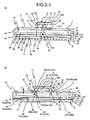
- the waveguide interface unit 42 includes: a first waveguide plate 51 having a thickness of about 2 to 5 millimeters (a thickness on which a screw hole can be formed) formed with screw holes 74 and 75 to fix the resin substrate 4; and a second waveguide plate 52 of a thin plate having a thickness of 0.5 to 1 millimeter (a thickness on which a waveguide and a slot hole can be formed) in contact with the first waveguide plate 51.
- the first waveguide plate 51 is provided with a rectangular opening in the direction of the plate thickness, and plural waveguides 61 are configured.
- the second waveguide plate 52 is provided with an opening to form plural waveguide trenches 62.
- the waveguide 61 is communicated to the waveguide trench 62 to constitute the waveguide 41.
- the waveguide 61 is directly connected to the waveguide 39.
- the first waveguide plate 51 and the second waveguide plate 52 are laminated and connected by positioning so that two reference holes 70 provided on each plate are superimposed at the same position of each place.
- the first and second waveguide plates 51 and 52 can be configured by laminating plural thin plates, respectively, and are not limited to one plate, respectively.
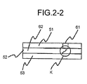
- a stepped surface can be formed at a corner of the waveguide by laminating plural plates having different sizes of holes at slight steps at the corner of a connection part between the waveguide 61 and the waveguide trench 62.
- Fig. 2-2 is a cross-sectional view of an example that a stepped surface is provided at the corner of the waveguide. As shown in Fig.
- a length of the hole forming the waveguide is sequentially changed in plural plates, and these plates are laminated to constitute the second waveguide plate 52, thereby forming a stepped surface having the length of the hole sequentially changed in the waveguide corner.
- propagation loss of the waveguide can be decreased by decreasing reflection at the waveguide corner.
- an iris can be provided near the corner to align. In this case, it is not necessary to laminate plural plates to provide a stepped surface. Therefore, the second waveguide plate 52 can be made much thinner. Productivity can be improved while maintaining the reduction effect of transmission loss.
- the power supply plate 53 is provided with power supply openings 63 (63a, 63b) having plural rectangular openings.
- the power-supply waveguide plate 54 is formed with plural power-supply waveguide trenches 64 (64a, 64b).
- the power-supply slot plate 55 is provided with power supply slots (holes) 65 (65a, 65b) having plural rectangular openings.
- the radiation waveguide plate 56 is formed with radiation waveguide trenches 66 (66a, 66b).
- the slot plate 57 is laid out with plural radiation slots 10 and radiation slots 11 having plural rectangular openings.
- the power supply openings 63, the power-supply waveguide trenches 64, the power supply slots 65, and the radiation waveguide trenches 66 are continuous with each other to constitute a power supply waveguide, and are connected to the waveguide 41.
- the radiation waveguide trench 66 (66a) is connected to the radiation slot 10.
- the radiation waveguide trench 66 (66b) is connected to the radiation slot 11.
- plural plates having slightly different sizes of holes can be laminated in a similar manner to that shown in Fig. 2-2 , thereby constituting a stepped surface at the corner of the waveguide.
- Plural (two or more) radiation slots 11 are laid out in series in the tube axis direction C to constitute slot rows in a state that opening directions (longitudinal directions) of the radiation slots are inclined at a suitable angle.
- Plural (two or more) slot rows are laid out to constitute a plane array.
- the radiation slot 11 receives the wave returning by reflection from a reflection unit after being transmitted from the radiation slot 10. Therefore, the radiation slot 11 functions as a reception radiation slot.
- a pair of (two) slot rows correspond to one reception channel. Because there are six slot rows, these constitute three receptions channels.
- One set of slot rows can be configured by constituting one subarray with plural radiation slots laid out in series, and arraying these subarrays in series.
- Each radiation slot 10 within the same slot row is electrically connected to one radiation waveguide trench 66a.
- the radiation waveguide trench 66a is formed with a trench to pierce through the radiation waveguide plate 56.
- the axial direction of the radiation waveguide trench 66a (longitudinal direction of the axis) coincides with the tube axis direction C in Fig. 3(b) , and each radiation slot 10 within the same slot row and the radiation waveguide trench 66a are laid out to face each other.
- Plural radiation waveguide trenches 66a are laid out in the orthogonal direction of the tube axis direction C, and each slot row of the radiation slot 10 is electrically connected to the radiation waveguide trench 66a laid out to face each other.
- Each radiation slot 11 within the same slot row is electrically connected to one radiation waveguide trench 66b.
- the radiation waveguide trench 66b is formed with a trench to pierce through the radiation waveguide plate 56.
- the axial direction of the radiation waveguide trench 66b (longitudinal direction of the axis) coincides with the tube axis direction C in Fig. 3(b) , and each radiation slot 11 within the same slot row and the radiation waveguide trench 66b are laid out to face each other.
- Plural radiation waveguide trenches 66b are laid out in the orthogonal direction of the tube axis direction C, and each slot row of the radiation slot 11 is electrically connected to the radiation waveguide trench 66b laid out to face each other.
- the power supply slot 65a is connected to the power-supply waveguide trench 64a.
- the power-supply waveguide trench 64a is formed with a trench to pierce through the power-supply waveguide plate 54.
- the power-supply waveguide trench 64a has a pair of branch trenches 641 branched to two directions in a T shape, and each of the pair of power supply slots 65a is connected to each of the pair of branch trenches 641.
- a longitudinal direction of the branch trenches 641 is orthogonally connected to the radiation waveguide trench 66a.
- a trench 642 is connected to branch to the branch trenches 641 from a branch part 643. That is, a transmission wave propagating the trench 642 is distributed by the branch trenches 641.
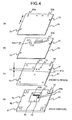
- the power supply slots 63a are connected to one end of a waveguide trench 62a.
- the power supply slots 63b are connected to one end of a waveguide trench 62b.
- the waveguide trenches 62a and 62b are formed with trenches to pierce through the waveguide plate 52.
- Plural power supply slots 63b are available, and each power supply slot 63b is connected to each waveguide trench 62b.
- one waveguide trench 62a and three waveguide trenches 62b are provided, and the trenches are formed in a smooth curved shape.
- Fig. 4(c) depicts the front surface of the first waveguide plate 51 in contact with the second waveguide plate 52
- Fig. 4(d) depicts the rear surface of the first waveguide plate 51 in contact with the resin substrate.
- the other end of the waveguide trench 62a is connected to the waveguide 61a having a rectangular opening.
- the other end of the waveguide trench 62b is connected to the waveguide 61b having a rectangular opening.
- the rear surface of the first waveguide plate 51 is provided with a choke trench 73 and screw holes (male screws) 74 and 75 laid out around each of the waveguides 61a and 61b.
- L2 denotes an interval between the waveguides 61a and 61b.
- screw holes 74 are laid out around each of the waveguides 61a and 61b.
- Four screw holes 75 in total are laid out at each of four corners of the first waveguide plate 51.
- a contact surface 80 provided around each of the waveguides 61a and 61b is milled (surface ground) to have high surface coarseness precision. Because the screw holes 74 are provided around each of the waveguides 61a and 61b, the contact surface of the waveguide 39 of the resin substrate 4 and that of the waveguide 61 of the antenna 5 are contacted more closely. It is needless to mention that the number and the layout of the screw holes are not limited to the example.
- a fitting surface 81 is provided around each screw hole 75.
- the contact surface 80 and the fitting surface 81 have the same heights.
- the other surface 82 of the rear surface of the first waveguide plate 51 has a plane surface slightly lower than the contact surface 80 and the fitting surface 81.
- a high-frequency signal input to and output from the waveguide 61 of the antenna 5 is connected to the radiation slots 10 and 11 via the waveguide 41 and the power supply waveguide configured inside the antenna 5.
- the radiation slot 10 transmits a wave
- the radiation slot 11 receives the wave.
- the first waveguide plate 51, the second waveguide plate 52, the power supply plate 53, the power-supply waveguide plate 54, the power-supply slot plate 55, the radiation waveguide plate 56, and the slot plate 57 use a thin stainless steel plates as their materials.
- the first waveguide plate 51, the second waveguide plate 52, the power supply plate 53, the power-supply waveguide plate 54, the power-supply slot plate 55, the radiation waveguide plate 56, and the slot plate 57 are prepared by having a thin plate processed in a desired shape to form a waveguide, a waveguide trench, and an opening (the waveguide 61, the waveguide trench 62, the waveguide opening 63, the power-supply waveguide trench 64, the power supply slot 65, the radiation waveguide trench 66, the radiation slots 10 and 11, the contact surface 82, the fitting surface 81, the choke trench 73, and the screw holes 74 and 75), and they are sequentially laminated from the bottom above.
- each plate In laminating, positioning pins are inserted into the two reference holes 70 provided on each plate. With this arrangement, the waveguide, the waveguide trench, and the opening of each plate can be accurately positioned.
- a desired processing shape of each plate can be processed by forming the same shape in the plate thickness direction. Therefore, each plate is processed in a desired shape, by punching of pressing a mold vertically to the plate surface, water-jet process of injecting pressured water flow vertically to the plate surface, and wire-cut discharge process. Therefore, each plate can be processed at low cost by a large amount. It is needless to mention that the processing methods are not limited to the above.
- connection surfaces of the plates are pressed equally by mounting weight from above the plates and by applying pressures with the pressing tool and the pressing machine.
- the laminated antenna is put into the heating furnace, thereby heating the whole antenna at a predetermined temperature at which the connection surfaces can be diffusion bonded in the solid phase.
- the connection surfaces of the contacted plates are connected, thereby integrally connecting the antenna 5.
- the first waveguide plate 51, the second waveguide plate 52, the power supply plate 53, the power-supply waveguide plate 54, the power-supply slot plate 55, the radiation waveguide plate 56, and the slot plate 57 are fixed and integrated. Because the connection surfaces of the plates are substantially equally connected by the diffusion bonding, a gap between the connected plates can be eliminated. Therefore, interference between adjacent waveguides can be suppressed, and isolation characteristic between transmission channels or between reception channels can be improved.
- the waveguide interface unit 42 constituting the antenna 5 and the antenna unit 43 are integrally connected is explained above.
- the waveguide interface unit 42 and the antenna unit 43 can be separately diffusion bonded, and thereafter both can be fixed together by fastening by connection or with screws.
- a gap is formed between the connection surfaces of the waveguide interface unit 42 and the antenna unit 43. Therefore, a choke trench is required to be additionally provided between near different waveguides so that the waveguides do not interfere with each other.
- the connection surfaces need to be processed in high precision.
- integrating the waveguide interface unit 42 with the antenna unit 43 using the diffusion bonding can provide a simpler configuration than that when the waveguide interface unit 42 and the antenna unit 43 are connected as separate units, and can decrease production cost and improve isolation characteristic of waveguides.
- Fig. 5-1(a) is an upper surface perspective view (a state that the lid unit 22 is removed) of a front surface of the high-frequency package 2
- Fig. 5-1(b) is a lower surface perspective view of a rear surface of the high-frequency package
- Fig. 5-2(c) is a part perspective view of a structure of a microstrip-line waveguide converter of the high-frequency package 2
- Fig. 5-2(d) is a part cross-sectional view of an inner structure of the high-frequency package 2.
- Fig. 6 is a perspective view of a rear surface side (a connection side with the antenna 5) of a configuration of the resin substrate 4.
- the semiconductor chip 21 is accommodated within the cavity 110 provided on the dielectric multilayer substrate 20.
- the dielectric multilayer substrate 20 is configured by laminating at least a dielectric multilayer substrate 201, a dielectric multilayer substrate 202, and a dielectric multilayer substrate 203.
- the seal ring 500 having an 8-shape (a shape that an outer frame is connected to the surrounding of an inner frame) having the lid unit (22) not shown connected on the upper surface by seam welding or the like is connected to the front surface of the upper layer of the dielectric multilayer substrate 20 by silver waxing or soldering. As shown in Fig.
- the resin substrate 4 is formed with plural waveguides 39 (39a, 39b) and screw holes 79.
- the front layer of the resin substrate 4 is provided with a ground conductor layer 140 formed to surround the waveguide 39, and the waveguide 39 is grounded to the ground conductor layer 140.
- the ground conductor layer 140 at the rear surface side of the resin substrate 4 is closely adhered to the fitting surface 81 of the antenna 5.
- the front layer (upper surface) of the dielectric multilayer substrate 203 is laid out with the above-described microstrip line 27 and a ground conductor 102.
- the microstrip line 27 can constitute a coplanar line by having a ground conductor laid out around, or can constitute a grounded coplanar line by having a ground conductor laid out with plural ground conductor vias and connected.
- One end of the microstrip line 27 is connected to a conductor terminal (pad) 211 provided on the semiconductor chip 21 via the conductive wire 111.
- the other end of the microstrip line 27 is integrally connected to the ground conductor 102.
- a ground conductor 103 is provided on the lower surface of the dielectric multilayer substrate 203.
- the ground conductor 103 is provided with a rectangular opening 105.
- the ground conductor 102 is connected to the ground conductor 103 via plural ground conductor vias 28a at predetermined intervals (intervals equal to or smaller than a signal propagation wavelength ⁇ /4 within the dielectric multilayer substrate).
- the ground conductor vias 28a are laid out in a U shape along the surrounding of three sides excluding one side at the microstrip line 27 side to surround the opening 105.
- a ground conductor 104 is provided on the lower surface of the dielectric multilayer substrate 202.
- a rectangular opening 106 is formed on the ground conductor 104.
- the ground conductor 103 is connected to the ground conductor 104 via plural ground conductor vias 28b at predetermined intervals (intervals equal to or smaller than a signal propagation wavelength ⁇ /4 within the dielectric multilayer substrate).
- the ground conductor vias 28b are laid out in a rectangular ring shape along the surrounding of the opening 106 to encircle the opening 106.
- the opening 106 is larger than the opening 105, and the ground conductor via 28a and the ground conductor via 28b are connected at a stage by sandwiching the ground conductor 103.
- a ground conductor 142 is provided on the lower surface of the dielectric multilayer substrate 201.
- a rectangular opening 107 is formed on the ground conductor 142.
- the ground conductor 104 is connected to the ground conductor 142 via plural ground conductor vias 28c at predetermined intervals (intervals equal to or smaller than a signal propagation wavelength ⁇ /4 within the dielectric multilayer substrate).
- the ground conductor vias 28c are laid out in a rectangular ring shape along the surrounding of the opening 107 to encircle the opening 107.
- the opening 107 is larger than the opening 106, and the ground conductor via 28b and the ground conductor via 28c are connected at a stage by sandwiching the ground conductor 104.
- the opening 107 of the dielectric multilayer substrate 201 constitutes waveguide terminals 33.
- the waveguide terminals 33 are configured in the opening provided in the ground conductor 142 on the rear surface of the high-frequency package 2.
- Three reception waveguide terminals 33c and one transmission waveguide terminal 33a are provided as the waveguide terminals 33.
- each waveguide terminal 33 can be laid out at a quite different position from the positions and the intervals of the power supply slots 65 inside the antenna 5.
- the interval between the waveguide terminal 33a ad the waveguide terminal 33b can be set approximately the same as an interval L2 between the waveguide 61a and the waveguide 61b.
- the number and the laid out of the waveguide terminals 33 are not limited to this example.
- the dielectric part encircled by the ground conductor via 28a, the ground conductor via 28b, and the ground conductor via 28c, and the openings 105, 106, and 107 constitute the dielectric waveguide 32.
- An impedance conversion is performed between the dielectric waveguide 32 and the microstrip line 27.
- the microstrip-line waveguide converter performs a conversion operation between the microstrip mode and the waveguide mode.
- a milliwave-band high-frequency signal (transmission signal) output from the semiconductor chip 21 (21a) is transmitted to the dielectric waveguide 30 through the microstrip line 27, and is output from the waveguide terminal 33(33a).
- the high-frequency signal output from the waveguide terminal 33(33a) is input to the waveguide 61 of the antenna 5 through the waveguide 39 of the resin substrate 4.
- the high-frequency signal input to the waveguide 61 of the antenna 5 is electrically connected to the radiation slot 10 of the antenna 5 via each waveguide (the waveguide 61a, the waveguide trench 62a, the power-supply waveguide trench 64a, and the radiation waveguide trench 66a) inside the antenna 5 and the power supply slots (the power supply slot 63a, the power supply slot 65a), so that a transmission wave is radiated (output) from the radiation slot 10.
- the transmission wave output from the radiation slot 10 is reflected from a reflector reflecting the outer wave, and is reflected to the antenna 5.
- the radiation slot 11 receives the reception wave returned to the antenna 5.
- the reception signal received by this radiation slot 11 is connected to the power supply slot 65b via the waveguide trench 66b of the antenna 5.
- the reception signal connected to the power supply slot 65b is input to the waveguide 61 via each waveguide (the power-supply waveguide trench 64b, the waveguide trench 62b, and the waveguide 61b) inside the antenna 5 and the power supply slot 63b.
- the reception signal input to the waveguide 61 is input to the waveguide terminal 33 through the waveguide 39 of the resin substrate 4.
- the reception signal (high-frequency signal) input to the waveguide terminal 33 is transmitted to the strip line 27 by the dielectric waveguide 30, and is input to the semiconductor chip 21 (21b).
- the transmission semiconductor chip 21a that outputs a transmission signal and the reception semiconductor chip 21b that receives an input reception signal are accommodated in different cavity spaces 800a and 800b, respectively.
- An intermediate frame of the seal ring 500 is set between the cavity spaces 800a and 800b so that there is not wave interference therebetween. Therefore, isolation is secured between the semiconductor chips 21a and 21b.
- the waveguide terminals 33 are connected to the waveguide 39 of the resin substrate 4 via the plural conductive connection members 32 laid out in a ring shape as described above.
- the resin substrate 4 is brought into contact with the antenna 5, and the waveguide 39 is connected to the waveguide 61 as described above.
- the waveguide 39 of the resin substrate 4 is provided with the ground conductor layer 140 on the inner periphery of the opening of the waveguide 39 as described above.
- the ground conductive layer 140 is connected to a ground conductive layer 141 provided on the upper and lower surfaces of the resin substrate 140 on the periphery of the opening of the waveguide 39.
- the ground conductive layer 141 is connected to the ground conductive layer 142 on the lower surface of the dielectric multilayer substrate 201 via the conductive connection members 32 as described above.
- the resin substrate 4 and the antenna 5 are fastened and are brought into close contact with each other by crews as described above.
- a gap is generated between the resin substrate 4 and the antenna 5 on the connection surface of the resins substrate 4 and the antenna 5 excluding the periphery of the fastened part.
- the gap is large, a signal leakage occurs at the connection part between the waveguide 39 and the waveguide 61.
- the choke trench 73 is provided on the upper surface (rear surface) of the antenna 5, a short surface is electrically formed, and the signal leakage between the waveguide 39 and the waveguide 61 is suppressed.
- the choke trench 73 is separated from the waveguide 61 with a signal propagation wavelength ⁇ /4 within the free space, and has a depth of a signal propagation wavelength ⁇ /4 within the free space.
- the high-frequency package 20 has a signal transmission path for transmitting and receiving an electric signal to and from the resin substrate 4.
- the signal transmission path is connected to a waveguide via 24a and the conductor strip line (signal line) 25 of the substrate inner layer, in the inner layer of the dielectric multilayer substrate of the high-frequency package 20.
- the conductor via 24a is connected to a conductor via 24b in the inner layer of the substrate via the conductor strip line 25 in the inner layer of the substrate.
- Each conductor via 24b is connected to a conductor terminal 171 provided on the outer periphery of the lower surface of the high-frequency package 20.
- the conductor terminals 171 are connected in parallel to plural (two rows in the example shown in Fig. 5-1(b) ) conductive connection members 31 laid out on the outer periphery of the high-frequency package 20. That is, two conductive connection members 31 connected to one conductor terminal 171 are connected in parallel and pass the same signal.
- the conductive connection members 31 are connected to a conductor terminal 172 provided on the front surface of the resin substrate 4. Accordingly plural rows of the conductive connection members 31 connected to the outer periphery of the high-frequency package 20 are connected to each other in parallel. Therefore, even when the conductive connection members 31 provided at the outermost side of the high-frequency package 20 are disconnected, a disconnection of a signal between the resin substrate 4 and the high-frequency package 20 can be prevented when the conductive connection members 31 connected in parallel to the inside of the high-frequency package 20 are not disconnected.
- the conductor terminal 172 is connected to a conductor via 151 in the inner layer of the resin substrate and is connected to a conductor line 150 in the inner layer of the substrate.
- the conductor line 150 is connected to a conductor terminal 173 of the front layer of the resin substrate 4 via a conductor via 160 in the inner layer of the substrate.
- the conductor terminal 173 is connected to a conductor terminal of the electronic part 3 via a conductive member (lead) 122. That is, the resin substrate 4 and the high-frequency package 20 are electrically connected to each other via plural conductive connection members 31 connected to the outermost side of the high-frequency package 20.
- the semiconductor chip 21 within the high-frequency package 2 and the electronic part 3 on the resin substrate 4 can transmit low-frequency electric signals such as a control signal, a monitor signal, a video signal, and a power supply bias, with each other.
- the present embodiment includes: a slot plate having plural radiation slots laid out in inclination; a radiation waveguide plate formed with plural rows of waveguide trenches having radiation slots laid out in respective pipe axis directions; a power-supply slot plate formed with plural power supply slots brought into contact with the radiation waveguide plate and connected to respective waveguide trenches; a power-supply waveguide plate formed with plural waveguides brought into contact with the power-supply slot plate and connected to respective power supply slots; and a power supply plate formed with plural waveguide openings brought into contact with the power-supply waveguide plate and connected to respective waveguides.
- the plates are diffusion bonded to configure an integrally connected antenna (slot antenna).
- the embodiment further includes: a resin substrate fixed to the front surface of the power supply plate of the antenna, having plural waveguide openings communicated to respective waveguide openings of the antenna, and mounted with conductor terminals, ground conductors, and electronic parts; and a high-frequency package having a dielectric substrate mounted with a high-frequency semiconductor element, and a lid unit accommodating the dielectric substrate and the high-frequency semiconductor element, and connected to a resin substrate via plural conductive connection members.
- the high-frequency package has a waveguide terminal formed with a dielectric opening in a ground conductor, a conductor terminal, and a ground conductor, at the outside of the package, having the waveguide terminal and a high-frequency signal terminal of a high-frequency semiconductor element connected to each other via a dielectric waveguide, and having a waveguide terminal of the high-frequency package and a waveguide opening of the resin substrate laid out to face each other.
- Plural conductive connection members are laid out to surround the waveguide terminal of the high-frequency package and the waveguide opening of the resin substrate. The conductor terminal of the high-frequency package, the ground conductor, the conductor terminal of the resin substrate, and the ground conductor are connected.
- the antenna 5 constituting a slot antenna is integrally configured.
- plural waveguides 41 and power supply waveguides connected to the radiation slot and having a complex shape can be configured within the antenna 5 at low cost.
- an interval between adjacent waveguides can be taken longer at the radiation slot side than an interval between adjacent waveguide terminals 33, and the waveguides can be laid out in a desired shape and at free positions.
- the interval L2 in Fig. 4 can be made smaller than the interval L1 in Fig. 1 .
- the high-frequency module 1 can be produced at low cost.
- the resin substrate organic substrate having a high-frequency package waxed (BGA connection) and the antenna can be directly connected to each other via both waveguide terminal.
- the connection structure can be made thinner.
- a waveguide plate waveguide adapter
- a waveguide interface needs to be taken between the antenna and the resin substrate by fixing the antenna, the waveguide plate, and the resin substrate with screws.
- a plate material A having a waveguide trench configured by milling and a plate material B having a waveguide opening need to be superimposed with each other to configure a waveguide adapter.
- the trench of the plate material A is formed by milling, and a cavity is provided in the waveguide corner to align the waveguide corner (for example, see Japanese Patent Application Laid-open No. 2004-172688 ). Therefore, it has been difficult to decrease the thickness of the waveguide adapter.
- a waveguide adapter is not necessary. Because a stepped surface can be configured in the waveguide corner by forming holes in thin plates and by integrally connecting the plural thin plates by diffusion bonding, no cavity is left in the waveguide corner, and the thickness required for the layout of the waveguide can be decreased.
- a waveguide can be configured having a size that a height ratio of an E surface to an H surface of a waveguide cross section is smaller than a normal 1:2 (for example, a height ratio of the E surface to the H surface is equal to 1:2 to 1:1.16), without a constraint of a waveguide trench depth based on the milling. Therefore, the antenna can be made thinner than that when a waveguide adapter is used.
- a thin antenna having a waveguide interface can be configured to have a thickness half of that when the waveguide adapter is used.
- a waveguide terminal of the high-frequency package 2 can be easily connected to a waveguide of the resin substrate 4 by connecting the resin substrate 4 to the high-frequency package 2 using plural conductive connection members 31 and 32 (ball grid array). Further, a conductor terminal of the high-frequency package 2 can be easily connected to a conductor terminal of the resin substrate 4. Accordingly, low-frequency electric signals such as a control signal, a monitor signal, a video signal, and a power supply bias can be transmitted between the high-frequency package 2 and the resin substrate 4 while simultaneously transmitting a high-frequency signal from the high-frequency package 2 to the waveguide 39 of the resin substrate 4.
- the waveguide of the resin substrate 4 and the waveguide terminal of the high-frequency package 2 are integrally connected with plural conductive connection members 32, and because the antenna 5 integrally constitutes the waveguide, the waveguides are isolated on only the connection surface of the waveguide of the resin substrate 4 and the waveguide of the antenna 5, between the waveguide terminal of the high-frequency package 2 and the radiation slot. Therefore, a place having a possibility of a signal leakage in the connection part of the waveguide becomes only the connection surface between the waveguide of the resin substrate 4 and the waveguide of the antenna 5. Therefore, it is sufficient that a choke trench is provided around the waveguide on only the connection surface. Accordingly, the choke trench becomes minimum necessary, and the processing cost can be suppressed and a leakage signal can be decreased.
- the waveguide 41 is constituted in the inside of the antenna 5, so that air of a specific inductive capacity of one (1) flows. Therefore, the dielectric loss becomes remarkably small. Accordingly, a high-frequency signal of a milliwave band input to and output from the waveguide terminal 33 of the high-frequency package 2 can be input and output between the radiation slots 10 and 11 with remarkably high efficiency via the waveguide 41 and with low loss.
- the high-frequency module having the antenna according to the present embodiment can be suitably applied to a milliwave-radio communication device and a milliwave radar that input and output milliwave-band high-frequency signals.
Landscapes
- Engineering & Computer Science (AREA)
- Manufacturing & Machinery (AREA)
- Waveguide Aerials (AREA)
- Variable-Direction Aerials And Aerial Arrays (AREA)
Applications Claiming Priority (2)
| Application Number | Priority Date | Filing Date | Title |
|---|---|---|---|
| JP2006028084 | 2006-02-06 | ||
| PCT/JP2007/051660 WO2007091470A1 (fr) | 2006-02-06 | 2007-02-01 | Module à haute fréquence |
Publications (3)
| Publication Number | Publication Date |
|---|---|
| EP1983614A1 true EP1983614A1 (fr) | 2008-10-22 |
| EP1983614A4 EP1983614A4 (fr) | 2010-01-06 |
| EP1983614B1 EP1983614B1 (fr) | 2016-08-31 |
Family
ID=38345073
Family Applications (1)
| Application Number | Title | Priority Date | Filing Date |
|---|---|---|---|
| EP07707846.7A Ceased EP1983614B1 (fr) | 2006-02-06 | 2007-02-01 | Module à haute fréquence |
Country Status (5)
| Country | Link |
|---|---|
| US (1) | US8040286B2 (fr) |
| EP (1) | EP1983614B1 (fr) |
| JP (1) | JP4394147B2 (fr) |
| CN (1) | CN101395759B (fr) |
| WO (1) | WO2007091470A1 (fr) |
Cited By (6)
| Publication number | Priority date | Publication date | Assignee | Title |
|---|---|---|---|---|
| EP2267832A1 (fr) * | 2009-06-11 | 2010-12-29 | Imec | Système intégré comprenant un guide d'ondes sur un appareil de couplage de microruban |
| CN102064380A (zh) * | 2010-10-26 | 2011-05-18 | 李峰 | 波导平板阵列天线 |
| EP3252499A1 (fr) * | 2016-05-31 | 2017-12-06 | Honeywell International Inc. | Antenne réseau à commande de phase active numérique intégrée et système d'évitement de collision de bout d'aile |
| US10389006B2 (en) | 2014-07-30 | 2019-08-20 | Fujitsu Limited | Electronic apparatus and manufacturing method thereof |
| WO2019166064A1 (fr) * | 2018-03-01 | 2019-09-06 | Conti Temic Microelectronic Gmbh | Système radar servant à détecter l'environnement d'un véhicule automobile avec une antenne en matière plastique |
| EP3647807B1 (fr) * | 2018-10-29 | 2023-12-13 | Aptiv Technologies Limited | Ensemble radar doté d'une transition à fente par l'intermédiaire d'une carte de circuit imprimé |
Families Citing this family (52)
| Publication number | Priority date | Publication date | Assignee | Title |
|---|---|---|---|---|
| EP1854637B1 (fr) * | 2005-03-03 | 2011-03-02 | Toshiba TEC Kabushiki Kaisha | Imprimante et dispositif de communication a puce a circuit integre |
| JP4990353B2 (ja) * | 2007-03-14 | 2012-08-01 | 三菱電機株式会社 | 高周波パッケージ |
| EP2261514A4 (fr) * | 2008-03-25 | 2013-06-26 | Mitsubishi Electric Corp | Ensemble conduit empilé et procédé de fixation de vis pour pièce de conduit |
| US8564478B2 (en) * | 2008-03-31 | 2013-10-22 | Kyocera Corporation | High-frequency module and method of manufacturing the same, and transmitter, receiver, transceiver, and radar apparatus comprising the high-frequency module |
| JP5216848B2 (ja) * | 2008-03-31 | 2013-06-19 | 京セラ株式会社 | 高周波モジュールおよびその製造方法ならびに該高周波モジュールを備えた送信器、受信器、送受信器およびレーダ装置 |
| JP4592786B2 (ja) * | 2008-06-18 | 2010-12-08 | 三菱電機株式会社 | アンテナ装置及びレーダ |
| JP4996640B2 (ja) * | 2009-03-10 | 2012-08-08 | 株式会社東芝 | アンテナ装置、レーダ装置 |
| US8760342B2 (en) * | 2009-03-31 | 2014-06-24 | Kyocera Corporation | Circuit board, high frequency module, and radar apparatus |
| KR101327375B1 (ko) * | 2009-03-31 | 2013-11-08 | 쿄세라 코포레이션 | 도파 구조체, 도파 구조체를 포함하는 고주파 모듈, 및 레이더 장치 |
| US8508029B2 (en) * | 2011-09-29 | 2013-08-13 | Broadcom Corporation | Semiconductor package including an integrated waveguide |
| US9570420B2 (en) | 2011-09-29 | 2017-02-14 | Broadcom Corporation | Wireless communicating among vertically arranged integrated circuits (ICs) in a semiconductor package |
| US9160049B2 (en) | 2011-11-16 | 2015-10-13 | Commscope Technologies Llc | Antenna adapter |
| US8558746B2 (en) | 2011-11-16 | 2013-10-15 | Andrew Llc | Flat panel array antenna |
| US8866687B2 (en) | 2011-11-16 | 2014-10-21 | Andrew Llc | Modular feed network |
| DE102012203293B4 (de) | 2012-03-02 | 2021-12-02 | Robert Bosch Gmbh | Halbleitermodul mit integriertem Wellenleiter für Radarsignale |
| JP6102106B2 (ja) * | 2012-07-20 | 2017-03-29 | 株式会社デンソー | レーダ装置 |
| KR101659827B1 (ko) * | 2012-12-20 | 2016-09-26 | 가부시키가이샤 무라타 세이사쿠쇼 | 멀티밴드용 안테나 |
| CN103151340B (zh) * | 2013-02-08 | 2016-04-20 | 日月光半导体制造股份有限公司 | 天线封装模块及其制造方法 |
| US9130254B1 (en) | 2013-03-27 | 2015-09-08 | Google Inc. | Printed waveguide transmission line having layers bonded by conducting and non-conducting adhesives |
| US9123979B1 (en) | 2013-03-28 | 2015-09-01 | Google Inc. | Printed waveguide transmission line having layers with through-holes having alternating greater/lesser widths in adjacent layers |
| US9142872B1 (en) | 2013-04-01 | 2015-09-22 | Google Inc. | Realization of three-dimensional components for signal interconnections of electromagnetic waves |
| US9806431B1 (en) * | 2013-04-02 | 2017-10-31 | Waymo Llc | Slotted waveguide array antenna using printed waveguide transmission lines |
| DE102014200660A1 (de) * | 2014-01-16 | 2015-07-16 | Conti Temic Microelectronic Gmbh | Sende- und Empfangseinheit für Radarsignale und Verfahren zur Herstellung derselben |
| EP3118927B9 (fr) * | 2014-03-11 | 2021-08-04 | Mitsubishi Electric Corporation | Boîtier haute fréquence |
| WO2015172291A1 (fr) * | 2014-05-12 | 2015-11-19 | 华为技术有限公司 | Antenne et dispositif sans fil |
| WO2017078184A1 (fr) * | 2015-11-05 | 2017-05-11 | Nidec Elesys Corporation | Antenne à fentes |
| US11038263B2 (en) * | 2015-11-12 | 2021-06-15 | Duke University | Printed cavities for computational microwave imaging and methods of use |
| JP2019047141A (ja) * | 2016-03-29 | 2019-03-22 | 日本電産エレシス株式会社 | マイクロ波ic導波路装置モジュール、レーダ装置およびレーダシステム |
| US10490905B2 (en) | 2016-07-11 | 2019-11-26 | Waymo Llc | Radar antenna array with parasitic elements excited by surface waves |
| JP6368342B2 (ja) * | 2016-09-09 | 2018-08-01 | 株式会社フジクラ | アンテナ装置及びその製造方法 |
| DE112016007546T5 (de) | 2016-12-26 | 2019-09-19 | Mitsubishi Electric Corporation | Radarvorrichtung |
| CN107181043B (zh) * | 2017-05-22 | 2020-03-27 | 上海安费诺永亿通讯电子有限公司 | 一种无线移动终端 |
| US10199336B2 (en) * | 2017-05-24 | 2019-02-05 | Advanced Semiconductor Engineering, Inc. | Antenna package device |
| US11500059B2 (en) * | 2017-07-11 | 2022-11-15 | Mitsubishi Electric Corporation | Radar device |
| US11881626B2 (en) * | 2018-05-01 | 2024-01-23 | Robin Radar Facilities Bv | Radar system comprising two back-to-back positioned radar antenna modules, and a radar system holding an antenna module with cavity slotted-waveguide antenna arrays for radiating and receiving radar wave signals |
| KR102089285B1 (ko) | 2018-07-17 | 2020-03-16 | 삼성전자주식회사 | 안테나 모듈 |
| US10700440B1 (en) | 2019-01-25 | 2020-06-30 | Corning Incorporated | Antenna stack |
| US10749256B1 (en) * | 2019-01-30 | 2020-08-18 | Raytheon Company | Waveguide adapter for slot antennas |
| CN113330324B (zh) | 2019-01-31 | 2023-06-06 | 三菱电机株式会社 | 雷达装置和信号处理方法 |
| US11128023B2 (en) * | 2019-02-22 | 2021-09-21 | Texas Instruments Incorporated | Substrate design for efficient coupling between a package and a dielectric waveguide |
| EP3935688A1 (fr) * | 2019-03-07 | 2022-01-12 | Huawei Technologies Co., Ltd. | Dispositif d'antenne et son procédé de fabrication |
| KR102290019B1 (ko) | 2019-05-29 | 2021-08-17 | 주식회사 아모텍 | 레이더 안테나 |
| JP7493922B2 (ja) | 2019-08-26 | 2024-06-03 | キヤノン株式会社 | 発振器、撮像装置 |
| US11522268B2 (en) * | 2020-01-09 | 2022-12-06 | Texas Instruments Incorporated | Wireless device with substrate to antenna coupling |
| US11378683B2 (en) * | 2020-02-12 | 2022-07-05 | Veoneer Us, Inc. | Vehicle radar sensor assemblies |
| DE102020211254A1 (de) * | 2020-09-08 | 2022-03-10 | Conti Temic Microelectronic Gmbh | Radarsystem zur Umgebungserfassung mit einer Wellenleiterantenne gebildet aus einer Platine und einem Formteil |
| US12401128B2 (en) | 2021-03-05 | 2025-08-26 | Huber+Suhner Ag | Waveguide antenna |
| JP7793648B2 (ja) * | 2021-05-10 | 2026-01-05 | サーブ リミティド-アブダビ | 広帯域二重偏波平面アンテナアレイ |
| US12355151B2 (en) * | 2021-05-17 | 2025-07-08 | HJWAVE Co., Ltd. | Antenna structure with reduced angle error |
| DE102021214637A1 (de) * | 2021-12-17 | 2023-06-22 | Robert Bosch Gesellschaft mit beschränkter Haftung | Hochfrequenzbaugruppe für Radarsensoren |
| CN117423964A (zh) * | 2022-07-19 | 2024-01-19 | 群创光电股份有限公司 | 电子装置以及电子装置的制造方法 |
| DE102024111788A1 (de) * | 2024-04-26 | 2025-10-30 | Golden Devices Gmbh | Hochfrequenzbauteil |
Family Cites Families (32)
| Publication number | Priority date | Publication date | Assignee | Title |
|---|---|---|---|---|
| JPH0789603B2 (ja) | 1986-03-12 | 1995-09-27 | 株式会社日立製作所 | 導波管形スロツトアレイアンテナ |
| JPH0366214U (fr) * | 1989-07-24 | 1991-06-27 | ||
| JPH0366214A (ja) | 1989-08-05 | 1991-03-20 | Mitsubishi Electric Corp | 高周波電力増幅回路 |
| EP0527178A4 (en) | 1990-04-30 | 1993-11-24 | Commonwealth Scientific & Industrial Research Organisation ( C.S.I.R.O. ) | A flat plate antenna |
| CA2066887C (fr) | 1991-05-06 | 1996-04-09 | Harry Wong | Repartiteur de puissance rf a cavite a plat |
| JPH053405A (ja) | 1991-06-25 | 1993-01-08 | Asahi Chem Ind Co Ltd | 導波管結合構造 |
| JPH056921A (ja) | 1991-06-28 | 1993-01-14 | Toshiba Corp | 半導体装置 |
| JPH056921U (ja) * | 1991-07-01 | 1993-01-29 | 旭化成工業株式会社 | 高剛性アンテナ |
| JPH07106843A (ja) | 1993-09-29 | 1995-04-21 | Japan Atom Energy Res Inst | 高周波出力アンテナ |
| JPH07106847A (ja) * | 1993-10-07 | 1995-04-21 | Nippon Steel Corp | 漏れ波導波管スロットアレーアンテナ |
| JPH10313214A (ja) | 1997-05-13 | 1998-11-24 | Nippon Steel Corp | アンテナおよびその製造方法 |
| US6028562A (en) * | 1997-07-31 | 2000-02-22 | Ems Technologies, Inc. | Dual polarized slotted array antenna |
| KR100463911B1 (ko) | 1997-10-01 | 2004-12-30 | 히다치 가세고교 가부시끼가이샤 | 광정보처리장치 |
| JPH11344537A (ja) | 1998-06-03 | 1999-12-14 | Matsushita Electric Ind Co Ltd | 半導体デバイス |
| JP3812203B2 (ja) | 1999-02-17 | 2006-08-23 | 三菱電機株式会社 | 導波管スロットアレイアンテナ |
| JP2000261239A (ja) | 1999-03-05 | 2000-09-22 | Fujitsu Ltd | 導波管スロットアンテナ |
| SE514557C2 (sv) | 1999-07-09 | 2001-03-12 | Ericsson Telefon Ab L M | Anordning för bruk i en gruppantenn för sändning och mottagning på minst en frekvens i minst två polarisationer |
| WO2001018901A1 (fr) * | 1999-09-02 | 2001-03-15 | Commonwealth Scientific And Industrial Research Organisation | Structure d'alimentation pour guides d'ondes electromagnetiques |
| SE517155C2 (sv) * | 1999-09-08 | 2002-04-23 | Ericsson Telefon Ab L M | Fördelningsnät, samt antennanordning innefattande sådant fördelningsnät |
| US6870438B1 (en) * | 1999-11-10 | 2005-03-22 | Kyocera Corporation | Multi-layered wiring board for slot coupling a transmission line to a waveguide |
| JP3631667B2 (ja) * | 2000-06-29 | 2005-03-23 | 京セラ株式会社 | 配線基板およびその導波管との接続構造 |
| JP2001144512A (ja) | 1999-11-10 | 2001-05-25 | Kyocera Corp | 配線基板およびその導波管との接続構造 |
| JP3428575B2 (ja) | 2000-09-07 | 2003-07-22 | 三菱電機株式会社 | 高周波モジュールおよび高周波無線装置 |
| JP4021150B2 (ja) * | 2001-01-29 | 2007-12-12 | 沖電気工業株式会社 | スロットアレーアンテナ |
| EP1753085A1 (fr) | 2001-03-21 | 2007-02-14 | Microface Co. Ltd | Antenne à fentes en guide d'ondes et procédé de fabrication |
| JP2003086728A (ja) | 2001-07-05 | 2003-03-20 | Matsushita Electric Ind Co Ltd | 高周波回路の製作方法及びそれを用いた装置 |
| JP2003318642A (ja) | 2002-04-25 | 2003-11-07 | Japan Radio Co Ltd | 導波管スロットアレーアンテナ |
| DE10222838A1 (de) | 2002-05-21 | 2003-12-04 | Marconi Comm Gmbh | Sektorantenne in Hohlleitertechnik |
| JP2004088504A (ja) | 2002-08-27 | 2004-03-18 | Kyocera Corp | 高周波素子収納用パッケージ |
| JP3846585B2 (ja) | 2002-11-18 | 2006-11-15 | 三菱電機株式会社 | 導波管ベンド、導波管プレートおよび高周波装置 |
| JP2005217865A (ja) | 2004-01-30 | 2005-08-11 | Toko Inc | 誘電体導波管スロットアンテナ |
| US8170643B2 (en) * | 2005-11-22 | 2012-05-01 | Bsd Medical Corporation | System and method for irradiating a target with electromagnetic radiation to produce a heated region |
-
2007
- 2007-02-01 US US12/158,088 patent/US8040286B2/en active Active
- 2007-02-01 WO PCT/JP2007/051660 patent/WO2007091470A1/fr not_active Ceased
- 2007-02-01 CN CN2007800018094A patent/CN101395759B/zh not_active Expired - Fee Related
- 2007-02-01 JP JP2007557803A patent/JP4394147B2/ja active Active
- 2007-02-01 EP EP07707846.7A patent/EP1983614B1/fr not_active Ceased
Cited By (11)
| Publication number | Priority date | Publication date | Assignee | Title |
|---|---|---|---|---|
| EP2267832A1 (fr) * | 2009-06-11 | 2010-12-29 | Imec | Système intégré comprenant un guide d'ondes sur un appareil de couplage de microruban |
| CN102064380A (zh) * | 2010-10-26 | 2011-05-18 | 李峰 | 波导平板阵列天线 |
| US10389006B2 (en) | 2014-07-30 | 2019-08-20 | Fujitsu Limited | Electronic apparatus and manufacturing method thereof |
| EP3252499A1 (fr) * | 2016-05-31 | 2017-12-06 | Honeywell International Inc. | Antenne réseau à commande de phase active numérique intégrée et système d'évitement de collision de bout d'aile |
| US10613216B2 (en) | 2016-05-31 | 2020-04-07 | Honeywell International Inc. | Integrated digital active phased array antenna and wingtip collision avoidance system |
| US11668817B2 (en) | 2016-05-31 | 2023-06-06 | Honeywell International Inc. | Integrated digital active phased array antenna and wingtip collision avoidance system |
| WO2019166064A1 (fr) * | 2018-03-01 | 2019-09-06 | Conti Temic Microelectronic Gmbh | Système radar servant à détecter l'environnement d'un véhicule automobile avec une antenne en matière plastique |
| CN111758044A (zh) * | 2018-03-01 | 2020-10-09 | 康蒂-特米克微电子有限公司 | 用于机动车辆周围环境检测的、带塑料天线的雷达系统 |
| US11604273B2 (en) | 2018-03-01 | 2023-03-14 | Conti Temic Microelectronic Gmbh | Radar system for detecting the environment of a motor vehicle having a plastic antenna |
| CN111758044B (zh) * | 2018-03-01 | 2024-11-08 | 大陆智行德国有限公司 | 用于机动车辆周围环境检测的、带塑料天线的雷达系统 |
| EP3647807B1 (fr) * | 2018-10-29 | 2023-12-13 | Aptiv Technologies Limited | Ensemble radar doté d'une transition à fente par l'intermédiaire d'une carte de circuit imprimé |
Also Published As
| Publication number | Publication date |
|---|---|
| JPWO2007091470A1 (ja) | 2009-07-02 |
| WO2007091470A1 (fr) | 2007-08-16 |
| US8040286B2 (en) | 2011-10-18 |
| CN101395759B (zh) | 2011-06-22 |
| JP4394147B2 (ja) | 2010-01-06 |
| CN101395759A (zh) | 2009-03-25 |
| US20090079648A1 (en) | 2009-03-26 |
| EP1983614B1 (fr) | 2016-08-31 |
| EP1983614A4 (fr) | 2010-01-06 |
Similar Documents
| Publication | Publication Date | Title |
|---|---|---|
| EP1983614B1 (fr) | Module à haute fréquence | |
| US9648725B2 (en) | High-frequency circuit package and sensor module | |
| US12080661B2 (en) | Integrated structures with antenna elements and IC chips employing edge contact connections | |
| US5488380A (en) | Packaging architecture for phased arrays | |
| US8592960B2 (en) | Leadframe package with integrated partial waveguide interface | |
| EP0491161A1 (fr) | Boîtier d'interconnexion pour des composants de circuit | |
| CN111525284A (zh) | 多频复合大功率瓦片式有源相控阵天线 | |
| US6081988A (en) | Fabrication of a circuit module with a coaxial transmission line | |
| CN116895614B (zh) | 一种三维异构集成的毫米波系统封装结构 | |
| US5945897A (en) | Compliant RF coaxial interconnect | |
| US6081989A (en) | Fabrication of circuit modules with a transmission line | |
| US6031188A (en) | Multi-circuit RF connections using molded and compliant RF coaxial interconnects | |
| TW202240800A (zh) | 微電子h框架裝置 | |
| US6690252B2 (en) | RF circuit assembly | |
| CN112687638B (zh) | 一种立式互联金属陶瓷封装外壳、器件及制备方法 | |
| Stange et al. | Highly integrated 4/spl times/4 active array transmitter frontend for digital beamforming at 30 GHz | |
| CN116259615B (zh) | 多材料体系复合集成的晶圆子阵互联结构及晶圆子阵 |
Legal Events
| Date | Code | Title | Description |
|---|---|---|---|
| PUAI | Public reference made under article 153(3) epc to a published international application that has entered the european phase |
Free format text: ORIGINAL CODE: 0009012 |
|
| 17P | Request for examination filed |
Effective date: 20080624 |
|
| AK | Designated contracting states |
Kind code of ref document: A1 Designated state(s): DE FR GB |
|
| DAX | Request for extension of the european patent (deleted) | ||
| RBV | Designated contracting states (corrected) |
Designated state(s): DE FR GB |
|
| A4 | Supplementary search report drawn up and despatched |
Effective date: 20091204 |
|
| 17Q | First examination report despatched |
Effective date: 20100302 |
|
| GRAP | Despatch of communication of intention to grant a patent |
Free format text: ORIGINAL CODE: EPIDOSNIGR1 |
|
| RIC1 | Information provided on ipc code assigned before grant |
Ipc: H01Q 21/06 20060101ALI20150930BHEP Ipc: H01P 5/02 20060101ALI20150930BHEP Ipc: H01P 1/213 20060101ALI20150930BHEP Ipc: H01P 5/10 20060101ALI20150930BHEP Ipc: H01Q 21/00 20060101ALI20150930BHEP Ipc: H01Q 23/00 20060101AFI20150930BHEP |
|
| INTG | Intention to grant announced |
Effective date: 20151015 |
|
| GRAS | Grant fee paid |
Free format text: ORIGINAL CODE: EPIDOSNIGR3 |
|
| GRAP | Despatch of communication of intention to grant a patent |
Free format text: ORIGINAL CODE: EPIDOSNIGR1 |
|
| INTG | Intention to grant announced |
Effective date: 20160316 |
|
| GRAA | (expected) grant |
Free format text: ORIGINAL CODE: 0009210 |
|
| AK | Designated contracting states |
Kind code of ref document: B1 Designated state(s): DE FR GB |
|
| REG | Reference to a national code |
Ref country code: GB Ref legal event code: FG4D |
|
| REG | Reference to a national code |
Ref country code: DE Ref legal event code: R096 Ref document number: 602007047704 Country of ref document: DE |
|
| REG | Reference to a national code |
Ref country code: FR Ref legal event code: PLFP Year of fee payment: 11 |
|
| REG | Reference to a national code |
Ref country code: DE Ref legal event code: R097 Ref document number: 602007047704 Country of ref document: DE |
|
| PLBE | No opposition filed within time limit |
Free format text: ORIGINAL CODE: 0009261 |
|
| STAA | Information on the status of an ep patent application or granted ep patent |
Free format text: STATUS: NO OPPOSITION FILED WITHIN TIME LIMIT |
|
| 26N | No opposition filed |
Effective date: 20170601 |
|
| REG | Reference to a national code |
Ref country code: FR Ref legal event code: PLFP Year of fee payment: 12 |
|
| REG | Reference to a national code |
Ref country code: DE Ref legal event code: R084 Ref document number: 602007047704 Country of ref document: DE |
|
| REG | Reference to a national code |
Ref country code: GB Ref legal event code: 746 Effective date: 20190117 |
|
| PGFP | Annual fee paid to national office [announced via postgrant information from national office to epo] |
Ref country code: GB Payment date: 20190130 Year of fee payment: 13 Ref country code: FR Payment date: 20190111 Year of fee payment: 13 |
|
| GBPC | Gb: european patent ceased through non-payment of renewal fee |
Effective date: 20200201 |
|
| PG25 | Lapsed in a contracting state [announced via postgrant information from national office to epo] |
Ref country code: FR Free format text: LAPSE BECAUSE OF NON-PAYMENT OF DUE FEES Effective date: 20200229 Ref country code: GB Free format text: LAPSE BECAUSE OF NON-PAYMENT OF DUE FEES Effective date: 20200201 |
|
| PGFP | Annual fee paid to national office [announced via postgrant information from national office to epo] |
Ref country code: DE Payment date: 20221229 Year of fee payment: 17 |
|
| P01 | Opt-out of the competence of the unified patent court (upc) registered |
Effective date: 20230512 |
|
| REG | Reference to a national code |
Ref country code: DE Ref legal event code: R119 Ref document number: 602007047704 Country of ref document: DE |
|
| PG25 | Lapsed in a contracting state [announced via postgrant information from national office to epo] |
Ref country code: DE Free format text: LAPSE BECAUSE OF NON-PAYMENT OF DUE FEES Effective date: 20240903 |
|
| PG25 | Lapsed in a contracting state [announced via postgrant information from national office to epo] |
Ref country code: DE Free format text: LAPSE BECAUSE OF NON-PAYMENT OF DUE FEES Effective date: 20240903 |