EP3647807B1 - Ensemble radar doté d'une transition à fente par l'intermédiaire d'une carte de circuit imprimé - Google Patents
Ensemble radar doté d'une transition à fente par l'intermédiaire d'une carte de circuit imprimé Download PDFInfo
- Publication number
- EP3647807B1 EP3647807B1 EP19199951.5A EP19199951A EP3647807B1 EP 3647807 B1 EP3647807 B1 EP 3647807B1 EP 19199951 A EP19199951 A EP 19199951A EP 3647807 B1 EP3647807 B1 EP 3647807B1
- Authority
- EP
- European Patent Office
- Prior art keywords
- solder
- circuit
- radar
- transition
- waveguide
- Prior art date
- Legal status (The legal status is an assumption and is not a legal conclusion. Google has not performed a legal analysis and makes no representation as to the accuracy of the status listed.)
- Active
Links
Images




Classifications
-
- G—PHYSICS
- G01—MEASURING; TESTING
- G01S—RADIO DIRECTION-FINDING; RADIO NAVIGATION; DETERMINING DISTANCE OR VELOCITY BY USE OF RADIO WAVES; LOCATING OR PRESENCE-DETECTING BY USE OF THE REFLECTION OR RERADIATION OF RADIO WAVES; ANALOGOUS ARRANGEMENTS USING OTHER WAVES
- G01S7/00—Details of systems according to groups G01S13/00, G01S15/00, G01S17/00
- G01S7/02—Details of systems according to groups G01S13/00, G01S15/00, G01S17/00 of systems according to group G01S13/00
- G01S7/03—Details of HF subsystems specially adapted therefor, e.g. common to transmitter and receiver
- G01S7/032—Constructional details for solid-state radar subsystems
-
- H—ELECTRICITY
- H01—ELECTRIC ELEMENTS
- H01P—WAVEGUIDES; RESONATORS, LINES, OR OTHER DEVICES OF THE WAVEGUIDE TYPE
- H01P5/00—Coupling devices of the waveguide type
- H01P5/08—Coupling devices of the waveguide type for linking dissimilar lines or devices
-
- G—PHYSICS
- G01—MEASURING; TESTING
- G01S—RADIO DIRECTION-FINDING; RADIO NAVIGATION; DETERMINING DISTANCE OR VELOCITY BY USE OF RADIO WAVES; LOCATING OR PRESENCE-DETECTING BY USE OF THE REFLECTION OR RERADIATION OF RADIO WAVES; ANALOGOUS ARRANGEMENTS USING OTHER WAVES
- G01S7/00—Details of systems according to groups G01S13/00, G01S15/00, G01S17/00
- G01S7/02—Details of systems according to groups G01S13/00, G01S15/00, G01S17/00 of systems according to group G01S13/00
- G01S7/03—Details of HF subsystems specially adapted therefor, e.g. common to transmitter and receiver
-
- G—PHYSICS
- G01—MEASURING; TESTING
- G01S—RADIO DIRECTION-FINDING; RADIO NAVIGATION; DETERMINING DISTANCE OR VELOCITY BY USE OF RADIO WAVES; LOCATING OR PRESENCE-DETECTING BY USE OF THE REFLECTION OR RERADIATION OF RADIO WAVES; ANALOGOUS ARRANGEMENTS USING OTHER WAVES
- G01S13/00—Systems using the reflection or reradiation of radio waves, e.g. radar systems; Analogous systems using reflection or reradiation of waves whose nature or wavelength is irrelevant or unspecified
- G01S13/88—Radar or analogous systems specially adapted for specific applications
- G01S13/93—Radar or analogous systems specially adapted for specific applications for anti-collision purposes
-
- G—PHYSICS
- G01—MEASURING; TESTING
- G01S—RADIO DIRECTION-FINDING; RADIO NAVIGATION; DETERMINING DISTANCE OR VELOCITY BY USE OF RADIO WAVES; LOCATING OR PRESENCE-DETECTING BY USE OF THE REFLECTION OR RERADIATION OF RADIO WAVES; ANALOGOUS ARRANGEMENTS USING OTHER WAVES
- G01S13/00—Systems using the reflection or reradiation of radio waves, e.g. radar systems; Analogous systems using reflection or reradiation of waves whose nature or wavelength is irrelevant or unspecified
- G01S13/88—Radar or analogous systems specially adapted for specific applications
- G01S13/93—Radar or analogous systems specially adapted for specific applications for anti-collision purposes
- G01S13/931—Radar or analogous systems specially adapted for specific applications for anti-collision purposes of land vehicles
-
- H—ELECTRICITY
- H01—ELECTRIC ELEMENTS
- H01P—WAVEGUIDES; RESONATORS, LINES, OR OTHER DEVICES OF THE WAVEGUIDE TYPE
- H01P3/00—Waveguides; Transmission lines of the waveguide type
- H01P3/12—Hollow waveguides
- H01P3/123—Hollow waveguides with a complex or stepped cross-section, e.g. ridged or grooved waveguides
-
- H—ELECTRICITY
- H01—ELECTRIC ELEMENTS
- H01Q—ANTENNAS, i.e. RADIO AERIALS
- H01Q1/00—Details of, or arrangements associated with, antennas
- H01Q1/12—Supports; Mounting means
- H01Q1/22—Supports; Mounting means by structural association with other equipment or articles
- H01Q1/2283—Supports; Mounting means by structural association with other equipment or articles mounted in or on the surface of a semiconductor substrate as a chip-type antenna or integrated with other components into an IC package
-
- H—ELECTRICITY
- H01—ELECTRIC ELEMENTS
- H01Q—ANTENNAS, i.e. RADIO AERIALS
- H01Q13/00—Waveguide horns or mouths; Slot antennas; Leaky-waveguide antennas; Equivalent structures causing radiation along the transmission path of a guided wave
- H01Q13/10—Resonant slot antennas
-
- H—ELECTRICITY
- H01—ELECTRIC ELEMENTS
- H01Q—ANTENNAS, i.e. RADIO AERIALS
- H01Q21/00—Antenna arrays or systems
- H01Q21/0006—Particular feeding systems
- H01Q21/0037—Particular feeding systems linear waveguide fed arrays
- H01Q21/0043—Slotted waveguides
- H01Q21/005—Slotted waveguides arrays
-
- H—ELECTRICITY
- H05—ELECTRIC TECHNIQUES NOT OTHERWISE PROVIDED FOR
- H05K—PRINTED CIRCUITS; CASINGS OR CONSTRUCTIONAL DETAILS OF ELECTRIC APPARATUS; MANUFACTURE OF ASSEMBLAGES OF ELECTRICAL COMPONENTS
- H05K1/00—Printed circuits
- H05K1/02—Details
- H05K1/0213—Electrical arrangements not otherwise provided for
- H05K1/0237—High frequency adaptations
- H05K1/0243—Printed circuits associated with mounted high frequency components
-
- H—ELECTRICITY
- H05—ELECTRIC TECHNIQUES NOT OTHERWISE PROVIDED FOR
- H05K—PRINTED CIRCUITS; CASINGS OR CONSTRUCTIONAL DETAILS OF ELECTRIC APPARATUS; MANUFACTURE OF ASSEMBLAGES OF ELECTRICAL COMPONENTS
- H05K1/00—Printed circuits
- H05K1/02—Details
- H05K1/11—Printed elements for providing electric connections to or between printed circuits
- H05K1/111—Pads for surface mounting, e.g. lay-out
-
- H—ELECTRICITY
- H05—ELECTRIC TECHNIQUES NOT OTHERWISE PROVIDED FOR
- H05K—PRINTED CIRCUITS; CASINGS OR CONSTRUCTIONAL DETAILS OF ELECTRIC APPARATUS; MANUFACTURE OF ASSEMBLAGES OF ELECTRICAL COMPONENTS
- H05K1/00—Printed circuits
- H05K1/18—Printed circuits structurally associated with non-printed electric components
- H05K1/181—Printed circuits structurally associated with non-printed electric components associated with surface mounted components
-
- H—ELECTRICITY
- H10—SEMICONDUCTOR DEVICES; ELECTRIC SOLID-STATE DEVICES NOT OTHERWISE PROVIDED FOR
- H10W—GENERIC PACKAGES, INTERCONNECTIONS, CONNECTORS OR OTHER CONSTRUCTIONAL DETAILS OF DEVICES COVERED BY CLASS H10
- H10W44/00—Electrical arrangements for controlling or matching impedance
- H10W44/20—Electrical arrangements for controlling or matching impedance at high-frequency [HF] or radio frequency [RF]
-
- H—ELECTRICITY
- H05—ELECTRIC TECHNIQUES NOT OTHERWISE PROVIDED FOR
- H05K—PRINTED CIRCUITS; CASINGS OR CONSTRUCTIONAL DETAILS OF ELECTRIC APPARATUS; MANUFACTURE OF ASSEMBLAGES OF ELECTRICAL COMPONENTS
- H05K2201/00—Indexing scheme relating to printed circuits covered by H05K1/00
- H05K2201/10—Details of components or other objects attached to or integrated in a printed circuit board
- H05K2201/10007—Types of components
- H05K2201/10098—Components for radio transmission, e.g. radio frequency identification [RFID] tag, printed or non-printed antennas
-
- H—ELECTRICITY
- H05—ELECTRIC TECHNIQUES NOT OTHERWISE PROVIDED FOR
- H05K—PRINTED CIRCUITS; CASINGS OR CONSTRUCTIONAL DETAILS OF ELECTRIC APPARATUS; MANUFACTURE OF ASSEMBLAGES OF ELECTRICAL COMPONENTS
- H05K2201/00—Indexing scheme relating to printed circuits covered by H05K1/00
- H05K2201/10—Details of components or other objects attached to or integrated in a printed circuit board
- H05K2201/10613—Details of electrical connections of non-printed components, e.g. special leads
- H05K2201/10621—Components characterised by their electrical contacts
- H05K2201/10734—Ball grid array [BGA]; Bump grid array
-
- H—ELECTRICITY
- H10—SEMICONDUCTOR DEVICES; ELECTRIC SOLID-STATE DEVICES NOT OTHERWISE PROVIDED FOR
- H10W—GENERIC PACKAGES, INTERCONNECTIONS, CONNECTORS OR OTHER CONSTRUCTIONAL DETAILS OF DEVICES COVERED BY CLASS H10
- H10W44/00—Electrical arrangements for controlling or matching impedance
- H10W44/20—Electrical arrangements for controlling or matching impedance at high-frequency [HF] or radio frequency [RF]
- H10W44/203—Electrical connections
- H10W44/216—Waveguides, e.g. strip lines
-
- H—ELECTRICITY
- H10—SEMICONDUCTOR DEVICES; ELECTRIC SOLID-STATE DEVICES NOT OTHERWISE PROVIDED FOR
- H10W—GENERIC PACKAGES, INTERCONNECTIONS, CONNECTORS OR OTHER CONSTRUCTIONAL DETAILS OF DEVICES COVERED BY CLASS H10
- H10W44/00—Electrical arrangements for controlling or matching impedance
- H10W44/20—Electrical arrangements for controlling or matching impedance at high-frequency [HF] or radio frequency [RF]
- H10W44/241—Electrical arrangements for controlling or matching impedance at high-frequency [HF] or radio frequency [RF] for passive devices or passive elements
- H10W44/248—Electrical arrangements for controlling or matching impedance at high-frequency [HF] or radio frequency [RF] for passive devices or passive elements for antennas
-
- H—ELECTRICITY
- H10—SEMICONDUCTOR DEVICES; ELECTRIC SOLID-STATE DEVICES NOT OTHERWISE PROVIDED FOR
- H10W—GENERIC PACKAGES, INTERCONNECTIONS, CONNECTORS OR OTHER CONSTRUCTIONAL DETAILS OF DEVICES COVERED BY CLASS H10
- H10W44/00—Electrical arrangements for controlling or matching impedance
- H10W44/20—Electrical arrangements for controlling or matching impedance at high-frequency [HF] or radio frequency [RF]
- H10W44/251—Electrical arrangements for controlling or matching impedance at high-frequency [HF] or radio frequency [RF] for monolithic microwave integrated circuits [MMIC]
Definitions
- This disclosure generally relates to a radar assembly, and more particularly relates to a transition-feature configured through a printed-circuit-board of the radar assembly, where the transition-feature is characterized as a slot that extends between an arrangement of solder-balls on a monolithic-microwave-integrated-circuit (MN ⁇ C) and the ridge-air-waveguide of the radar assembly.
- MN ⁇ C monolithic-microwave-integrated-circuit
- US 2006/202312 A1 describes a communication radio-frequency module that has a semiconductor device to which an antenna element is connected.
- This communication radio-frequency module includes: a supporting body that has a waveguide formed therein; a wiring board that is fixed onto a surface of the supporting body.
- the semiconductor device is flip-chip mounted onto the wiring board by ultrasonic bonding and the antenna element is disposed on the other surface of the supporting body.
- the wiring board includes a board core member that is made of a resin material
- the supporting body includes a supporting body core member that is also made of a resin material.
- the present disclosure provides radar assemblies and a printed-circuit-board for a radar assembly according to the independent claims. Embodiments are given in the subclaims, the description and the drawings.
- 'One or more' includes a function being performed by one element, a function being performed by more than one element, e.g., in a distributed fashion, several functions being performed by one element, several functions being performed by several elements, or any combination of the above.
- first, second, etc. are, in some instances, used herein to describe various elements, these elements should not be limited by these terms. These terms are only used to distinguish one element from another.
- a first contact could be termed a second contact, and, similarly, a second contact could be termed a first contact, without departing from the scope of the various described embodiments.
- the first contact and the second contact are both contacts, but they are not the same contact.
- the term “if' is, optionally, construed to mean “when” or “upon” or “in response to determining” or “in response to detecting,” depending on the context.
- the phrase “if it is determined” or “if [a stated condition or event] is detected” is, optionally, construed to mean “upon determining” or “in response to determining” or “upon detecting [the stated condition or event]” or “in response to detecting [the stated condition or event],” depending on the context.
- Automotive radars are often required to have a high gain with a minimum aperture size and a low cost.
- radar-systems for automotive applications include multiple printed circuit boards (PCBs) which contain feed networks and radiators.
- PCBs printed circuit boards
- the dielectric loss of such systems can be significant, especially when low cost printed-circuit-board materials are used.
- a radar assembly that may be part of a radar-system used to detect objects proximate to a host-vehicle.
- the host-vehicle may be characterized as an automated vehicle, and may be referred to by some as an automated-mobility-on-demand (AMOD) type of vehicle.
- the host-vehicle may be operated in an automated-mode, i.e.
- the host-vehicle may be referred to as an automated vehicle.
- the teachings presented herein are useful when the host-vehicle is operated in a manual-mode where the degree or level of automation may be little more than providing an audible or visual warning to the human-operator who is generally in control of the steering, accelerator, and brakes of the host-vehicle.
- the radar-system may merely assist the human-operator as needed to change lanes and/or avoid interference with and/or a collision with, for example, an object such as another-vehicle, a pedestrian, or a road sign.
- a radar assembly that uses an innovative way to directly connect a monolithic-microwave-integrated-circuit (MN ⁇ C) to an air waveguide which radiates a radar-signal through radiation-slots formed in the waveguide, and does so without any substantive dielectric loss, while also providing for reduced cost.
- the radar assembly or radar-system is based on a single FR4 circuit board that includes conductor layers for radar control-signal routing, an MMIC to ridge air waveguide transition or transition-feature, a ridge-air-waveguide, and air waveguide radiator-slots.
- the MMIC is preferably directly soldered on bottom of the FR4 circuit board using a solder-ball reflow process.
- Multiple layers of metal conductor in the FR4 circuit board are allocated for radar control-signals, i.e. relatively low-frequency.
- air cavities are cut in FR4 then are plated with copper to form the transition-feature, the air waveguide, and radiation-slots for the relatively high-frequency signals emitted and detected by the radar-system.
- Fig. 1 illustrates a non-limiting example of a radar assembly 10, hereafter often referred to as the assembly 10, which may be part of a radar-system (not shown) that includes, for example, but is not limited to, a housing and mounting hardware for the assembly 10, and/or additional electronics for controlling or selecting radar-signals emitted by the assembly 10 and processing radar-signals detected using the assembly 10 to detect and track targets proximate to the radar-system.
- a radar-system not shown
- additional electronics for controlling or selecting radar-signals emitted by the assembly 10 and processing radar-signals detected using the assembly 10 to detect and track targets proximate to the radar-system.
- the assembly 10 includes a monolithic-microwave-integrated-circuit 12 (MN ⁇ C 12).
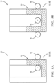
- the MMIC 12 includes an arrangement 14, see Figs. 5A and 5B , of solder-balls 16 configured to couple relatively high-frequency, e.g. greater than 10GHz, radar-signals into or out of the MMIC 12, which may be emitted and/or detected by the MMIC 12, which is not shown in Figs. 5A and 5B .
- the MMIC 12 may also input and output relatively low-frequency signals, e.g. less than 10MHz, that may be commonly called control-signals. Those control-signals may also be connected or propagated via other-solder-balls that may also be used to directly attach the MMIC 12 to a PCB.
- the assembly 10 includes a single printed-circuit-board 18 (PCB 18).
- PCB 18 printed-circuit-board 18
- the modifier 'single' is used to exclude or avoid or distinguish from radar-assembly designs and prior art with multiple circuit boards and/or multiple types of circuit boards, i.e. designs that used more than one type of dielectric materials for forming the substrates of the multiple circuit boards that may be layered together to form a unified circuit board.
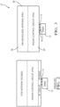
- Fig. 2 shows an example of multiple types (e.g. FR4 and RO3003 from Rogers Corporation) of circuit boards layered together.
- RO3003 is a known substrate material often used for high-frequency applications, e.g. radar, because of the dielectric properties, e.g.
- the PCB 18 of the radar assembly 10 described herein is advantageously formed of a single type of laminate-material, for example FR4, as shown in Fig. 3 .
- the modifier 'directly' is used to exclude or avoid or distinguish from designs and prior art that suggest using a small printed circuit board formed of high-frequency material (e.g. RO3003) between a relatively low-frequency circuit board and/or antenna-elements of the assembly 10 or the system.
- the assembly 10 includes at least one instance of an antenna-element 20 as shown in Fig. 4 , or may include multiple instances of the antenna-element 20 as shown in Fig. 1 .
- the antenna-element 20 may be characterize as integral with or integral to the PCB 18, i.e. is built into the PCB 18 or fabricated at the same time the PCB 18 is fabricated. Alternatively, it is contemplated that the antenna-element 20 could be formed of a separate sheet of formed (e.g. stamped/punched) metal or foil to define antenna-element 20.
- the antenna-element 20 includes, i.e. is configure to define, one or more radiation-slots 22 configured to couple radar-signals into the antenna-element from the surrounding environment (i.e. receive radar-signals), and/or out of the antenna-element into (i.e. broadcast radar-signals).
- the antenna-element 20 includes an air-waveguide, in particular, a ridge-air-waveguide 24 configured to propagate radar-signals to or from the one or more radiation-slots 22.
- the ridge-air-waveguide 24 has a U-shaped cross-section as shown in Figs. 8B and 8D .
- the U-shaped cross-section of the ridge-air-waveguide 24 is advantageously used so that the actual-width of the ridge-air-waveguide 24 (the width of the U) is small enough so the input/output ends of multiple instances of the antenna-element 20 can be arranged directly over the MMIC 12.
- the effective-width or the electrical-width of ridge-air-waveguide 24 is selected based on the wavelength of the radar-signals, where the effective-width or the electrical-width corresponds to the length of a line that defines the U. That is, the effective-width or the electrical-width of ridge-air-waveguide 24 is greater than the actual-width of the ridge-air-waveguide 24.
- the air-cavities that define the antenna-elements 20 may be formed by removing areas of the substrate 26, and then various surfaces including some or all of those created by the removal of areas of the substrate 26 are plated with, for example, copper to form, for example, the ridge-air-waveguide 24 and the radiation-slots 22 of the antenna-element 20.
- Figs. 8A, 8B, 8C, and 8D illustrate non-limiting examples of various structures, e.g. the ridge-air-waveguide 24 and the radiation-slots 22 formed by the plating with all other parts of the PCB 18 being removed. It is noted that only the metal plating is shown, and the material that forms the substrate 26 is not shown in Figs. 8A, 8B, 8C, and 8D .
- the PCB 18 includes a transition-feature 28 configured to couple radar-signals between the arrangement 14 of solder-balls 16 and the ridge-air-waveguide 24 of the antenna-element 20.
- the transition-feature 28 is an air-waveguide that is characterized as a slot, and the slot extends between the arrangement 14 of solder-balls 16 and the ridge-air-waveguide 24.
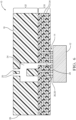
- Fig. 6 illustrates a non-limiting example of a sectional end-view of an embodiment of the assembly 10 that suggests the relationship between the transition-feature 28, the ridge-air-waveguide 24, and the radiation-slots 22.
- Fig. 5A shows a non-limiting example of part of the assembly 10 where the arrangement 14 of solder-balls 16 is characterized as a solder-ball-pair 14A. That two solder-balls are used is typically determined by the design or configuration of the radar-signal input/output of the MMIC 12.
- the transition-feature 28 it may be advantageous for the transition-feature 28 to be configured as or characterized as an L-shaped-slot.
- Figs. 7A, 7B, 7C, 7D, and 7E show various perspective views of the MMIC 12, the transition-feature 28 and the ridge-air-waveguide 24.
- Signals to/from the MMIC 12 are electromagnetically coupled to the transition-feature 28, which is an "L" shaped slot, to/from bottom of the transition-feature 28, and the upper side of the transition-feature 28 feeds the end of a ridge-air-waveguide 24.
- the end of the ridge part of the ridge-air-waveguide 24 is not touching the end wall of the ridge-air-waveguide 24.
- the topology of this transition makes it possible for the termination ends of the antenna-element 20 to be narrow enough to fit seven ridge air waveguides to the seven RF ports of the relatively small MMIC as shown in Fig. 1 .
- Fig. 5B shows a non-limiting example of part of the assembly 10 where the arrangement 14 of solder-balls 16 is characterized as a solder-ball-trio 14B.
- the arrangement 14 of solder-balls 16 is characterized as a solder-ball-trio 14B.
- that three solder-balls are used is generally determined by the design or configuration of the radar-signal input/output of the MMIC 12.
- the transition-feature 28 it may be advantageous for the transition-feature 28 to be configured as or characterized as a U-shaped-slot. Note that the end of the ridge part of the ridge-air-waveguide 24 is not touching the end wall of the ridge-air-waveguide 24.
- the radiation-slots 22 depicted in Figs. 8A-8D are opened on the top side or broad side of the ridge-air-waveguide 24, i.e. the top portion of an upside-down U, thereby forming what some refer to as an end-fed waveguide slot array antenna.
- the width of the ridge-air-waveguide 24 allows a radiator formed of multiple antenna-elements that is narrow enough to form an array without grating lobes.
- the cross section of the ridge-air-waveguide 24 can be individually optimized for transition and for radiator, a taper in between can bridge the two together.
- FIG. 1 illustrates a design example for radar-signals of 76.5GHz, where four receive antennas are separated by half wavelengths, and the three transmit antennas are separated by two and half wavelengths. Matching at the ports or radar-signal inputs/outputs of the MMIC is good, radiation pattern has a wide field of view in azimuth, and a 10deg beam width in elevation with side-lobe below -20dB, as shown in Figs 9A and 9B .
- the design is purposely selected for typical PCB fabrication processes and for minimal manufactural cost.
- the assembly 10 includes a monolithic-microwave-integrated-circuit 12 (MN ⁇ C 12), and a single printed-circuit-board 18 (PCB 18) formed of a single type of laminate-material and directly attached to the MMIC 12.
- the MMIC 12 includes an arrangement 14 of solder-balls 16 configured to couple radar-signals into or out of the MMIC 12.
- the PCB 18 includes a lower portion 30 adjacent to the MMIC 12 and an upper-portion 32 opposite the lower-portion 30 with respect to the MMIC 12.
- the upper-portion 32 includes an antenna-element 20 that includes one or more radiation-slots 22 configured to couple radar-signals into or out of the antenna-element 20, and a ridge-air-waveguide 24 configured to propagate radar-signals to or from the one or more radiation-slots 22.
- the lower-portion 30 includes one or more conductor-layers 34 configured to communicate one or more control-signals to the MMIC 12, and a transition-feature 28 configured to couple radar-signals between the arrangement 14 of solder-balls 16 and the ridge-air-waveguide 24.
- the transition-feature 28 is characterized as a slot that extends through the lower-portion 30 between the arrangement 14 of solder-balls 16 and the ridge-air-waveguide 24.
- the surfaces that define the ridge-air-waveguide 24 and the transition-feature 28 are plated with metal.
- a printed-circuit-board 18 for a radar assembly 10 is provided.
- the PCB 18 includes a substrate 26 formed of a single type of laminate-material, and an array 36 of solder-pads 38 on a surface of the substrate 26.
- the array 36 of solder-pads 38 is configured for making a direct connection to an arrangement 14 of solder-balls 16 of a monolithic-microwave-integrated-circuit 12 or MMIC 12.
- the arrangement 14 of solder-balls 16 configured to couple radar-signals into or out of the MMIC 12.
- the PCB 18 includes or defines a lower portion 30 adjacent to the solder-pads and an upper-portion 32 opposite the lower-portion 30 with respect to the solder-pads 38.
- the upper-portion 32 includes an antenna-element 20 that includes or defines one or more radiation-slots 22 configured to couple radar-signals into or out of the antenna-element 20, and a ridge-air-waveguide 24 configured to propagate radar-signals to or from the one or more radiation-slots 22.
- the lower portion 30 includes one or more conductor-layers 34 configured to communicate one or more control-signals to the MMIC 12, and a transition-feature 28 configured to couple radar-signals through the lower-layer between the arrangement 14 of solder-balls 16 and the ridge-air-waveguide 24.
- the transition-feature 28 is characterized as a slot that extends through the lower-portion 30 between the arrangement 14 of solder-balls 16 and the ridge-air-waveguide 24.
- the transition-feature 28 is preferably, i.e. is characterized as, an L-shaped-slot. If the arrangement 14 of solder-balls 16 is characterized as a solder-ball-trio 14B, then the transition-feature 28 is preferably, i.e. is characterized, as a U-shaped-slot. If dielectric material such as FR4 is used for the substrate 26, the air cavity surfaces that define the ridge-air-waveguide 24 and the transition-feature 28 and radiation-slots 22 may be plated with metal. However, plating is not necessary if the upper-portion 32 is built from formed/stamped metal foil.
- a radar assembly 10 (the assembly 10), and a printed-circuit-board 18 (PCB 18) are provided.
- the narrow air waveguides provided by the ridge-air-waveguide 24 in combination with a transition air wave guide provided or defined by the transition-feature 28 described herein result in a means to transmit and receive radar-signal with very little or no transmission losses, while being more economical to manufacture that prior radar assemblies.
- the assembly is designed/configured to be compatible with known printed circuit board fabrication processes.
Landscapes
- Engineering & Computer Science (AREA)
- Radar, Positioning & Navigation (AREA)
- Remote Sensing (AREA)
- Physics & Mathematics (AREA)
- Microelectronics & Electronic Packaging (AREA)
- Computer Networks & Wireless Communication (AREA)
- General Physics & Mathematics (AREA)
- Electromagnetism (AREA)
- Waveguide Aerials (AREA)
- Variable-Direction Aerials And Aerial Arrays (AREA)
- Radar Systems Or Details Thereof (AREA)
Claims (13)
- Ensemble radar (10) comprenant :un circuit intégré monolithique hyperfréquence (12) incluant un arrangement (14) de billes de soudure (16) configuré pour coupler des signaux radar dans ou hors du circuit intégré monolithique hyperfréquence (12) ;un élément d'antenne (20) qui inclut une ou plusieurs fentes de rayonnement (22) configurées pour coupler des signaux radar dans ou hors de l'élément d'antenne (20) et un guide d'ondes à air nervuré (24) configuré pour propager des signaux radar vers ou depuis lesdites une ou plusieurs fentes de rayonnement (22) ; etune carte de circuit imprimé unique (18) directement attachée au circuit intégré monolithique hyperfréquence (12), la carte de circuit imprimé unique (18) inclut une caractéristique de transition (28) configurée pour coupler des signaux radar entre l'arrangement (14) de billes de soudure (16) et le guide d'ondes à air nervuré (24), dans lequel la caractéristique de transition (28) est une fente qui s'étend entre l'arrangement (14) de billes de soudure (16) et le guide d'ondes à air nervuré (24), dans lequel, soit :l'arrangement (14) de billes de soudure (16) est une paire de billes de soudure (14A) et la caractéristique de transition (28) est une fente en forme de L ; soitl'arrangement (14) de billes de soudure (16) est un trio de billes de soudure (14B) et la caractéristique de transition (28) est une fente en forme de U.
- Ensemble (10) selon la revendication 1, dans lequel la carte de circuit imprimé unique (18) est formée d'un seul type de matériau stratifié.
- Ensemble (10) selon la revendication 2, dans lequel le type de matériau stratifié est FR-4.
- Ensemble (10) selon la revendication 2, dans lequel l'élément d'antenne (20) fait partie intégrante de la carte de circuit imprimé unique (18).
- Ensemble (10) selon l'une quelconque des revendications précédentes, dans lequel les surfaces qui définissent le guide d'ondes à air nervuré (24) et la caractéristique de transition (28) sont plaquées avec du métal.
- Ensemble (10) selon l'une quelconque des revendications précédentes, dans lequel l'ensemble (10) inclut d'autres billes de soudure (16) qui attachent directement le circuit intégré monolithique hyperfréquence (12) à la carte de circuit imprimé unique (18).
- Ensemble radar (10) comprenant :un circuit intégré monolithique hyperfréquence (12) incluant un arrangement (14) de billes de soudure (16) configuré pour coupler des signaux radar dans ou hors du circuit intégré monolithique hyperfréquence (12) ; etune carte de circuit imprimé unique (18) formée d'un seul type de matériau stratifié et directement attachée au circuit intégré monolithique hyperfréquence (12), la carte de circuit imprimé unique (18) inclut une partie inférieure (30) adjacente au circuit intégré monolithique hyperfréquence (12) et une partie supérieure (32) opposée à la partie inférieure (30) par rapport au circuit intégré monolithique hyperfréquence (12),la partie supérieure (32) inclut un élément d'antenne (20) qui inclut une ou plusieurs fentes de rayonnement (22) configurées pour coupler des signaux radar dans ou hors de l'élément d'antenne (20) et un guide d'ondes à air nervuré (24) configuré pour propager des signaux radar vers ou depuis lesdites une ou plusieurs fentes de rayonnement (22),la partie inférieure (30) inclut une ou plusieurs couches conductrices (34) configurées pour communiquer un ou plusieurs signaux de commande au circuit intégré monolithique hyperfréquence (12), etune caractéristique de transition (28) configurée pour coupler des signaux radar entre l'arrangement (14) de billes de soudure (16) et le guide d'ondes à air nervuré (24), dans lequel la caractéristique de transition (28) est une fente qui s'étend à travers la partie inférieure (30) entre l'arrangement (14) de billes de soudure (16) et le guide d'ondes à air nervuré (24), et les surfaces qui définissent le guide d'ondes à air nervuré (24) et la caractéristique de transition (28) sont plaquées avec du métal, dans lequel soit :l'arrangement (14) de billes de soudure (16) est une paire de billes de soudure (14A) et la caractéristique de transition (28) est une fente en forme de L ; soitl'arrangement (14) de billes de soudure (16) est un trio de billes de soudure (14B) et la caractéristique de transition (28) est une fente en forme de U.
- Ensemble (10) selon la revendication 7, dans lequel le type de matériau stratifié est FR-4.
- Ensemble (10) selon l'une quelconque des revendications 7 ou 8, dans lequel l'élément d'antenne (20) fait partie intégrante de la carte de circuit imprimé unique (18).
- Carte de circuit imprimé (18) pour un ensemble radar (10) comprenant :un substrat (26) formé d'un seul type de matériau stratifié ;un arrangement (14) de plots de soudure (38) sur une surface du substrat (26), ledit arrangement (14) de plots de soudure (38) étant configuré pour établir une connexion directe avec un arrangement (14) de billes de soudure (16) d'un circuit intégré monolithique hyperfréquence (12), ledit arrangement (14) de billes de soudure (16) étant configuré pour coupler des signaux radar dans ou hors du circuit intégré monolithique hyperfréquence (12) ;ladite carte de circuit imprimé (18) inclut une partie inférieure (30) adjacente aux plots de soudure (38) et une partie supérieure (32) opposée à la partie inférieure (30) par rapport aux plots de soudure (38),ladite partie supérieure (32) inclut un élément d'antenne (20) qui inclut une ou plusieurs fentes de rayonnement (22) configurées pour coupler des signaux radar dans ou hors de l'élément d'antenne (20) et un guide d'ondes à air nervuré (24) configuré pour propager des signaux radar vers ou depuis lesdites une ou plusieurs fentes de rayonnement (22),ladite partie inférieure (30) inclut une ou plusieurs couches conductrices (34) configurées pour communiquer un ou plusieurs signaux de commande au circuit intégré monolithique hyperfréquence (12) et une caractéristique de transition (28) configurée pour coupler des signaux radar à travers la couche inférieure entre l'arrangement (14) de billes de soudure (16) et le guide d'ondes à air nervuré (24), ladite caractéristique de transition (28) est une fente qui s'étend à travers la partie inférieure (30) entre l'arrangement (14) de billes de soudure (16) et le guide d'ondes à air nervuré (24), dans laquelle soit :l'arrangement (14) de billes de soudure (16) est une paire de billes de soudure (14A) et la caractéristique de transition (28) est une fente en forme de L ; soitl'arrangement (14) de billes de soudure (16) est un trio de billes de soudure (14B) et la caractéristique de transition (28) est une fente en forme de U.
- Carte de circuit imprimé (18) selon la revendication 10, dans laquelle les surfaces qui définissent le guide d'ondes à air nervuré (24) et la caractéristique de transition (28) sont plaquées avec du métal.
- Carte de circuit imprimé (18) selon l'une quelconque des revendications 10 ou 11, dans laquelle le type de matériau stratifié est FR-4.
- Carte de circuit imprimé (18) selon l'une quelconque des revendications 10 à 12, dans laquelle l'élément d'antenne (20) fait partie intégrante de la carte de circuit imprimé unique (18).
Applications Claiming Priority (2)
| Application Number | Priority Date | Filing Date | Title |
|---|---|---|---|
| US201862752130P | 2018-10-29 | 2018-10-29 | |
| US16/175,501 US11011816B2 (en) | 2018-10-29 | 2018-10-30 | Radar assembly with a slot transition through a printed circuit board |
Publications (2)
| Publication Number | Publication Date |
|---|---|
| EP3647807A1 EP3647807A1 (fr) | 2020-05-06 |
| EP3647807B1 true EP3647807B1 (fr) | 2023-12-13 |
Family
ID=68084605
Family Applications (1)
| Application Number | Title | Priority Date | Filing Date |
|---|---|---|---|
| EP19199951.5A Active EP3647807B1 (fr) | 2018-10-29 | 2019-09-26 | Ensemble radar doté d'une transition à fente par l'intermédiaire d'une carte de circuit imprimé |
Country Status (3)
| Country | Link |
|---|---|
| US (1) | US11011816B2 (fr) |
| EP (1) | EP3647807B1 (fr) |
| CN (1) | CN111123210B (fr) |
Families Citing this family (22)
| Publication number | Priority date | Publication date | Assignee | Title |
|---|---|---|---|---|
| DE102018203106A1 (de) * | 2018-03-01 | 2019-09-05 | Conti Temic Microelectronic Gmbh | Radarsystem zur Umfelderfassung eines Kraftfahrzeugs mit einer Kunststoffantenne |
| US11454720B2 (en) * | 2018-11-28 | 2022-09-27 | Magna Electronics Inc. | Vehicle radar system with enhanced wave guide antenna system |
| DE102020209307A1 (de) * | 2020-07-23 | 2022-01-27 | Robert Bosch Gesellschaft mit beschränkter Haftung | Radarsensor mit Hohlleiterstruktur |
| US20230268666A1 (en) * | 2020-07-28 | 2023-08-24 | Sensata Technologies, Inc. | Modular waveguide to printed circuit board interconnected radar design |
| US11749883B2 (en) | 2020-12-18 | 2023-09-05 | Aptiv Technologies Limited | Waveguide with radiation slots and parasitic elements for asymmetrical coverage |
| US11901601B2 (en) | 2020-12-18 | 2024-02-13 | Aptiv Technologies Limited | Waveguide with a zigzag for suppressing grating lobes |
| US12058804B2 (en) | 2021-02-09 | 2024-08-06 | Aptiv Technologies AG | Formed waveguide antennas of a radar assembly |
| US11962085B2 (en) | 2021-05-13 | 2024-04-16 | Aptiv Technologies AG | Two-part folded waveguide having a sinusoidal shape channel including horn shape radiating slots formed therein which are spaced apart by one-half wavelength |
| US11749884B2 (en) | 2021-05-17 | 2023-09-05 | HJWAVE Co., Ltd. | Multi-layer antenna structure supporting wide band and wide angle |
| US12355151B2 (en) | 2021-05-17 | 2025-07-08 | HJWAVE Co., Ltd. | Antenna structure with reduced angle error |
| US11616282B2 (en) | 2021-08-03 | 2023-03-28 | Aptiv Technologies Limited | Transition between a single-ended port and differential ports having stubs that match with input impedances of the single-ended and differential ports |
| EP4138215A1 (fr) * | 2021-08-20 | 2023-02-22 | GM Cruise Holdings LLC | Système de radar de balayage avec guides d'ondes intégrés à substrat et structures de dissipation de chaleur |
| US12230857B2 (en) | 2021-11-30 | 2025-02-18 | Navico, Inc. | Radar waveguide and choke assembly |
| US12456816B2 (en) * | 2022-05-02 | 2025-10-28 | Aptiv Technologies AG | Waveguide with slot antennas and reflectors |
| US12613334B2 (en) * | 2022-06-28 | 2026-04-28 | Magna Electronics, Llc | Integrated circuit to waveguide transitional structures and related sensor assemblies |
| US12451578B2 (en) | 2022-12-30 | 2025-10-21 | Nxp B.V. | Interposers with millimeter-wave coaxial-to-waveguide transistions |
| US12451579B2 (en) | 2022-12-30 | 2025-10-21 | Nxp B.V. | Interposers with millimeter-wave transitions |
| US12537308B2 (en) | 2023-01-24 | 2026-01-27 | Aptiv Technologies AG | Symmetrical two-piece waveguide |
| US12148992B2 (en) | 2023-01-25 | 2024-11-19 | Aptiv Technologies AG | Hybrid horn waveguide antenna |
| DE102023203759A1 (de) | 2023-04-24 | 2024-10-24 | Robert Bosch Gesellschaft mit beschränkter Haftung | Radarsensor mit mehreren Radarchipeinheiten |
| DE102023211697A1 (de) * | 2023-11-23 | 2025-05-28 | Continental Autonomous Mobility Germany GmbH | Wellenleiteranordnung, Radarsensor sowie Fahrzeug |
| US20260036670A1 (en) * | 2024-04-19 | 2026-02-05 | Aptiv Technologies AG | Innovative Open Waveguide Bend for Leakage Mitigation |
Citations (1)
| Publication number | Priority date | Publication date | Assignee | Title |
|---|---|---|---|---|
| EP1983614A1 (fr) * | 2006-02-06 | 2008-10-22 | Mitsubishi Electric Corporation | Module à haute fréquence |
Family Cites Families (12)
| Publication number | Priority date | Publication date | Assignee | Title |
|---|---|---|---|---|
| DE10300955B4 (de) | 2003-01-13 | 2005-10-27 | Epcos Ag | Radar-Transceiver für Mikrowellen- und Millimeterwellenanwendungen |
| JP2006253953A (ja) | 2005-03-09 | 2006-09-21 | Fujitsu Ltd | 通信用高周波モジュールおよびその製造方法 |
| US9196958B2 (en) * | 2012-07-26 | 2015-11-24 | Apple Inc. | Antenna structures and shield layers on packaged wireless circuits |
| US9620854B2 (en) * | 2013-01-09 | 2017-04-11 | Nxp Usa, Inc. | Electronic high frequency device and manufacturing method |
| CN110167255A (zh) * | 2013-03-15 | 2019-08-23 | 伟创力有限责任公司 | 用于创建完全微波吸收印刷电路板的方法和装置 |
| DE102014200660A1 (de) | 2014-01-16 | 2015-07-16 | Conti Temic Microelectronic Gmbh | Sende- und Empfangseinheit für Radarsignale und Verfahren zur Herstellung derselben |
| DE102016125419B4 (de) * | 2015-12-24 | 2022-10-20 | Nidec Elesys Corporation | Wellenleitervorrichtung, Schlitzantenne und Radar, Radarsystem sowie Drahtlos-Kommunikationssystem mit der Schlitzantenne |
| JP2019047141A (ja) * | 2016-03-29 | 2019-03-22 | 日本電産エレシス株式会社 | マイクロ波ic導波路装置モジュール、レーダ装置およびレーダシステム |
| DE112016006695B4 (de) * | 2016-04-01 | 2026-01-29 | Intel Corporation | Gehäuse auf Antennengehäuse und Verfahren zu dessen Herstellung |
| DE102016212129B4 (de) * | 2016-07-04 | 2022-05-19 | Schweizer Electronic Ag | Hochfrequenz-Sende-/Empfangselement und Verfahren zur Herstellung eines Hochfrequenz-Sende-/Empfangselementes |
| EP3364457A1 (fr) * | 2017-02-15 | 2018-08-22 | Nxp B.V. | Conditionnement de circuit intégré avec antenne |
| JP2018164252A (ja) * | 2017-03-24 | 2018-10-18 | 日本電産株式会社 | スロットアレーアンテナ、および当該スロットアレーアンテナを備えるレーダ |
-
2018
- 2018-10-30 US US16/175,501 patent/US11011816B2/en active Active
-
2019
- 2019-09-26 EP EP19199951.5A patent/EP3647807B1/fr active Active
- 2019-10-28 CN CN201911030880.6A patent/CN111123210B/zh active Active
Patent Citations (1)
| Publication number | Priority date | Publication date | Assignee | Title |
|---|---|---|---|---|
| EP1983614A1 (fr) * | 2006-02-06 | 2008-10-22 | Mitsubishi Electric Corporation | Module à haute fréquence |
Also Published As
| Publication number | Publication date |
|---|---|
| EP3647807A1 (fr) | 2020-05-06 |
| CN111123210B (zh) | 2023-09-05 |
| US20200136225A1 (en) | 2020-04-30 |
| US11011816B2 (en) | 2021-05-18 |
| CN111123210A (zh) | 2020-05-08 |
Similar Documents
| Publication | Publication Date | Title |
|---|---|---|
| EP3647807B1 (fr) | Ensemble radar doté d'une transition à fente par l'intermédiaire d'une carte de circuit imprimé | |
| US11604273B2 (en) | Radar system for detecting the environment of a motor vehicle having a plastic antenna | |
| US11536829B2 (en) | Vehicle radar system with radar embedded into radome | |
| EP3460903B1 (fr) | Dispositif d'antenne à entrée différentielle directe pouvant être utilisé sur un véhicule automatisé | |
| KR101621480B1 (ko) | 도파관 대 유전체 도파관의 천이 구조 | |
| US10141636B2 (en) | Volumetric scan automotive radar with end-fire antenna on partially laminated multi-layer PCB | |
| US12313767B2 (en) | Method for manufacturing a radar sensor | |
| EP1418643A2 (fr) | Réseau d'antennes microruban à filtres périodiques | |
| CA2397748A1 (fr) | Cornet d'antenne et procedes associes | |
| EP3220475B1 (fr) | Dispositif de signalisation comprenant un substrat de guide d'ondes intégré | |
| US11515624B2 (en) | Integrated cavity backed slot array antenna system | |
| US11552379B2 (en) | Transition from a stripline to a waveguide | |
| KR20150125262A (ko) | 다층 기판 및 다층 기판의 제조 방법 | |
| CN114914672A (zh) | 雷达组件的成形波导天线 | |
| CN103098301B (zh) | 具有设置在多个平面内的天线元件的平面组合天线 | |
| EP4130783A1 (fr) | Système de radar pour véhicule | |
| US20190348740A1 (en) | Transmission line-waveguide transition device | |
| US11011814B2 (en) | Coupling comprising a conductive wire embedded in a post-wall waveguide and extending into a hollow tube waveguide | |
| CN118285019A (zh) | 雷达传感器及制造方法 | |
| CN217306728U (zh) | 功分器、天线装置、无线电器件以及设备 | |
| US7224239B2 (en) | Structural element having a coplanar line | |
| US11621464B2 (en) | Waveguide assembly | |
| KR20240058150A (ko) | 도파관 구조를 갖는 레이더 센서 | |
| EP3937308B1 (fr) | Ensemble d'antennes | |
| CN117117483A (zh) | 天线结构、毫米波雷达及可移动设备 |
Legal Events
| Date | Code | Title | Description |
|---|---|---|---|
| PUAI | Public reference made under article 153(3) epc to a published international application that has entered the european phase |
Free format text: ORIGINAL CODE: 0009012 |
|
| STAA | Information on the status of an ep patent application or granted ep patent |
Free format text: STATUS: THE APPLICATION HAS BEEN PUBLISHED |
|
| AK | Designated contracting states |
Kind code of ref document: A1 Designated state(s): AL AT BE BG CH CY CZ DE DK EE ES FI FR GB GR HR HU IE IS IT LI LT LU LV MC MK MT NL NO PL PT RO RS SE SI SK SM TR |
|
| AX | Request for extension of the european patent |
Extension state: BA ME |
|
| STAA | Information on the status of an ep patent application or granted ep patent |
Free format text: STATUS: REQUEST FOR EXAMINATION WAS MADE |
|
| 17P | Request for examination filed |
Effective date: 20201105 |
|
| RBV | Designated contracting states (corrected) |
Designated state(s): AL AT BE BG CH CY CZ DE DK EE ES FI FR GB GR HR HU IE IS IT LI LT LU LV MC MK MT NL NO PL PT RO RS SE SI SK SM TR |
|
| STAA | Information on the status of an ep patent application or granted ep patent |
Free format text: STATUS: EXAMINATION IS IN PROGRESS |
|
| 17Q | First examination report despatched |
Effective date: 20220331 |
|
| RAP3 | Party data changed (applicant data changed or rights of an application transferred) |
Owner name: APTIV TECHNOLOGIES LIMITED |
|
| GRAP | Despatch of communication of intention to grant a patent |
Free format text: ORIGINAL CODE: EPIDOSNIGR1 |
|
| STAA | Information on the status of an ep patent application or granted ep patent |
Free format text: STATUS: GRANT OF PATENT IS INTENDED |
|
| INTG | Intention to grant announced |
Effective date: 20230905 |
|
| GRAS | Grant fee paid |
Free format text: ORIGINAL CODE: EPIDOSNIGR3 |
|
| GRAA | (expected) grant |
Free format text: ORIGINAL CODE: 0009210 |
|
| STAA | Information on the status of an ep patent application or granted ep patent |
Free format text: STATUS: THE PATENT HAS BEEN GRANTED |
|
| AK | Designated contracting states |
Kind code of ref document: B1 Designated state(s): AL AT BE BG CH CY CZ DE DK EE ES FI FR GB GR HR HU IE IS IT LI LT LU LV MC MK MT NL NO PL PT RO RS SE SI SK SM TR |
|
| REG | Reference to a national code |
Ref country code: GB Ref legal event code: FG4D |
|
| REG | Reference to a national code |
Ref country code: CH Ref legal event code: EP |
|
| P01 | Opt-out of the competence of the unified patent court (upc) registered |
Effective date: 20231113 |
|
| REG | Reference to a national code |
Ref country code: DE Ref legal event code: R096 Ref document number: 602019043141 Country of ref document: DE |
|
| REG | Reference to a national code |
Ref country code: IE Ref legal event code: FG4D |
|
| PG25 | Lapsed in a contracting state [announced via postgrant information from national office to epo] |
Ref country code: GR Free format text: LAPSE BECAUSE OF FAILURE TO SUBMIT A TRANSLATION OF THE DESCRIPTION OR TO PAY THE FEE WITHIN THE PRESCRIBED TIME-LIMIT Effective date: 20240314 |
|
| REG | Reference to a national code |
Ref country code: LT Ref legal event code: MG9D |
|
| PG25 | Lapsed in a contracting state [announced via postgrant information from national office to epo] |
Ref country code: LT Free format text: LAPSE BECAUSE OF FAILURE TO SUBMIT A TRANSLATION OF THE DESCRIPTION OR TO PAY THE FEE WITHIN THE PRESCRIBED TIME-LIMIT Effective date: 20231213 |
|
| REG | Reference to a national code |
Ref country code: NL Ref legal event code: MP Effective date: 20231213 |
|
| PG25 | Lapsed in a contracting state [announced via postgrant information from national office to epo] |
Ref country code: ES Free format text: LAPSE BECAUSE OF FAILURE TO SUBMIT A TRANSLATION OF THE DESCRIPTION OR TO PAY THE FEE WITHIN THE PRESCRIBED TIME-LIMIT Effective date: 20231213 |
|
| PG25 | Lapsed in a contracting state [announced via postgrant information from national office to epo] |
Ref country code: LT Free format text: LAPSE BECAUSE OF FAILURE TO SUBMIT A TRANSLATION OF THE DESCRIPTION OR TO PAY THE FEE WITHIN THE PRESCRIBED TIME-LIMIT Effective date: 20231213 Ref country code: GR Free format text: LAPSE BECAUSE OF FAILURE TO SUBMIT A TRANSLATION OF THE DESCRIPTION OR TO PAY THE FEE WITHIN THE PRESCRIBED TIME-LIMIT Effective date: 20240314 Ref country code: ES Free format text: LAPSE BECAUSE OF FAILURE TO SUBMIT A TRANSLATION OF THE DESCRIPTION OR TO PAY THE FEE WITHIN THE PRESCRIBED TIME-LIMIT Effective date: 20231213 Ref country code: BG Free format text: LAPSE BECAUSE OF FAILURE TO SUBMIT A TRANSLATION OF THE DESCRIPTION OR TO PAY THE FEE WITHIN THE PRESCRIBED TIME-LIMIT Effective date: 20240313 |
|
| REG | Reference to a national code |
Ref country code: AT Ref legal event code: MK05 Ref document number: 1640891 Country of ref document: AT Kind code of ref document: T Effective date: 20231213 |
|
| PG25 | Lapsed in a contracting state [announced via postgrant information from national office to epo] |
Ref country code: NL Free format text: LAPSE BECAUSE OF FAILURE TO SUBMIT A TRANSLATION OF THE DESCRIPTION OR TO PAY THE FEE WITHIN THE PRESCRIBED TIME-LIMIT Effective date: 20231213 |
|
| PG25 | Lapsed in a contracting state [announced via postgrant information from national office to epo] |
Ref country code: SE Free format text: LAPSE BECAUSE OF FAILURE TO SUBMIT A TRANSLATION OF THE DESCRIPTION OR TO PAY THE FEE WITHIN THE PRESCRIBED TIME-LIMIT Effective date: 20231213 Ref country code: RS Free format text: LAPSE BECAUSE OF FAILURE TO SUBMIT A TRANSLATION OF THE DESCRIPTION OR TO PAY THE FEE WITHIN THE PRESCRIBED TIME-LIMIT Effective date: 20231213 Ref country code: NO Free format text: LAPSE BECAUSE OF FAILURE TO SUBMIT A TRANSLATION OF THE DESCRIPTION OR TO PAY THE FEE WITHIN THE PRESCRIBED TIME-LIMIT Effective date: 20240313 Ref country code: NL Free format text: LAPSE BECAUSE OF FAILURE TO SUBMIT A TRANSLATION OF THE DESCRIPTION OR TO PAY THE FEE WITHIN THE PRESCRIBED TIME-LIMIT Effective date: 20231213 Ref country code: LV Free format text: LAPSE BECAUSE OF FAILURE TO SUBMIT A TRANSLATION OF THE DESCRIPTION OR TO PAY THE FEE WITHIN THE PRESCRIBED TIME-LIMIT Effective date: 20231213 Ref country code: HR Free format text: LAPSE BECAUSE OF FAILURE TO SUBMIT A TRANSLATION OF THE DESCRIPTION OR TO PAY THE FEE WITHIN THE PRESCRIBED TIME-LIMIT Effective date: 20231213 |
|
| PG25 | Lapsed in a contracting state [announced via postgrant information from national office to epo] |
Ref country code: IS Free format text: LAPSE BECAUSE OF FAILURE TO SUBMIT A TRANSLATION OF THE DESCRIPTION OR TO PAY THE FEE WITHIN THE PRESCRIBED TIME-LIMIT Effective date: 20240413 |
|
| PG25 | Lapsed in a contracting state [announced via postgrant information from national office to epo] |
Ref country code: AT Free format text: LAPSE BECAUSE OF FAILURE TO SUBMIT A TRANSLATION OF THE DESCRIPTION OR TO PAY THE FEE WITHIN THE PRESCRIBED TIME-LIMIT Effective date: 20231213 Ref country code: CZ Free format text: LAPSE BECAUSE OF FAILURE TO SUBMIT A TRANSLATION OF THE DESCRIPTION OR TO PAY THE FEE WITHIN THE PRESCRIBED TIME-LIMIT Effective date: 20231213 |
|
| PG25 | Lapsed in a contracting state [announced via postgrant information from national office to epo] |
Ref country code: SK Free format text: LAPSE BECAUSE OF FAILURE TO SUBMIT A TRANSLATION OF THE DESCRIPTION OR TO PAY THE FEE WITHIN THE PRESCRIBED TIME-LIMIT Effective date: 20231213 |
|
| PG25 | Lapsed in a contracting state [announced via postgrant information from national office to epo] |
Ref country code: SM Free format text: LAPSE BECAUSE OF FAILURE TO SUBMIT A TRANSLATION OF THE DESCRIPTION OR TO PAY THE FEE WITHIN THE PRESCRIBED TIME-LIMIT Effective date: 20231213 Ref country code: SK Free format text: LAPSE BECAUSE OF FAILURE TO SUBMIT A TRANSLATION OF THE DESCRIPTION OR TO PAY THE FEE WITHIN THE PRESCRIBED TIME-LIMIT Effective date: 20231213 Ref country code: RO Free format text: LAPSE BECAUSE OF FAILURE TO SUBMIT A TRANSLATION OF THE DESCRIPTION OR TO PAY THE FEE WITHIN THE PRESCRIBED TIME-LIMIT Effective date: 20231213 Ref country code: IT Free format text: LAPSE BECAUSE OF FAILURE TO SUBMIT A TRANSLATION OF THE DESCRIPTION OR TO PAY THE FEE WITHIN THE PRESCRIBED TIME-LIMIT Effective date: 20231213 Ref country code: IS Free format text: LAPSE BECAUSE OF FAILURE TO SUBMIT A TRANSLATION OF THE DESCRIPTION OR TO PAY THE FEE WITHIN THE PRESCRIBED TIME-LIMIT Effective date: 20240413 Ref country code: EE Free format text: LAPSE BECAUSE OF FAILURE TO SUBMIT A TRANSLATION OF THE DESCRIPTION OR TO PAY THE FEE WITHIN THE PRESCRIBED TIME-LIMIT Effective date: 20231213 Ref country code: CZ Free format text: LAPSE BECAUSE OF FAILURE TO SUBMIT A TRANSLATION OF THE DESCRIPTION OR TO PAY THE FEE WITHIN THE PRESCRIBED TIME-LIMIT Effective date: 20231213 Ref country code: AT Free format text: LAPSE BECAUSE OF FAILURE TO SUBMIT A TRANSLATION OF THE DESCRIPTION OR TO PAY THE FEE WITHIN THE PRESCRIBED TIME-LIMIT Effective date: 20231213 |
|
| PG25 | Lapsed in a contracting state [announced via postgrant information from national office to epo] |
Ref country code: PL Free format text: LAPSE BECAUSE OF FAILURE TO SUBMIT A TRANSLATION OF THE DESCRIPTION OR TO PAY THE FEE WITHIN THE PRESCRIBED TIME-LIMIT Effective date: 20231213 Ref country code: PT Free format text: LAPSE BECAUSE OF FAILURE TO SUBMIT A TRANSLATION OF THE DESCRIPTION OR TO PAY THE FEE WITHIN THE PRESCRIBED TIME-LIMIT Effective date: 20240415 |
|
| PG25 | Lapsed in a contracting state [announced via postgrant information from national office to epo] |
Ref country code: PT Free format text: LAPSE BECAUSE OF FAILURE TO SUBMIT A TRANSLATION OF THE DESCRIPTION OR TO PAY THE FEE WITHIN THE PRESCRIBED TIME-LIMIT Effective date: 20240415 Ref country code: PL Free format text: LAPSE BECAUSE OF FAILURE TO SUBMIT A TRANSLATION OF THE DESCRIPTION OR TO PAY THE FEE WITHIN THE PRESCRIBED TIME-LIMIT Effective date: 20231213 |
|
| REG | Reference to a national code |
Ref country code: DE Ref legal event code: R097 Ref document number: 602019043141 Country of ref document: DE |
|
| PG25 | Lapsed in a contracting state [announced via postgrant information from national office to epo] |
Ref country code: DK Free format text: LAPSE BECAUSE OF FAILURE TO SUBMIT A TRANSLATION OF THE DESCRIPTION OR TO PAY THE FEE WITHIN THE PRESCRIBED TIME-LIMIT Effective date: 20231213 |
|
| PLBE | No opposition filed within time limit |
Free format text: ORIGINAL CODE: 0009261 |
|
| STAA | Information on the status of an ep patent application or granted ep patent |
Free format text: STATUS: NO OPPOSITION FILED WITHIN TIME LIMIT |
|
| PG25 | Lapsed in a contracting state [announced via postgrant information from national office to epo] |
Ref country code: SI Free format text: LAPSE BECAUSE OF FAILURE TO SUBMIT A TRANSLATION OF THE DESCRIPTION OR TO PAY THE FEE WITHIN THE PRESCRIBED TIME-LIMIT Effective date: 20231213 |
|
| PG25 | Lapsed in a contracting state [announced via postgrant information from national office to epo] |
Ref country code: SI Free format text: LAPSE BECAUSE OF FAILURE TO SUBMIT A TRANSLATION OF THE DESCRIPTION OR TO PAY THE FEE WITHIN THE PRESCRIBED TIME-LIMIT Effective date: 20231213 Ref country code: DK Free format text: LAPSE BECAUSE OF FAILURE TO SUBMIT A TRANSLATION OF THE DESCRIPTION OR TO PAY THE FEE WITHIN THE PRESCRIBED TIME-LIMIT Effective date: 20231213 |
|
| 26N | No opposition filed |
Effective date: 20240916 |
|
| PG25 | Lapsed in a contracting state [announced via postgrant information from national office to epo] |
Ref country code: MC Free format text: LAPSE BECAUSE OF FAILURE TO SUBMIT A TRANSLATION OF THE DESCRIPTION OR TO PAY THE FEE WITHIN THE PRESCRIBED TIME-LIMIT Effective date: 20231213 |
|
| REG | Reference to a national code |
Ref country code: DE Ref legal event code: R081 Ref document number: 602019043141 Country of ref document: DE Owner name: APTIV TECHNOLOGIES AG, CH Free format text: FORMER OWNER: APTIV TECHNOLOGIES LIMITED, ST. MICHAEL, BB Ref country code: CH Ref legal event code: PL |
|
| PG25 | Lapsed in a contracting state [announced via postgrant information from national office to epo] |
Ref country code: LU Free format text: LAPSE BECAUSE OF NON-PAYMENT OF DUE FEES Effective date: 20240926 |
|
| REG | Reference to a national code |
Ref country code: BE Ref legal event code: MM Effective date: 20240930 |
|
| PG25 | Lapsed in a contracting state [announced via postgrant information from national office to epo] |
Ref country code: BE Free format text: LAPSE BECAUSE OF NON-PAYMENT OF DUE FEES Effective date: 20240930 |
|
| PG25 | Lapsed in a contracting state [announced via postgrant information from national office to epo] |
Ref country code: CH Free format text: LAPSE BECAUSE OF NON-PAYMENT OF DUE FEES Effective date: 20240930 |
|
| PG25 | Lapsed in a contracting state [announced via postgrant information from national office to epo] |
Ref country code: IE Free format text: LAPSE BECAUSE OF NON-PAYMENT OF DUE FEES Effective date: 20240926 |
|
| PG25 | Lapsed in a contracting state [announced via postgrant information from national office to epo] |
Ref country code: FI Free format text: LAPSE BECAUSE OF FAILURE TO SUBMIT A TRANSLATION OF THE DESCRIPTION OR TO PAY THE FEE WITHIN THE PRESCRIBED TIME-LIMIT Effective date: 20231213 |
|
| PGFP | Annual fee paid to national office [announced via postgrant information from national office to epo] |
Ref country code: DE Payment date: 20250814 Year of fee payment: 7 |
|
| PGFP | Annual fee paid to national office [announced via postgrant information from national office to epo] |
Ref country code: GB Payment date: 20250924 Year of fee payment: 7 |
|
| PGFP | Annual fee paid to national office [announced via postgrant information from national office to epo] |
Ref country code: FR Payment date: 20250908 Year of fee payment: 7 |
|
| PG25 | Lapsed in a contracting state [announced via postgrant information from national office to epo] |
Ref country code: CY Free format text: LAPSE BECAUSE OF FAILURE TO SUBMIT A TRANSLATION OF THE DESCRIPTION OR TO PAY THE FEE WITHIN THE PRESCRIBED TIME-LIMIT; INVALID AB INITIO Effective date: 20190926 |
|
| PG25 | Lapsed in a contracting state [announced via postgrant information from national office to epo] |
Ref country code: HU Free format text: LAPSE BECAUSE OF FAILURE TO SUBMIT A TRANSLATION OF THE DESCRIPTION OR TO PAY THE FEE WITHIN THE PRESCRIBED TIME-LIMIT; INVALID AB INITIO Effective date: 20190926 |