EP1988144A1 - Substance d'élément électroluminescent organique, élément électroluminescent organique, dispositif d'affichage et dispositif d'éclairage - Google Patents
Substance d'élément électroluminescent organique, élément électroluminescent organique, dispositif d'affichage et dispositif d'éclairage Download PDFInfo
- Publication number
- EP1988144A1 EP1988144A1 EP07707404A EP07707404A EP1988144A1 EP 1988144 A1 EP1988144 A1 EP 1988144A1 EP 07707404 A EP07707404 A EP 07707404A EP 07707404 A EP07707404 A EP 07707404A EP 1988144 A1 EP1988144 A1 EP 1988144A1
- Authority
- EP
- European Patent Office
- Prior art keywords
- group
- organic electroluminescent
- electroluminescent element
- organic
- layer
- Prior art date
- Legal status (The legal status is an assumption and is not a legal conclusion. Google has not performed a legal analysis and makes no representation as to the accuracy of the status listed.)
- Withdrawn
Links
- 0 CC(C=C(C(*(S1)=CCC2)=CC2=C)S1=C1)C1=* Chemical compound CC(C=C(C(*(S1)=CCC2)=CC2=C)S1=C1)C1=* 0.000 description 20
- DTETYCNJKAUROO-UHFFFAOYSA-N CC(C(O1)=O)NC1=O Chemical compound CC(C(O1)=O)NC1=O DTETYCNJKAUROO-UHFFFAOYSA-N 0.000 description 1
- YCSFMOVBARTLBW-UHFFFAOYSA-N CCOCCC(C(O)=O)N Chemical compound CCOCCC(C(O)=O)N YCSFMOVBARTLBW-UHFFFAOYSA-N 0.000 description 1
- PBAAWSSCVKWHMH-UHFFFAOYSA-N CN1C=CN(C)C1N Chemical compound CN1C=CN(C)C1N PBAAWSSCVKWHMH-UHFFFAOYSA-N 0.000 description 1
- YSWBFLWKAIRHEI-UHFFFAOYSA-N Cc1c(C)nc[nH]1 Chemical compound Cc1c(C)nc[nH]1 YSWBFLWKAIRHEI-UHFFFAOYSA-N 0.000 description 1
- QBEBPBHFVLKPPO-UHFFFAOYSA-N Cc1c(CSc2ccc(C)cc2)c2ccccc2[s]1 Chemical compound Cc1c(CSc2ccc(C)cc2)c2ccccc2[s]1 QBEBPBHFVLKPPO-UHFFFAOYSA-N 0.000 description 1
- BFIMMTCNYPIMRN-UHFFFAOYSA-N Cc1cc(C)c(C)c(C)c1 Chemical compound Cc1cc(C)c(C)c(C)c1 BFIMMTCNYPIMRN-UHFFFAOYSA-N 0.000 description 1
- YXTVGHKRJZPQQH-UHFFFAOYSA-N Nc1c(C=O)c(Cl)c(C=[U+])[nH]1 Chemical compound Nc1c(C=O)c(Cl)c(C=[U+])[nH]1 YXTVGHKRJZPQQH-UHFFFAOYSA-N 0.000 description 1
Images

Classifications
-
- H—ELECTRICITY
- H10—SEMICONDUCTOR DEVICES; ELECTRIC SOLID-STATE DEVICES NOT OTHERWISE PROVIDED FOR
- H10K—ORGANIC ELECTRIC SOLID-STATE DEVICES
- H10K85/00—Organic materials used in the body or electrodes of devices covered by this subclass
- H10K85/30—Coordination compounds
- H10K85/341—Transition metal complexes, e.g. Ru(II)polypyridine complexes
- H10K85/342—Transition metal complexes, e.g. Ru(II)polypyridine complexes comprising iridium
-
- C—CHEMISTRY; METALLURGY
- C07—ORGANIC CHEMISTRY
- C07F—ACYCLIC, CARBOCYCLIC OR HETEROCYCLIC COMPOUNDS CONTAINING ELEMENTS OTHER THAN CARBON, HYDROGEN, HALOGEN, OXYGEN, NITROGEN, SULFUR, SELENIUM OR TELLURIUM
- C07F15/00—Compounds containing elements of Groups 8, 9, 10 or 18 of the Periodic Table
- C07F15/0006—Compounds containing elements of Groups 8, 9, 10 or 18 of the Periodic Table compounds of the platinum group
- C07F15/0033—Iridium compounds
-
- C—CHEMISTRY; METALLURGY
- C09—DYES; PAINTS; POLISHES; NATURAL RESINS; ADHESIVES; COMPOSITIONS NOT OTHERWISE PROVIDED FOR; APPLICATIONS OF MATERIALS NOT OTHERWISE PROVIDED FOR
- C09K—MATERIALS FOR MISCELLANEOUS APPLICATIONS, NOT PROVIDED FOR ELSEWHERE
- C09K11/00—Luminescent materials, e.g. electroluminescent or chemiluminescent
- C09K11/06—Luminescent materials, e.g. electroluminescent or chemiluminescent containing organic luminescent materials
-
- H—ELECTRICITY
- H10—SEMICONDUCTOR DEVICES; ELECTRIC SOLID-STATE DEVICES NOT OTHERWISE PROVIDED FOR
- H10K—ORGANIC ELECTRIC SOLID-STATE DEVICES
- H10K85/00—Organic materials used in the body or electrodes of devices covered by this subclass
- H10K85/10—Organic polymers or oligomers
- H10K85/141—Organic polymers or oligomers comprising aliphatic or olefinic chains, e.g. poly N-vinylcarbazol, PVC or PTFE
-
- C—CHEMISTRY; METALLURGY
- C09—DYES; PAINTS; POLISHES; NATURAL RESINS; ADHESIVES; COMPOSITIONS NOT OTHERWISE PROVIDED FOR; APPLICATIONS OF MATERIALS NOT OTHERWISE PROVIDED FOR
- C09K—MATERIALS FOR MISCELLANEOUS APPLICATIONS, NOT PROVIDED FOR ELSEWHERE
- C09K2211/00—Chemical nature of organic luminescent or tenebrescent compounds
- C09K2211/10—Non-macromolecular compounds
- C09K2211/1003—Carbocyclic compounds
- C09K2211/1007—Non-condensed systems
-
- C—CHEMISTRY; METALLURGY
- C09—DYES; PAINTS; POLISHES; NATURAL RESINS; ADHESIVES; COMPOSITIONS NOT OTHERWISE PROVIDED FOR; APPLICATIONS OF MATERIALS NOT OTHERWISE PROVIDED FOR
- C09K—MATERIALS FOR MISCELLANEOUS APPLICATIONS, NOT PROVIDED FOR ELSEWHERE
- C09K2211/00—Chemical nature of organic luminescent or tenebrescent compounds
- C09K2211/10—Non-macromolecular compounds
- C09K2211/1003—Carbocyclic compounds
- C09K2211/1011—Condensed systems
-
- C—CHEMISTRY; METALLURGY
- C09—DYES; PAINTS; POLISHES; NATURAL RESINS; ADHESIVES; COMPOSITIONS NOT OTHERWISE PROVIDED FOR; APPLICATIONS OF MATERIALS NOT OTHERWISE PROVIDED FOR
- C09K—MATERIALS FOR MISCELLANEOUS APPLICATIONS, NOT PROVIDED FOR ELSEWHERE
- C09K2211/00—Chemical nature of organic luminescent or tenebrescent compounds
- C09K2211/10—Non-macromolecular compounds
- C09K2211/1018—Heterocyclic compounds
- C09K2211/1025—Heterocyclic compounds characterised by ligands
- C09K2211/1029—Heterocyclic compounds characterised by ligands containing one nitrogen atom as the heteroatom
-
- C—CHEMISTRY; METALLURGY
- C09—DYES; PAINTS; POLISHES; NATURAL RESINS; ADHESIVES; COMPOSITIONS NOT OTHERWISE PROVIDED FOR; APPLICATIONS OF MATERIALS NOT OTHERWISE PROVIDED FOR
- C09K—MATERIALS FOR MISCELLANEOUS APPLICATIONS, NOT PROVIDED FOR ELSEWHERE
- C09K2211/00—Chemical nature of organic luminescent or tenebrescent compounds
- C09K2211/10—Non-macromolecular compounds
- C09K2211/1018—Heterocyclic compounds
- C09K2211/1025—Heterocyclic compounds characterised by ligands
- C09K2211/1029—Heterocyclic compounds characterised by ligands containing one nitrogen atom as the heteroatom
- C09K2211/1033—Heterocyclic compounds characterised by ligands containing one nitrogen atom as the heteroatom with oxygen
-
- C—CHEMISTRY; METALLURGY
- C09—DYES; PAINTS; POLISHES; NATURAL RESINS; ADHESIVES; COMPOSITIONS NOT OTHERWISE PROVIDED FOR; APPLICATIONS OF MATERIALS NOT OTHERWISE PROVIDED FOR
- C09K—MATERIALS FOR MISCELLANEOUS APPLICATIONS, NOT PROVIDED FOR ELSEWHERE
- C09K2211/00—Chemical nature of organic luminescent or tenebrescent compounds
- C09K2211/10—Non-macromolecular compounds
- C09K2211/1018—Heterocyclic compounds
- C09K2211/1025—Heterocyclic compounds characterised by ligands
- C09K2211/1029—Heterocyclic compounds characterised by ligands containing one nitrogen atom as the heteroatom
- C09K2211/1037—Heterocyclic compounds characterised by ligands containing one nitrogen atom as the heteroatom with sulfur
-
- C—CHEMISTRY; METALLURGY
- C09—DYES; PAINTS; POLISHES; NATURAL RESINS; ADHESIVES; COMPOSITIONS NOT OTHERWISE PROVIDED FOR; APPLICATIONS OF MATERIALS NOT OTHERWISE PROVIDED FOR
- C09K—MATERIALS FOR MISCELLANEOUS APPLICATIONS, NOT PROVIDED FOR ELSEWHERE
- C09K2211/00—Chemical nature of organic luminescent or tenebrescent compounds
- C09K2211/10—Non-macromolecular compounds
- C09K2211/1018—Heterocyclic compounds
- C09K2211/1025—Heterocyclic compounds characterised by ligands
- C09K2211/1044—Heterocyclic compounds characterised by ligands containing two nitrogen atoms as heteroatoms
-
- C—CHEMISTRY; METALLURGY
- C09—DYES; PAINTS; POLISHES; NATURAL RESINS; ADHESIVES; COMPOSITIONS NOT OTHERWISE PROVIDED FOR; APPLICATIONS OF MATERIALS NOT OTHERWISE PROVIDED FOR
- C09K—MATERIALS FOR MISCELLANEOUS APPLICATIONS, NOT PROVIDED FOR ELSEWHERE
- C09K2211/00—Chemical nature of organic luminescent or tenebrescent compounds
- C09K2211/10—Non-macromolecular compounds
- C09K2211/1018—Heterocyclic compounds
- C09K2211/1025—Heterocyclic compounds characterised by ligands
- C09K2211/1059—Heterocyclic compounds characterised by ligands containing three nitrogen atoms as heteroatoms
-
- C—CHEMISTRY; METALLURGY
- C09—DYES; PAINTS; POLISHES; NATURAL RESINS; ADHESIVES; COMPOSITIONS NOT OTHERWISE PROVIDED FOR; APPLICATIONS OF MATERIALS NOT OTHERWISE PROVIDED FOR
- C09K—MATERIALS FOR MISCELLANEOUS APPLICATIONS, NOT PROVIDED FOR ELSEWHERE
- C09K2211/00—Chemical nature of organic luminescent or tenebrescent compounds
- C09K2211/10—Non-macromolecular compounds
- C09K2211/1018—Heterocyclic compounds
- C09K2211/1025—Heterocyclic compounds characterised by ligands
- C09K2211/1074—Heterocyclic compounds characterised by ligands containing more than three nitrogen atoms as heteroatoms
-
- C—CHEMISTRY; METALLURGY
- C09—DYES; PAINTS; POLISHES; NATURAL RESINS; ADHESIVES; COMPOSITIONS NOT OTHERWISE PROVIDED FOR; APPLICATIONS OF MATERIALS NOT OTHERWISE PROVIDED FOR
- C09K—MATERIALS FOR MISCELLANEOUS APPLICATIONS, NOT PROVIDED FOR ELSEWHERE
- C09K2211/00—Chemical nature of organic luminescent or tenebrescent compounds
- C09K2211/10—Non-macromolecular compounds
- C09K2211/1018—Heterocyclic compounds
- C09K2211/1025—Heterocyclic compounds characterised by ligands
- C09K2211/1088—Heterocyclic compounds characterised by ligands containing oxygen as the only heteroatom
-
- C—CHEMISTRY; METALLURGY
- C09—DYES; PAINTS; POLISHES; NATURAL RESINS; ADHESIVES; COMPOSITIONS NOT OTHERWISE PROVIDED FOR; APPLICATIONS OF MATERIALS NOT OTHERWISE PROVIDED FOR
- C09K—MATERIALS FOR MISCELLANEOUS APPLICATIONS, NOT PROVIDED FOR ELSEWHERE
- C09K2211/00—Chemical nature of organic luminescent or tenebrescent compounds
- C09K2211/10—Non-macromolecular compounds
- C09K2211/1018—Heterocyclic compounds
- C09K2211/1025—Heterocyclic compounds characterised by ligands
- C09K2211/1092—Heterocyclic compounds characterised by ligands containing sulfur as the only heteroatom
-
- C—CHEMISTRY; METALLURGY
- C09—DYES; PAINTS; POLISHES; NATURAL RESINS; ADHESIVES; COMPOSITIONS NOT OTHERWISE PROVIDED FOR; APPLICATIONS OF MATERIALS NOT OTHERWISE PROVIDED FOR
- C09K—MATERIALS FOR MISCELLANEOUS APPLICATIONS, NOT PROVIDED FOR ELSEWHERE
- C09K2211/00—Chemical nature of organic luminescent or tenebrescent compounds
- C09K2211/14—Macromolecular compounds
- C09K2211/1441—Heterocyclic
-
- C—CHEMISTRY; METALLURGY
- C09—DYES; PAINTS; POLISHES; NATURAL RESINS; ADHESIVES; COMPOSITIONS NOT OTHERWISE PROVIDED FOR; APPLICATIONS OF MATERIALS NOT OTHERWISE PROVIDED FOR
- C09K—MATERIALS FOR MISCELLANEOUS APPLICATIONS, NOT PROVIDED FOR ELSEWHERE
- C09K2211/00—Chemical nature of organic luminescent or tenebrescent compounds
- C09K2211/14—Macromolecular compounds
- C09K2211/1441—Heterocyclic
- C09K2211/145—Heterocyclic containing oxygen as the only heteroatom
-
- C—CHEMISTRY; METALLURGY
- C09—DYES; PAINTS; POLISHES; NATURAL RESINS; ADHESIVES; COMPOSITIONS NOT OTHERWISE PROVIDED FOR; APPLICATIONS OF MATERIALS NOT OTHERWISE PROVIDED FOR
- C09K—MATERIALS FOR MISCELLANEOUS APPLICATIONS, NOT PROVIDED FOR ELSEWHERE
- C09K2211/00—Chemical nature of organic luminescent or tenebrescent compounds
- C09K2211/14—Macromolecular compounds
- C09K2211/1441—Heterocyclic
- C09K2211/1466—Heterocyclic containing nitrogen as the only heteroatom
-
- C—CHEMISTRY; METALLURGY
- C09—DYES; PAINTS; POLISHES; NATURAL RESINS; ADHESIVES; COMPOSITIONS NOT OTHERWISE PROVIDED FOR; APPLICATIONS OF MATERIALS NOT OTHERWISE PROVIDED FOR
- C09K—MATERIALS FOR MISCELLANEOUS APPLICATIONS, NOT PROVIDED FOR ELSEWHERE
- C09K2211/00—Chemical nature of organic luminescent or tenebrescent compounds
- C09K2211/18—Metal complexes
- C09K2211/185—Metal complexes of the platinum group, i.e. Os, Ir, Pt, Ru, Rh or Pd
-
- H—ELECTRICITY
- H10—SEMICONDUCTOR DEVICES; ELECTRIC SOLID-STATE DEVICES NOT OTHERWISE PROVIDED FOR
- H10K—ORGANIC ELECTRIC SOLID-STATE DEVICES
- H10K2101/00—Properties of the organic materials covered by group H10K85/00
- H10K2101/10—Triplet emission
-
- H—ELECTRICITY
- H10—SEMICONDUCTOR DEVICES; ELECTRIC SOLID-STATE DEVICES NOT OTHERWISE PROVIDED FOR
- H10K—ORGANIC ELECTRIC SOLID-STATE DEVICES
- H10K50/00—Organic light-emitting devices
- H10K50/10—OLEDs or polymer light-emitting diodes [PLED]
- H10K50/11—OLEDs or polymer light-emitting diodes [PLED] characterised by the electroluminescent [EL] layers
-
- H—ELECTRICITY
- H10—SEMICONDUCTOR DEVICES; ELECTRIC SOLID-STATE DEVICES NOT OTHERWISE PROVIDED FOR
- H10K—ORGANIC ELECTRIC SOLID-STATE DEVICES
- H10K85/00—Organic materials used in the body or electrodes of devices covered by this subclass
- H10K85/30—Coordination compounds
- H10K85/321—Metal complexes comprising a group IIIA element, e.g. Tris (8-hydroxyquinoline) gallium [Gaq3]
- H10K85/324—Metal complexes comprising a group IIIA element, e.g. Tris (8-hydroxyquinoline) gallium [Gaq3] comprising aluminium, e.g. Alq3
-
- H—ELECTRICITY
- H10—SEMICONDUCTOR DEVICES; ELECTRIC SOLID-STATE DEVICES NOT OTHERWISE PROVIDED FOR
- H10K—ORGANIC ELECTRIC SOLID-STATE DEVICES
- H10K85/00—Organic materials used in the body or electrodes of devices covered by this subclass
- H10K85/60—Organic compounds having low molecular weight
- H10K85/649—Aromatic compounds comprising a hetero atom
- H10K85/657—Polycyclic condensed heteroaromatic hydrocarbons
- H10K85/6572—Polycyclic condensed heteroaromatic hydrocarbons comprising only nitrogen in the heteroaromatic polycondensed ring system, e.g. phenanthroline or carbazole
-
- Y—GENERAL TAGGING OF NEW TECHNOLOGICAL DEVELOPMENTS; GENERAL TAGGING OF CROSS-SECTIONAL TECHNOLOGIES SPANNING OVER SEVERAL SECTIONS OF THE IPC; TECHNICAL SUBJECTS COVERED BY FORMER USPC CROSS-REFERENCE ART COLLECTIONS [XRACs] AND DIGESTS
- Y02—TECHNOLOGIES OR APPLICATIONS FOR MITIGATION OR ADAPTATION AGAINST CLIMATE CHANGE
- Y02B—CLIMATE CHANGE MITIGATION TECHNOLOGIES RELATED TO BUILDINGS, e.g. HOUSING, HOUSE APPLIANCES OR RELATED END-USER APPLICATIONS
- Y02B20/00—Energy efficient lighting technologies, e.g. halogen lamps or gas discharge lamps
Definitions
- the present invention relates to an organic electroluminescent element material, an organic electroluminescent element, a display device and an illumination device.
- an emission type electronic display device includes an electroluminescence display (hereinafter, referred to as an ELD).
- ELD electroluminescence display
- a constituent element of ELD includes such as an inorganic electroluminescent element and an organic electroluminescent element (hereinafter, referred to as an organic EL element).
- An inorganic electroluminescent element has been utilized as a flat light source, however, requires a high voltage of alternating current to operate an emission element.
- An organic electroluminescent element is an element provided with a constitution comprising an emission layer containing a emitting substance being sandwiched with a cathode and an anode, and an exciton is generated by an electron and a positive hole being injected into the emission layer to be recombined, resulting emission utilizing light release (fluorescence ⁇ phosphorescence) at the time of deactivation of said exciton; the emission is possible at a voltage of approximately a few to a few tens volts, and an organic electroluminescent element is attracting attention with respect to such as superior viewing angle and high visual recognition due to a self-emission type as well as space saving and portability due to a completely solid element of a thin layer type.
- JP-A 63-264692 JP-A refers to Japanese Patent Publication Open to Public Inspection No.
- JP-A 3-255190 an element having an organic emission layer comprising a 8-hydroxyquinoline aluminum complex as a host compound which is doped with quinacridone type dye
- Ikai et al. at The 10th International Workshops on Inorganic and Organic Electroluminescence (EL'00, Hamamatsu) utilized a hole transporting compound as a host of a phosphorescent compound.
- EL'00 Inorganic and Organic Electroluminescence
- M. E. Tompson et al. utilized various types of electron transporting materials as a host of a phosphorescent compound doped with a new iridium complex.
- emission luminance and emission efficiency are significantly improved compared to conventional elements because the emitting light arises from phosphorescence, however, there has been a problem of a poor emission life of the element compared to conventional elements. It is hard to achieve an emission of a short wavelength and an improvement of an emission life of the element for a phosphorescent emission material provided with a high efficiency. At present state, it cannot be achieved a level of a practical use.
- a ligand known are metal complexes having phenylpyrazole in which the phenyl group undergoes substitution (refer, for example, to Patent Documents 1 and 2).
- substitution mode of the phenyl group of phenylpyrazole which is disclosed in the above, the lifetime of the luminescent element is improved but is still insufficient. Further, in view of luminescent efficiency, much room for improvement still remains.
- ligands having a substituent exhibiting steric hindrance are appropriate for improvement of luminance, and there are examples of application to the phenylpyrazole mother nucleus (refer, for example, to Patent Document 3).
- Patent Documents 4, 5, and 7 Examples of metal complexes, in which phenylimidazole as a ligand is employed as a basic skeleton, are disclosed (refer, for example, to Patent Documents 4, 5, and 7).
- described is luminescent wavelength, driving characteristics of the elements, external quantum efficiency, and chromaticity, but not specifically described is the lifetime of the luminescent elements.
- This invention has been made in view of these problems, and an object of this invention is to provide an organic EL element material with a controlled emission wavelength which have high emission efficiency and long emission life, an illumination device and a display device by utilizing said element material.
- This invention has enabled to provide an organic EL element material for and an organic EL element having specific properties, and it has been achieved to provide an organic EL element, an illumination device and a display device having high emission efficiency and long emission life utilizing said organic EL element material.
- an organic EL element material which is a metal complex having a specific ligand, could be obtained by adopting a constitution defined by any one of the embodiments of the present invention described any one of claims 1-9.
- An organic EL element having high emission efficiency and long emission life could be obtained by utilizing said organic EL element material.
- the display device described above and the illumination device described above each, exhibit high luminance as well as high durability, could be obtained.
- the inventors of the present invention conducted further diligent investigation and also discovered that with regard to phenylimidazole derivatives, the stability of the complex varied to a great extent depending on effects of the substitution position and types of a substituent to phenylimidazole employed as a mother nucleus, whereby the above significantly affected the luminescent lifetime.
- the inventors of the present invention discovered that as the metal complexes according to the present invention, by introducing a substituent having a specific steric or electronic parameter for imidazole into a heterocyclic ring, an aromatic heterocyclic ring, or an aromatic hydrocarbon ring, luminescent lifetime was markedly extended, which had caused problems for the organic EL element prepared by employing an organic EL element material which controlled the luminescent wavelength to the shorter wavelength side only by conventional metal complexes for blue, especially by an electron attractive group, whereby compatibility of the luminescent efficiency and the luminescent lifetime was realized.
- the inventors of the present invention conducted diligent investigation and achieved the present invention by discovering the following effects via introduction of a cyclic substituent having a bulky substituent in the ortho position onto the N position of phenylimidazole;
- the partial structure represented in parenthesis having m1 or the partial structure represented by the tautomer is called a primary ligand, while the partial structure represented in parenthesis having m2 or the tautomer is called a secondary ligand.
- the above metal complexes are composed of a primary ligand or its tautomer as well as a secondary ligand or its tautomer.
- m2 0 is allowed, namely all the ligands of the above metal complexes are composed of only the partial structure represented by the primary ligand or its tautomers.
- ligands also called coordination compounds
- ligands also called coordination compounds
- the ligand in complexes is composed of 1 or 2 types, but is preferably composed of only one type.
- Ligands employed in conventional metal complexes known in the art include various types. Examples include ligands (for example, halogen ligands, being preferably a chlorine ligand, and nitrogen containing heterocyclic ligands such as bipyridyl or phenanthroline, and diketone ligands) described, for example, in H. Yersin, "Photochemistry and Photophysics of Coordination Compounds” Springer-Verlag Co., published in 1987 , and in Akio Yamamoto, "Yuki Kinzoku Kagaku -Kiso to Oyo- (Organic Metal Chemistry -Bases and Applications-)” Shokabo Sha, published in 1982 .
- ligands for example, halogen ligands, being preferably a chlorine ligand, and nitrogen containing heterocyclic ligands such as bipyridyl or phenanthroline, and diketone ligands
- transition metal elements also simply referred to as transition metals
- iridium and platinum are listed as a preferable transition metal element.
- organic EL element materials which exhibit high luminescent efficiency and long luminescent lifetime, a lighting device and a display device.
- a layer incorporating the metal complexes represented by above Formulas (1), (2), (3) or (4) according to the present invention, or Formula (4) is an emission layer and/or an electron inhibition layer. Further, when incorporated in the emission layer, by employing them as a emission dopant in the emission layer, it is possible to achieve an increase in the quantum efficiency (to realize high luminance) to be taken out and the extension of luminescent lifetime of the organic EL elements of the present invention.
- Z represents a hydrocarbon ring or a heterocyclic ring (including each of the tautomers) in which a substituent of a steric parameter (being an Es value) of at most -0.5 is bound to at least one atom located in the third position from the nitrogen atom to be bound.
- Es value refers to a steric parameter derived from chemical reactivity. It is possible to describe that a decrease in this value indicates that the substituent becomes spatially more bulky -
- Es value will now be described. It is common knowledge that in a hydrolysis reaction of esters under acidic conditions, effects for the progress of the reaction may be considered to be only caused by the steric hindrance. Based on this, the value which numerically expresses the steric hindrance is Es value.
- Es value of substituent X may be obtainable as follows.
- Reaction rate constant kX of the following chemical reaction in which ⁇ -position mono-substituted acetate, which is derived from ⁇ -position mono-substituted acetic acid prepared by substituting one hydrogen atom of the methyl group of acetic acid with substituent X, undergoes hydrolysis under acidic conditions, is obtained.
- Reaction rate constant kH of the following reaction (RX is the same as RY) in which acetate corresponding to the above ⁇ -position mono-substituted acetate undergoes hydrolysis under acetic conditions, is also obtained.
- Es log (kX/kH)
- reaction rate decreases due to steric hindrance of substituent X.
- Es value commonly becomes negative.
- two reaction rate constants namely kX and kH, are determined and it is calculated based on the above formula.
- Es value is detailed in Unger, S. H., Hansch, C., Prog . Phys. Org. Chem. 12, 91 (1976 ). Further, specific numerical values are also described in " Yakubutsu no Kozo Kassei Sokan (Structural Activity correlation)” (Kagaku no Ryoiki Zokan No. 122, Nanko Do), and "American Chemical Society Professional Reference Book, 'Exploring QSAR' p. 81, Table 3-3 ". Table 1 below shows some of them.
- the Es value which is defined in the present invention, is not determined while a methyl group is 0, but is determined while a hydrogen atom to be 0, whereby the Es value of the present invention is a value which is obtained by subtracting 1.24 from the Es value determined while a methyl group is 0.
- the Es value is commonly at most -0.5, is preferably between -7.0 and -0.6, but is most preferably between -7.0 and -1.0.
- a substituent at a steric parameter (being a Es value) of at most -0.5 for example, in the case in which keto-enol tautomers are present in R and R', the Es value of the keto portion is determined via conversion as an enol isomer. In cases in which other tautomers are present, Es values are determined based on the same conversion method. Further, a substituent at an Es value of at most -0.5 is preferably an electron donative group in terms of electronic effects.
- a substituent is electron donating means that Hammett ⁇ p value described below is a negative value and such substituent has a larger tendency to donate electrons to the bonded atoms when compared with a
- an electron-donating substituent include: a hydroxyl group, a methoxy group, an acetyloxy group, an amino group, a dimethylamino group, an acetylamino group, alkyl groups (for example, a methyl group, an ethyl group, a propyl group and tert-butyl) and aryl groups (for example, a phenyl group).
- alkyl groups for example, a methyl group, an ethyl group, a propyl group and tert-butyl
- aryl groups for example, a phenyl group.
- Hammett ⁇ p value of the present invention represents Hammett substituent constant ⁇ p.
- Hammett ⁇ p value was determined from the electronic effect of the substituent exerted on hydrolysis of ethyl benzoate by Hammett et al. Groups shown in, for example, " Structure-activity relationship of a drug" (Nankodo Co., Ltd.: 1979 ), or substituent Constants for Correlation Analysis in chemistry and biology" (C. Hansch and A.Leo, John Wiley&Sons, New York, 1979 ) can be cited.
- Examples of a cyclic hydrocarbon group in Formula (1) and having a steric parameter (Es) of -0.5 or less are a non-aromatic cyclic hydrocarbon group and an aromatic cyclic hydrocarbon group.
- Examples of non-aromatic cyclic hydrocarbon groups are a cyclopropyl group, a cyclopentyl group and a cyclohexyl group. These groups may have a substituent which will be described later.
- aromatic cyclic hydrocarbon groups are, a phenyl group, a p-chlorophenyl group, a mesityl group, a tolyl group, a xylyl group, a naphtyl group, an anthryl group, an azulenyl group, an acenaphthenyl group, a phenanthryl group, an indenyl group, a pyrenyl group, and a biphenyl group. These groups may have a substituent which will be described later.
- Examples of a heterocyclic group in Formula (1) and having a steric parameter (Es) of -0.5 or less are a non-aromatic heterocyclic group and an aromatic heterocyclic group.
- non-aromatic heterocyclic groups are, an epoxy group, an aziridinyl group, a thiiranyl group, an oxetanyl ting, an azethidinyl group, a thiethanyl group, a tetrohydrofuranyl group, a dioxoranyl group, a pyrrolidinyl group, a pyrrazolidinyl group, an imodazolidinyl group, an oxazolidinyl group, a tetrahydrothiophenyl group, a sulfolanyl group, a thiazolidinyl group, ⁇ -caprolactonyl group, ⁇ -caprolactam group, a piperidinyl group, a hexa
- aromatic heterocyclic groups are, a pyridyl group, a pyrimidinyl group, a furyl group, a pyrrolyl group, an imidazolyl group, a benzimidazolyl group, a pyrazolyl group, a piradinyl group, a triazolyl group (for example, a 1,2,4-triazole-1-yl group and a 1,2,3-triazole-1-yl group), an oxazolyl group, a benzoxazolyl group, a thiazolyl group, an isooxazolyl group, an isothiazolyl group, a furazanyl group, a thienyl group, a quinolyl group, a benzofuryl group, a dibenzofuryl group, a benzothienyl group, a dibenzothienyl group, an indolyl group, a carbazolyl group, a carbo
- These groups may have a substituent.
- the cyclic hydrocarbon group and the heterocyclic group having a steric parameter (Es) of -05. or less may have further a substituent. Examples of such substituents are the same as described for R 01 and R 02 in Formula (1).
- Z in Formula (1) Preferred examples of Z in Formula (1) are listed below. Other than the listed examples below, Z may have substituent(s), whereby Z is not limited to these examples. Incidentally, * represents a binding position.
- Y represents a carbon atom or a nitrogen atom, but is preferably a carbon atom.
- nitrogen-containing heterocyclic groups incorporating Y include a 2-imidazoyl group, a 2-(1,3,4-triazolyl) group, a 2-(1,3,5-triazolyl) group, and a 2-tetrazolyl group. Of these nitrogen-containing heterocyclic groups, the 2-imidazolyl group is most preferred.
- R 01 and R 02 each represents a hydrogen atom or a substituent.
- substituents include an alkyl group (for example, a methyl group, an ethyl group, a propyl group, an isopropyl group, a tert-butyl group, a pentyl group, a hexyl group, an octyl group, a dodecyl group, a tridecyl group, a tetradecyl group, and a pentadecyl group), a cycloalkyl group (for example, a cyclopentyl group and a cyclohexyl group), an alkenyl group (for example, a vinyl group and an allyl group), an alkynyl group (for example, an ethynyl group and a propargyl group), an aromatic hydrocarbon ring group (also called an aromatic carbon ring group or an aryl group such as a phenyl
- X represents either a carbon atom or a nitrogen atom, but is preferably a carbon atom.
- the hydrocarbon ring represented by A-C-X is an aromatic hydrocarbon ring, it is one in which one hydrogen atom at an optional position is removed from the 4n + 2 ⁇ based aromatic hydrocarbon compound, and specific examples include a phenyl group, a 1-naphthyl group, a 2-naphthyl group, a 9-anthryl group, a 1-anthryl group, a 9-phenanthryl group, a 2-triphenylenyl group, and a 3-perylenyl group.
- hydrocarbon ring group may be substituted, for example with the substituent described in R 01 , and further, may form a condensed ring (for example, a 9-pyrenyl group which is prepared by condensing a hydrocarbon ring to a 9-phenanthryl group or a 8-quinolyl group which is prepared by condensing a heterocycle to a phenyl group).
- a condensed ring for example, a 9-pyrenyl group which is prepared by condensing a hydrocarbon ring to a 9-phenanthryl group or a 8-quinolyl group which is prepared by condensing a heterocycle to a phenyl group.
- the heterocyclic group represented by A-C-X
- the heterocyclic group is an aromatic heterocyclic group
- at least one side contacting position of the portion bound to the nitrogen-containing aromatic heterocycle is a carbon atom, and though no particular limitation is made for the 4n + 2 ⁇ based aromatic group, both contacting positions of the portion bound to the nitrogen-containing aromatic heterocycle are carbon atoms.
- a 3-pyridyl group a 5-pyrimidyl group, a 4-pyridadyl group, a 5-pyridadyl group, a 4-isooxazolyl group, a 4-isothiazolyl group, a 4-pyrazolyl group, a 3-pyrrolo group, a 3-furyl group, and a 3-thienyl group.
- the above heterocycle may be substitutes, for example, with the substituent described in R 01 , and still further, may form a condensed ring.
- X 1 -L1-X 2 represents a bidentate ligand, and X 1 and X 2 each independently represents a carbon atom, a nitrogen atom, or an oxygen atom.
- L1 represents a group of atoms which forms a bidentate ligand together with X 2 .
- Specific examples of the bidentate ligand represented by X 1 -L1-X 2 include substituted or unsubstituted phenylpyridine, phenylpyrazole, phenylimidazole, phenyltriazole, phenyltetrazole, pyrazabole, acetylacetone, and picolinic acid.
- "ml" represents an integer of 1, 2, or 3, while m2 represents an integer of 0, 1, or 2, wherein m1 plus m2 is 2 or 3. Of these, the case in which m2 is 0 is preferred.
- R represents a substituent at a steric parameter (Es value) of at most -0.5, which is located in the ortho position of the ring composed of Z 2 bound to the nitrogen atom of the imidazole ring.
- Es values are as detailed in Formula (1).
- Specific examples of R include substituents shown in Table 1 in the description of Formula (1).
- R 1 represents a hydrogen atom or a substituent
- n1 represents an integer of 1 - 4.
- R 2 represents a hydrogen atom or a substituent and n2 represents an integer of 1 or 2.
- Z 2 represents a hydrocarbon ring or a heterocycle, or a group of atoms which is necessary to form a tautomer thereof.
- a cyclic hydrocarbon group represented by Z 2 is a non-aromatic cyclic hydrocarbon group or an aromatic cyclic hydrocarbon group.
- non-aromatic cyclic hydrocarbon groups are a cyclopropyl group, a cyclopentyl group and a cyclohexyl group.
- the above groups may further have a substituent, and examples of the substituents are the groups as defined for R 01 and R 02 of Formula (1).
- aromatic cyclic hydrocarbon groups are, a phenyl group, a biphenyl group, a naphthalennyl group, an azulenyl group, an anthracenyl group, a phenathrenyl group, a pyrenyl group, a chrysene group, a naphthacenyl group, a triphenylenyl group, o-terphyenylene, m-terphyenylene, p-terphyenylene, a acenaphtenyl group, a coronenyl group, a fluorenyl group, a fluoanthrenyl group, a naphthacenyl group, a pentacene group, a perirenyl group, pentaphenyl group, a picenyl group, a pyrenyl group, a pyranthrenyl group, an an an organic radicalsulfonyl group, a
- the above groups may further have a substituent, and examples of the substituents are the groups as defined for R 01 and R 02 of Formula (1).
- a heterocyclic group represented by Z 2 includes a non-aromatic heterocyclic group and an aromatic heterocyclic group.
- non-aromatic heterocyclic groups are, an epoxy group, an aziridinyl group, a thiiranyl group, an oxetanyl ting, an azethidinyl group, a thiethanyl group, a tetrohydrofuranyl group, a dioxoranyl group, a pyrrolidinyl group, a pyrrazolidinyl group, an imodazolidinyl group, an oxazolidinyl group, a tetrahydrothiophenyl group, a sulfolanyl group, a thiazolidinyl group, ⁇ -caprolactonyl group, ⁇ -caprolactam group, a piperidinyl group, a hexahydropyridazinyl group, a hex
- examples of aromatic heterocyclic groups represented by Z 2 are, a furanyl group, a thiophene group, an oxazole group, a pyrrolyl group, a pyridyl group, a pyridazinyl group, a pyrimidinyl group, a pyrazinyl group, a triazinyl group, a benzimidazolyl group, an oxadiazolyl group, a triazolyl group, an imidazolyl group, a pyrazolyl group, a thiazolyl group, an indazolyl group, a benzimidazolyl group, a benzothiazolyl group, a benzoxazolyl group, a quinoxalyl group, a quinazolinyl group, a phtharazinyl group, a carbazolyl group, a carbolinyl group, a diazacarbazoyl group (which
- the plurality of substituents may be bound together other to form a ring.
- Z 1 represents a group of atoms having divalence, which is necessary to form a 5- to 6-membered hydrocarbon ring or heterocycle together with C-C.
- Preferred as the hydrocarbon rings are aromatic hydrocarbon rings, while preferred as heterocycles are aromatic heterocycles.
- the aromatic hydrocarbon group having divalence is one in which two hydrogen atoms at an optional position are removed from a 4n + 2 based aromatic hydrocarbon compound, and specific examples include a group derived from a benzene group, a naphthalene group, an anthracene group, a phenathrene group, a triphenylene group, or a perirene group.
- the above aromatic hydrocarbon group having divalence may further have a substituent described for R 01 in Formula (1). And further, they may form a condensed ring.
- Aromatic heterocyclic groups having divalence are not particularly limited as long as at least one side contacting position of the portion bound to a nitrogen-containing heterocycle is a carbon atom and the above groups are 4n + 2 ⁇ based aromatic substituents, but dual side contacting positions of the portion bound to the nitrogen-containing aromatic heterocycle are carbon atoms.
- aromatic heterocyclic groups having divalence are groups derived from, a pyridyl group, a pyrimidinyl group, a pyridazinyl group, a isooxazolyl group, a isothiazolyl group, a pyrazolyl group, a pyrrolyl group, a furyl group, and a thiophenyl group.
- the above aromatic heterocycle having divalence may further be substituted with the substituent described in R 01 of Formula (1), and may further form a condensed ring.
- R 1 and R 2 each represents a hydrogen atom or a substituent, while n1 represents an integer of 1 - 4 and n2 represents an integer of 1 - 2.
- R 1 and R 2 each may be the same or different. Further, a plurality of substituents of R 1 or R 2 may be bound together to form a ring.
- X 1 -L1-X 2 represents a bidentate ligand, and X 1 and X 2 each independently represents a carbon atom, a nitrogen atom, or an oxygen atom.
- L1 represents a group of atoms which forms a bidentate ligand together with X 2 .
- Specific examples of the bidentate ligand represented by X 1 -L1-X 2 include substituted or unsubstituted phenylpyridine, phenylpyrazole, phenylimidazole, phenyltriazole, phenyltetrazole, pyrazabole, acetylacetone, and picolinic acid.
- "m1" represents an integer of 1, 2, or 3, while m2 represents an integer of 0, 1, or 2, wherein m1 plus m2 is 2 or 3. Of these, the case in which m2 is 0 is preferred.
- R represents a substituent at a steric parameter (Es value) of at most -0.5. Es values are as detailed in Formula (1). Specific examples of R include substituents shown in Table 1 in the description of Formula (1).
- R 1 and R 2 each represents a hydrogen atom or a substituent, and is defined as the description in Formula (2).
- R 3 represents a hydrogen atom or a substituent, while n3 represents an integer of 1 - 4. However, when a plurality of substituents is present, each R 3 may be the same or different. Further, a plurality of R 3 may be bound together to form a ring.
- X 1 -L1-X 2 represents a bidentate ligand, and X 1 and X 2 each independently represents a carbon atom, a nitrogen atom, or an oxygen atoms.
- L1 represents a group of atoms which forms a bidentate ligand together with X 2 .
- Specific examples of the bidentate ligand represented by X 1 -L1-X 2 are as those described in Formula (2).
- "m1" represents an integer of 1, 2, or 3, while m2 represents an integer of 0, 1, or 2, wherein m1 plus m2 is 2 or 3. Of these, the case in which m2 is 0 is preferred.
- R represents a substituent at a steric parameter (Es value) of at most -0.5. Es values are as detailed in Formula (1). Specific examples of R include substituents shown in Table 1 in the description of Formula (1).
- R 1 and R 2 each represents a hydrogen atom or a substituent, and is defined as the description in Formula (2).
- R 3 represents a hydrogen atom or a substituent, while n3 represents an integer of 1 - 4. However, when a plurality of substituent R 3 is present, each R 3 may be the same or different. Further, a plurality of R 3 may be bound together to form a ring.
- X 1 -L1-X 2 represents a bidentate ligand, and X 1 and X 2 each independently represents a carbon atom, a nitrogen atom, or an oxygen atom.
- L1 represents a group of atoms which forms a bidentate ligand together with X 2 .
- Specific examples of the bidentate ligand represented by X 1 -L1-X 2 are as those described in Formula (2).
- "m1" represents an integer of 1, 2, or 3, while m2 represents an integer of 0, 1, or 2, wherein m1 plus m2 is 2 or 3. Of these, the case in which m2 is 0 is preferred.
- R and R' are preferably electron donative groups.
- the electron donative groups are as those described in Formula (1).
- central metal M 1 represents a metal in Groups 8 - 10 of the periodical table of elements. Of these, iridium or platinum is particularly preferred.
- Metal complexes according to an organic EL element material of this invention can be synthesized by applying a method described in such as Organic Letter, vol. 3, No. 16, pp. 2579 - 2581 (2001 ), Inorganic Chemistry vol. 30, No. 8, pp. 1685 - 1687 (1991 ), J. Am. Chem. Soc., vol. 123, p. 4304 (2001 ), Inorganic Chemistry vol. 40, No. 7, pp. 1704 - 1711 (2001 ), Inorganic Chemistry vol. 41, No. 12, pp. 3055 - 3066 (2002 ), New Journal of Chemistry, vol. 26, p.1171 (2002 ), European Journal of Organic Chemistry Vol. 4, pp. 95 - 709 (12004 ), and reference documents described in these documents.
- said material is preferably utilized in an emission layer or an electron inhibition layer among constituent layers (details will be described later) of the organic EL element. Further, the material is preferably utilized as an emission dopant in an emission layer as described above.
- a mixing ratio of an emission dopant against an emission host as a primary component in an emission layer is preferably adjusted to a range of 0.1 - 30 weight%.
- plural types of compounds may be utilized in combination as an emission dopant, and the partner to be mixed may be a metal complex having a different structure, and a phosphorescent dopant or a fluorescent dopant having other structures.
- a dopant such as a phosphorescent dopant and a fluorescent dopant
- a metal complex employed as an emission dopant will be described.
- An emission dopant is roughly classified into two types, that is, a fluorescent dopant which emits fluorescence and a phosphorescent dopant which emits phosphorescence.
- a typical example of the former includes coumarin type dye, pyran type dye, cyanine type dye, chroconium type dye, squalium type dye, oxobenzanthracene type dye, fluorescein type dye, rhodamine type dye, pyrylium type dye, perylene type dye, stilbene type dye, polythiophene type dye or rare earth complex type fluorescent substances,
- a typical example of the latter (a phosphorescent dopant) is preferably a complex type compound containing metal of the 8th - 10th groups of the periodic table, more preferably an iridium compound and an osmium compound and most preferable among them is an iridium compound.
- a host compound, employed in the present invention refers to a compound, among those incorporated in the emission layer, which results in a phosphorescent quantum yield of less than 0.01 during emitting phosphorescence.
- Structures of the emission host employed in the present invention are not particularly limited.
- Representative compounds include those having a basic skeleton such as carbazole derivatives, triarylamine derivatives, aromatic borane derivatives, nitrogen-containing heterocyclic compounds, thiophene derivatives, furan derivatives, or oligoarylene compounds, or derivatives having a ring structure in which at least one of the carbon atoms of the hydrocarbon ring, which constitutes carboline derivatives and the carboline ring of the above carboline derivatives, is substituted with a nitrogen atom.
- a basic skeleton such as carbazole derivatives, triarylamine derivatives, aromatic borane derivatives, nitrogen-containing heterocyclic compounds, thiophene derivatives, furan derivatives, or oligoarylene compounds, or derivatives having a ring structure in which at least one of the carbon atoms of the hydrocarbon ring, which constitutes carboline derivatives and the carboline ring of the above carboline derivatives, is substituted
- derivatives are preferably employed which have a structure in which at least one carbon atom of carbazole derivatives, and carboline derivatives, and the hydrocarbon ring constituting the carboline ring of the above carboline derivatives.
- emission hosts will now be listed, however the present invention is not limited thereto. It is also preferable to employ these compounds as a positive hole inhibition material.
- prior art host compounds may be employed in combinations of a plurality of types.
- the use of a plurality of host compounds enables regulation of migration of electrons to make organic EL elements more efficient.
- Preferred as these prior art host compounds are those which exhibit positive hole transportability and electron transportability, minimize the variation of luminescent wavelength to a longer wavelength, and attain a high Tg (being a glass transition temperature).
- an emission host of this invention may be either a low molecular weight compound or a polymer compound having a repeating unit, in addition to a low molecular weight compound provided with a polymerizing group such as a vinyl group and an epoxy group (an evaporation polymerizing emission host).
- An emission host is preferably a compound having a positive hole transporting ability and an electron transporting ability, as well as preventing elongation of an emission wavelength and having a high Tg (a glass transition temperature).
- an emission host compounds described in the following Documents are preferable: For example, JP-A Nos. 2001-257076 , 2002-308855 , 2001-313179 , 2002-319491 , 2001-357977 , 2002-334786 , 2002-8860 , 2002-334787 , 2002-15871 , 2002-334788 , 2002-43056 , 2002-334789 , 2002-75645 , 2002-338579 , 2002-105445 , 2002-343568 , 2002-141173 , 2002-352957 , 2002-203683 , 2002-363227 , 2002-231453 , 2003-3165 , 2002-234888 , 2003-27048 , 2002-255934 , 2002-260861 , 2002-280183 , 2002-299060 , 2002-302516 , 2002-305083 , 2002-305084 and 2002-308837 . Specific examples of an emission host are shown below; however, this invention is not limited thereto.
- the emission layer may further incorporate, as a host compound, a compound which exhibits a maximum fluorescent wavelength.
- a host compound a compound which exhibits a maximum fluorescent wavelength.
- luminescence is also generated from the other host compound, resulting in the maximum fluorescent wavelength in the form of electromagnetic luminescence as an organic EL element due to energy transfer from the other host compound and a phosphorescent compound to the fluorescent compound.
- Preferred as such host compounds resulting in the maximum fluorescent wavelength are those which attain a high fluorescent quantum yield.
- the fluorescent quantum yield is preferably at least 10%, but is more preferably at least 30%.
- host compounds resulting in the maximum fluorescent wavelength include coumarin based dyes, pyran based dyes, cyanine based dyes, croconium based dyes, suqualium based dyes, oxobenzanthracene based dyes, fluorescein based dyes, ROHDAMINE based dyes, pyrylium based dyes, perylene based dyes, stilbene based dyes, and polythiophene based dyes.
- the fluorescent quantum yield can be determined based on the method described on page 362 of Bunko (Spectroscopy) II of aforesaid Zikken Kagaku Koza (Lecture on Experimental Chemistry) 7, 4th Edition (published by Maruzen, 1992 ).
- an organic EL element material of this invention is preferably utilized in such as a positive hole inhibition layer and an electron inhibition layer, and specifically preferably in a positive hole inhibition layer.
- a metal complex according to this invention which is described in any one of the above-described embodiments 1 - 7, may be contained in a state of 100 weight% as a layer constituent component of such as a positive hole inhibition layer and an electron inhibition layer, or may be contained by being mixed with another organic compound (such as compounds utilized in a constituent layer of an organic EL element of this invention).
- the layer thickness of an inhibition layer according to this invention is preferably 3 - 100 nm and more preferably 5 - 30 nm.
- a positive hole inhibition layer in a broad meaning, is provided with a function of electron transport layer, being comprised of a material having a function of transporting an electron but a very small ability of transporting a positive hole, and can improve the recombination probability of an electron and a positive hole by inhibiting a positive hole while transporting an electron.
- a positive hole inhibition layer for example, a positive inhibition layer described in such as JP-A Nos. 11-204258 and 11-204359 and p.273 of "Organic EL Elements and Idustrialization Front Thereof (Nov. 30 (1998), published by N. T. S Corp. )" is applicable to a positive hole inhibition (hole block) layer according to this invention. Further, a constitution of an electron transport layer described later can be appropriately utilized as a positive hole inhibition layer according to this invention.
- the organic EL layer of the present invention incorporates a positive hole layer, which incorporates derivatives having a ring structure, in which at least one carbon atom of the hydrocarbon ring constituting the above carboline derivative or the carboline ring of the above carboline derivative is substituted with a nitrogen atom.
- an electron inhibition layer is, in a broad meaning, provided with a function of a positive hole transport layer, being comprised of a material having a function of transporting a positive hole but a very small ability of transporting an electron, and can improve the recombination probability of an electron and a positive hole by inhibiting an electron while transporting a positive hole. Further, a constitution of a positive hole transport layer described later can be appropriately utilized as an electron inhibition layer.
- an organic EL element material of this invention described above in an adjacent layer neighboring to an emission layer, that is in a positive hole inhibition layer and an electron inhibition layer, and specifically preferably in a positive hole inhibition layer.
- a positive hole transport layer contains a material having a function of transporting a positive hole, and in a broad meaning, a positive hole injection layer and an electron inhibition layer are also included in a positive hole transport layer.
- a single layer of or plural layers of a positive hole transport layer may be provided.
- a positive hole transport material is not specifically limited and can be arbitrary selected from those such as generally utilized as a charge injection transporting material of a positive hole in a conventional photoconductive material and those which are well known in the art and utilized in a positive hole injection layer and a positive hole transport layer of an EL element.
- a positive hole transport material is those having any one of a property to inject or transport a positive hole or a barrier property to an electron, and may be either an organic substance or an inorganic substance.
- a triazole derivative an oxadiazole derivative, an imidazole derivative, a polyallylalkane derivative, a pyrazolone derivative, a phenylenediamine derivative, a allylamine derivative, an amino substituted chalcone derivative, an oxazole derivatives, a styrylanthracene derivative, a fluorenone derivative, a hydrazone derivative, a stilbene derivative, a silazane derivative, an aniline type copolymer, or conductive polymer oligomer and specifically preferably such as thiophene oligomer.
- a positive hole transport material those described above can be utilized, however, it is preferable to utilized a porphyrin compound, an aromatic tertiary amine compound and a styrylamine compound, and specifically preferably an aromatic tertiary amine compound.
- Typical examples of an aromatic tertiary amine compound and a styrylamine compound include N, N, N', N'-tetraphenyl-4, 4'-diaminophenyl; N, N'-diphenyl-N, N'-bis(3-methylphenyl) -(1,1'-biphenyl)-4,4'-diamine (TDP); 2, 2-bis(4-di-p-tolylaminophenyl)propane; 1, 1-bis(4-di-p-tolylaminophenyl)cyclohexane; N,N, N', N'-tetra-p-tolyl 4, 4'-diaminobiphenyl; 1, 1-bis(4-di-p-tolylamaminophenyl)-4-phenylcyclohexane; bis(4-dimethylamino-2-metyl)phenylmethane; bis(4-di-p-to
- 5,061,569 such as 4, 4'-bis[N-(1-naphthyl)-N-phenylamino]biphenyl (NDP), and 4, 4', 4"-tris[N-(3-methylphenyl)-N-phenylamino]triphenylamine (MDTDATA), in which three of triphenylamine units are bonded in a star burst form, described in JP-A 4-308688 .
- NDP 4, 4'-bis[N-(1-naphthyl)-N-phenylamino]biphenyl
- MDTDATA 4"-tris[N-(3-methylphenyl)-N-phenylamino]triphenylamine
- Polymer materials in which these materials are introduced in a polymer chain or constitute the main chain of polymer, can be also utilized.
- an inorganic compound such as a p type-Si and a p type-SiC can be utilized as a positive hole injection material and a positive hole transport material
- This positive hole transport layer can be prepared by forming a thin layer made of the above-described positive hole transport material according to a method well known in the art such as a vacuum evaporation method, a spin coating method, a cast method, an inkjet method and a LB method.
- the layer thickness of a positive hole transport layer is not specifically limited, however, is generally 5 - 5,000 nm.
- This positive transport layer may have a single layer structure comprised of one or not less than two types of the above described materials.
- An electron transfer layer is comprised of a material having a function to transfer an electron, and an electron injection layer and a positive hole inhibition layer are included in an electron transfer layer in a broad meaning.
- a single layer or plural layers of an electron transfer layer may be provided.
- an electron transfer layer is provided with a function to transmit an electron injected from a cathode to an emission layer, and compounds conventionally well known in the art can be utilized by arbitrarily selection as a material thereof.
- Examples of a material utilized in this electron transfer layer include such as a nitro-substituted fluorene derivative, a diphenylquinone derivative, a thiopyradineoxide derivative, a heterocyclic tetracarbonic acid anhydride such as naphthaleneperylene, carbodiimide, a fluorenylidenemethane derivative, anthraquinonedimethane and anthrone derivatives, and an oxadiazole derivative.
- an electron transfer material include such as a nitro-substituted fluorene derivative, a diphenylquinone derivative, a thiopyradineoxide derivative, a heterocyclic tetracarbonic acid anhydride such as naphthaleneperylene, carbodiimide, a fluorenylidenemethane derivative, anthraquinonedimethane and anthrone derivatives, and an oxadiazole derivative
- a thiazole derivative in which an oxygen atom in the oxadiazole ring of the above-described oxadiazole derivative is substituted by a sulfur atom, and a quinoxaline derivative having a quinoxaline ring which is known as an electron attracting group can be utilized as an electron transfer material.
- Polymer materials in which these materials are introduced in a polymer chain or these materials form the main chain of polymer, can be also utilized.
- a metal complex of a 8-quinolinol derivative such as tris(8-quinolinol)aluminum (Alq), tris(5,7-dichloro-8-quinolinol)aluminum, tris(5,7-dibromo-8-quinolinol)aluminum, tris(2-methyl-8-guinolinol)aluminum, tris(5-methyl-8-quinolinol)aluminum and bis (8-quinolinol) zinc (Znq); and metal complexes in which a central metal of the aforesaid metal complexes is substituted by In, Mg, Cu, Ca, Sn, Ga or Pb, can be also utilized as an electron transfer material.
- metal-free or metal phthalocyanine can be preferably utilized as an electron transfer material.
- distyrylpyrazine derivative which has been exemplified as a material of an emission layer, can be also utilized as an electron transfer material, and, similarly to the case of a positive hole injection layer and a positive hole transfer layer, an inorganic semiconductor such as an n-type-Si and an n-type-SiC can be also utilized as an electron transfer material.
- This electron transport layer can be prepared by forming a thin layer made of the above-described electron transport material according to a method well known in the art such as a vacuum evaporation method, a spin coating method, a cast method, an inkjet method and a LB method.
- the layer thickness of an electron transport layer is not specifically limited; however, is generally 5 - 5,000 nm.
- This electron transport layer may have a single layer structure comprised of one or not less than two types of the above described materials.
- An injection layer is appropriately provided and includes an electron injection layer and a positive hole injection layer, which may be arranged between an anode and an emission layer or a positive transfer layer, and between a cathode and an emission layer or an electron transfer layer, as described above.
- An injection layer is a layer which is arranged between an electrode and an organic layer to decrease an operating voltage and to improve an emission luminance, which is detailed in volume 2, chapter 2 (pp. 123 - 166) of "organic EL Elements and Industrialization Front thereof (Nov. 30th 1998, published by N. T. S Cop. )", and includes a positive hole injection layer (an anode buffer layer) and an electron injection layer (a cathode buffer layer).
- An anode buffer layer (a positive hole injection layer) is also detailed in such as JP-A 9-45479 , 9-260062 and 8-288069 , and specific examples include such as a phthalocyanine buffer layer comprising such as copper phthalocyanine, an oxide buffer layer comprising such as vanadium oxide, an amorphous carbon buffer layer, and a polymer buffer layer employing conductive polymer such as polythiophene.
- a cathode buffer layer (an electron injection layer) is also detailed in such as JP-A 6-325871 , 9-17574 and 10-74586 , and specific examples include a metal buffer layer comprising such as strontium and aluminum, an alkali metal compound buffer layer comprising such as lithium fluoride, an alkali earth metal compound buffer layer comprising such as magnesium fluoride, and an oxide buffer layer comprising such as aluminum oxide.
- the above-described buffer layer is preferably a very thin layer, and the layer thickness is preferably in a range of 0.1 - 100 nm although it depends on a raw material.
- This injection layer can be prepared by forming a thin layer made of the above-described material according to a method well known in the art such as a vacuum evaporation method, a spin coating method, a cast method, an inkjet method and a LB method.
- the layer thickness of an injection layer is not specifically limited; however, is generally 5 - 5,000 nm.
- This injection layer may have a single layer structure comprised of one or not less than two types of the above described materials.
- anode according to an organic EL element of this invention those comprising metal, alloy, a conductive compound, which is provided with a large work function (not less than 4 eV), and a mixture thereof as an electrode substance are preferably utilized.
- an electrode substance include a conductive transparent material such as metal like Au, CuI, indium tin oxide (ITO), SnO 2 and ZnO.
- a material such as IDIXO (In 2 O 3 -ZnO), which can prepare an amorphous and transparent electrode, may be also utilized.
- these electrode substances may be made into a thin layer by a method such as evaporation or spattering and a pattern of a desired form may be formed by means of photolithography, or in the case of requirement of pattern precision is not so severe (not less than 100 ⁇ m), a pattern may be formed through a mask of a desired form at the time of evaporation or spattering of the above-described substance.
- the transmittance is preferably set to not less than 10% and the sheet resistance as an anode is preferably not more than a few hundreds ⁇ / ⁇ .
- the layer thickness depends on a material, it is generally selected in a range of 10 - 1,000 nm and preferably of 10 - 200 nm.
- a cathode metal, alloy, a conductive compound and a mixture thereof, which have a small work function (not more than 4 eV), are utilized as an electrode substance.
- an electrode substance includes such as sodium, sodium-potassium alloy, magnesium, lithium, a magnesium/copper mixture, a magnesium/silver mixture, a magnesium/aluminum mixture, a magnesium/indium mixture, an aluminum/aluminum oxide (Al 2 O 3 ) mixture, indium, a lithium/aluminum mixture and rare earth metal.
- a mixture of electron injecting metal with the second metal which is stable metal having a work function larger than electron injecting metal such as a magnesium/silver mixture, a magnesium/aluminum mixture, a magnesium/indium mixture, an aluminum/aluminum oxide (Al 2 O 3 ) mixture and a lithium/aluminum mixture, and aluminum.
- these electrode substances may be made into a thin layer by a method such as evaporation or spattering.
- the sheet resistance as a cathode is preferably not more than a few hundreds ⁇ / ⁇ and the layer thickness is generally selected in a range of 10 - 1,000 nm and preferably of 10 - 200 nm.
- the layer thickness is generally selected in a range of 10 - 1,000 nm and preferably of 10 - 200 nm.
- an anode or a cathode of an organic EL element is preferably transparent or translucent to improve the mission luminance.
- Substrate also referred to as Base Plate, Base Material or Support
- a substrate according to an organic EL element of this invention is not specifically limited with respect to types of such as glass and plastics provided being transparent, however, a substrate preferably utilized includes such as glass, quartz and transparent resin film.
- a specifically preferable substrate is resin film capable of providing an organic EL element with a flexible property.
- Resin film includes such as film comprised of polyethylene terephthalate (PET), polyethylene naphthalate (PEN), polyether sulphone (PES), polyether imide, polyether etherketone, polyphenylene sulfide, polyallylate, polyimide, polycarbonate (PC) and cellulose acetate propionate (CAP).
- PET polyethylene terephthalate
- PEN polyethylene naphthalate
- PES polyether sulphone
- polyether imide polyether etherketone
- polyphenylene sulfide polyallylate
- polyimide polyimide
- PC polycarbonate
- CAP cellulose acetate propionate
- an inorganic or organic cover layer or a hybrid cover layer comprising the both may be formed, and the film is preferably provided with a high barrier ability having a vapor transmittance of not more than 0.01 g/m 2 ⁇ day ⁇ at a temperature of 25 ⁇ 0.5 °C, relative humidity (90 ⁇ 2)% RH, measured based on JIS K 7129-1992.
- the taking out efficiency of emission of an organic EL element of this invention at room temperature is preferably not less than 1% and more preferably not less than 2%.
- taking out quantum efficiency (%) photon number emitted out of organic EL element/electron number flown into organic EL element x 100.
- hue improving filter such as a color filter may be utilized in combination.
- roughening processed film (such as anti-glare film) can be also utilized in combination to decrease emission unevenness.
- the display is comprised of at least two types of organic EL elements having different emission maximum wavelengths, and a preferable example to prepare an organic EL element will now be explained.
- a preparation method of an organic EL element of this invention comprising anode/positive hole injection layer/positive hole transport layer/emission layer/positive hole inhibition layer/electron transport layer/cathode buffer layer/cathode, will be explained.
- a thin layer comprising a desired electrode substance such as an anode electrode substance is formed by means of evaporation or spattering so as to make a layer thickness of not more than 1 ⁇ m and preferably of 10 - 200 nm, whereby an anode is prepared.
- a thin layer containing organic substances of such as a positive hole injection layer, a positive hole transport layer, an emission layer, a positive hole inhibition layer and an electron transport layer are formed.
- a thin layer forming method of these layers containing the organic substances includes such as a spin coat method, a cast method, an inkjet method, an evaporation method and a printing method as described before, however, a vacuum evaporation method or a spin coat method is specifically preferable with respect to easy preparation of a homogeneous layer and bare generation of pinholes. Further, a different layer forming method depending on each layer may be applied.
- the evaporation condition depends on such as the type of a utilized compound, however, is generally appropriately selected in a range of 50 - 450 °C as a boat heating temperature, 10 -6 - 10 -2 Pa as a vacuum degree, 0.01 - 50 nm/sec as a deposition rate, -50 - 300 °C as a substrate temperature and 1 nm - 5 ⁇ m as a layer thickness.
- a thin layer comprising a cathode electrode substance is formed thereon by means of such as evaporation or spattering so as to make a layer thickness in a range of 50 - 200 nm to provide a cathode, whereby a desired organic EL element can be prepared.
- This preparation of an organic EL element is preferably carried out with one time evacuation to prepare all through from a positive hole injection layer to a cathode, however, different layer forming method may be also applied by taking out the element on the way. At that time, it is preferable to take consideration such as to perform the operation under a dry inert gas environment.
- the display device of this invention includes the above-described organic EL element.
- a display device of this invention may be either monochromatic or multi-colored.
- a multicolor display device In the case of a multicolor display device, a shadow mask is provided only at the time of emission layer formation, and layers can be formed all over the surface by such as an evaporation method, a cast method, a spin coat method, an inkjet method and a printing method.
- the method is not specifically limited; however, preferable are an evaporation method, an inkjet method and a printing method. And patterning employing a shadow mask is preferred in the case of an evaporation method.
- emission can be observed by application of a voltage of approximately 2 - 40 V setting an anode to + polarity and a cathode to - polarity. Further, no current flows and no emission generate at all even when a voltage is applied with a reversed polarity. Further, in the case of alternate current voltage being applied, emission generates only in a state of an anode being + and a cathode being -.
- the wave shape of alternate current may be arbitrary.
- a multicolor display device can be utilized as a display device, a display and various types of emission light sources.
- a display device and a display full-colored display is possible by employing three types of organic EL elements providing blue, red and green emissions.
- a display device and a display include a TV, a personal computer, a mobile instrument, an AV instrument, a character broadcast display and an information display in a car.
- the display device and the display may be also utilized as a display to playback still images and moving images, and may adopt either a simple matrix (a passive matrix) mode or an active matrix mode when being utilized as a display device for moving image playback.
- An illumination light source includes a home use illumination, a car room illumination, a backlight of a watch or a liquid crystal, a panel advertisement, a signal, a light source of an optical memory medium, a light source for an electrophotographic copier, a light source for an optical telecommunication processor and a light source for a photosensor, however, is not limited thereto.
- the illumination device of this invention includes the above-described organic EL element.
- An organic EL element of this invention can be utilized as an organic EL element provided with a resonator structure, and a utilization purpose of such an organic EL element provided with a resonator structure includes such as a light source for an optical memory medium, a light source for an electrophotographic copier, a light source for a optical telecommunication processor and a light source for a photosensor, however, is not limited thereto. Further, the organic EL element may be utilized for the above-described applications by being made to perform laser emission.
- an organic EL element of this invention may be utilized as one type of a lamp like an illumination and an exposure light, and may be also utilized as a display device of a projector of an image projecting type and a display device (a display) of a type to directly view still images and moving images.
- An operating mode in the case of being utilized as a display device for playback of moving images may be either a simple matrix (a passive matrix) mode or an active matrix mode.
- a full-color display device can be prepared by utilizing at least two types of organic EL elements of this invention which emit different emitting colors.
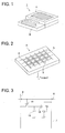
- Fig. 1 is a schematic drawing to show an example of a display device constituted of an organic EL element. It is a schematic drawing of a display, which displays image information by emission of an organic EL element, such as a mobile phone.
- Display 1 is constituted of such as display section A having plural number of pixels and control section B which performs image scanning of display section A based on image information.
- Control section B which is electrically connected to display section A, sends a scanning signal and an image data signal to plural number of pixels based on image information from the outside and pixels of each scanning line successively emit depending on the image data signal by a scanning signal to perform image scanning, whereby image information is displayed on display section A.
- Fig. 2 is a schematic drawing of display section A.
- Display section A is provided with such as a wiring part, which contains plural scanning lines 5 and data lines 6, and plural pixels 3 on a substrate. Primary part materials of display section A will be explained in the following.
- Scanning lines 5 and plural data lines 6 in a wiring part each are comprised of a conductive material, and scanning lines 5 and data lines 6 are perpendicular in a grid form and are connected to pixels 3 at the right-angled crossing points (details are not shown in the drawling).
- Pixel 3 receives an image data from data line 6 when a scanning signal is applied from scanning line 5 and emits according to the received image data.
- Full-color display device is possible by appropriately arranging pixels having an emission color in a red region, pixels in a green region and pixels in a blue region, side by side on the same substrate.
- Fig. 3 is a schematic drawing of a pixel.
- a pixel is equipped with such as organic EL element 10, switching transistor 11, operating transistor 12 and capacitor 13. Red, green and blue emitting organic EL elements are utilized as organic EL element 10 for plural pixels, and full-color display device is possible by arranging these side by side on the same substrate.
- an image data signal is applied on the drain of switching transistor 11 via data line 6 from control section B. Then, when a scanning signal is applied on the gate of switching transistor 11 via scanning line 5 from control section B, operation of switching transistor is on to transmit the image data signal applied on the drain to the gates of capacitor 13 and operating transistor 12.
- Operating transistor 12 is on, simultaneously with capacitor 13 being charged depending on the potential of an image data signal, by transmission of an image data signal.
- the drain is connected to electric source line 7 and the source is connected to the electrode of organic EL element 10, and an electric current is supplied from electric source line 7 to organic EL element 10 depending on the potential of an image data applied on the gate.
- emission of each organic EL element 10 of plural pixels 3 is performed by providing switching transistor 11 and operating transistor 12 against each organic EL element 10 of plural pixels 3. Such an emission method is called as an active matrix mode.
- emission of organic EL element 10 may be either emission of plural gradations based on a multiple-valued image data signal having plural number of gradation potentials or on and off of a predetermined emission quantity based on a binary image data signal. Further, potential hold of capacitor 13 may be either continuously maintained until the next scanning signal application or discharged immediately before the next scanning signal application.
- emission operation is not necessarily limited to the above-described active matrix mode but may be a passive matrix mode in which organic EL element is emitted based on a data signal only when a scanning signal is scanned.
- Fig. 4 is a schematic drawing of a display device based on a passive matrix mode.
- plural number of scanning lines 5 and plural number of image data lines 6 are arranged grid-wise, opposing to each other and sandwiching pixels 3.
- pixel 3 connected to scanning line 5 applied with said signal emits depending on an image data signal.
- pixel 3 is provided with no active element in a passive matrix mode, decrease of manufacturing cost is possible.
- An organic EL element material of this invention can be also applied to an organic EL element to generate emission of practically white color as an illumination device.
- Plural emission colors are simultaneously emitted by plural number of emission materials to obtain white light by mixing colors.
- a combination of plural emission colors may be either the one, in which three emission maximum wavelengths of three primary colors of blue, green and red are contained, or the other, in which two emission maximum wavelengths, utilizing a relationship of complimentary colors such as blue and yellow, or blue and orange, are contained.
- a combination of emission materials to obtain plural number of emission colors may be either a combination comprising plural number of materials which emit phosphoresce or fluorescence, or a combination of a material which emits phosphoresce or fluorescence and a dye material which emits by light from an emission material as exiting light, however, in a white organic electroluminescent element according to this invention, it is enough only to mix plural emission dopants in combination.
- a mask is provided only at the time of forming such as an emission layer, a positive hole transport layer or an electron transport layer, to only simply arrange the plural emission dopants such as by separately painting through the mask, while other layers are commonly utilized to require no patterning such as a mask.
- an electrode can be formed all over the plane by such as an evaporation method, a cast method, a spin coat method, an inkjet method and a printing method, resulting in improvement of productivity.
- an element itself is white emitting.
- An emission material utilized in an emission layer is not specifically limited, and in the case of a backlight of a liquid crystal display element, any combination by arbitrary selection among platinum complexes according to this invention or emission materials well known in the art can be utilized so as to be fitted to the wavelength range corresponding to CF (color filter) characteristics, whereby white emission can be obtained.
- a white emitting organic EL element of this invention is usefully utilized as one type of a lamp such as a home use illumination, a car room illumination or an exposure light source as various emission light sources or illumination devices, in addition to the aforesaid display device and a display, and is further usefully applied for a display as such as a backlight of a liquid crystal display.
- the transparent support substrate was washed with isopropyl alcohol by use of ultrasonic waves, followed by being dried with a dry nitrogen gas, and was subjected to UV ozone washing for 5 minutes.
- This transparent support substrate was fixed on a substrate holder of a vacuum evaporation system available on the market, and on the other hand, each of five resistance heating boats made of tantalum was charged with ⁇ -NPD, H4, Ir-12, BCP and Alq 3 , respectively, which was attached in the vacuum evaporation system (in the first vacuum chamber).
- a resistance heating boat made of tantalum was charged with lithium fluoride and a resistance heating boat made of tungsten was charged with aluminum, respectively, and these boats were attached in the second chamber of the vacuum evaporation system.
- the aforesaid heating boat charged with ⁇ -NPD was heated with an electric current to deposit ⁇ -NPD on a support substrate at a deposition rate of 0.1 - 0.2 nm/sec so as to make a layer thickness of 20 nm, whereby a positive hole injection/transport layer was formed.
- the aforesaid heating boat charged with H4 and the boat charged with Ir-12 were independently supplied with an electric current to deposit H4 as an emission host and Ir-12 as an emission dopant so as to make a layer thickness of 30 nm while adjusting the deposition rates thereof to 100 : 6, whereby an emission layer was formed.
- the aforesaid heating boat charged with BCP was heated with an electric current to provide a positive hole inhibition layer having a layer thickness of 10 nm at a deposition rate of 0.1 - 0.2 nm/sec. Further, the aforesaid heating boat charged with Alq 3 was heated with an electric current to provide an electron transport layer having a layer thickness of 20 nm at a deposition rate of 0.1 - 0.2 nm/sec.
- a mask which was made of stainless steel and had rectangular holes, was arranged on the electron injection layer by means of remote control from outside of the system.
- a boat charged with lithium fluoride was supplied with an electric current to provide a cathode buffer layer having a layer thickness of 0.5 nm at a deposition rate of 0.01 - 0.02 nm/sec, and then a boat charged with aluminum was supplied with an electric current to provide a cathode having a layer thickness of 150 nm at a deposition rate of 1 - 2 nm/sec to obtain Organic EL Element 1-1.
- Organic EL elements 1-2 - 1-21 each were prepared in a similar manner to preparation of organic EL element 1-1 described above, except that an emission dopant was changed as shown in table 2.
- Fig. 5 is a schematic view of a lighting device.
- Organic EL element 101 is covered with glass cover 102 (sealing operation employing the glass cover was carried out in a globe box (under an atmosphere of high purity nitrogen gas at a purity of at least 99.999%) without contact with atmospheric air).
- Fig. 6 is a sectional view of the lighting device, in which numeral 105 represents a cathode, 106 represents an organic EL layer, and 107 represents a glass substrate fitted with a transparent electrode. Further, nitrogen gas 108 is fed into glass cover 102, and desiccant 109 is provided.
- Each of organic EL elements was lighted under a constant current condition of 2.5 mA/cm 2 at room temperature (approximately 23 - 25 °C), and an emission luminance (L) [cd/m 2 ] immediately after turning on was measured, whereby a quantum efficiency of taking out ( ⁇ ) was calculated.
- CS-1000 produced by Konica Minolta Sensing Inc.
- each of the quantum efficiency of taking out was expressed as a relative value when that of organic EL element 1-1 was set to 100.
- Each of organic EL elements was continuously lighted under a constant current condition of 2.5 mA/cm 2 at room temperature (approximately 23 - 25°C), and time to reach a half of the initial luminance ( ⁇ 1/2) was measured. Further, each emission life was expressed as a relative value when that of organic EL element 1-1 was set to 100.
- Each of organic EL elements was continuously lighted under a constant current condition of 2.5 mA/cm 2 at room temperature. The luminescent color was visibly observed and evaluated.
- the organic EL elements prepared via the metal complexes according to the present invention attain high luminescent efficiency and extended luminescent lifetime, compared to the EL element of the Comparative Examples.
- the purity of blue color is higher, resulting in a more useful blue luminescent element.
- a derivative having the ring structure in which at least one carbon atom of the hydrocarbon ring constituting the carboline derivative or the carboline ring of the carboline derivative was substituted with a nitrogen atom targeted effects of the present invention were further enhanced.
- the transparent support substrate was washed with isopropyl alcohol by use of ultrasonic waves, followed by being dried with a dry nitrogen gas, and was subjected to UV ozone washing for 5 minutes.
- This transparent support substrate was fixed on a substrate holder of a vacuum evaporation system available on the market, and on the other hand, each of five resistance heating boats made of tantalum was charged with ⁇ -NPD, H2, Ir-13, BCP and Alq 3 , respectively, which was attached in the vacuum evaporation system (in the first vacuum chamber).
- a resistance heating boat made of tantalum was charged with lithium fluoride and a resistance heating boat made of tungsten was charged with aluminum, respectively, and these boats were attached in the second chamber of the vacuum evaporation system.
- the aforesaid heating boat charged with ⁇ -NPD was heated with an electric current to deposit ⁇ -NPD on a support substrate at a deposition rate of 0.1 - 0.2 nm/sec so as to make a layer thickness of 20 nm, whereby a positive hole injection/transport layer was formed.
- the aforesaid heating boat charged with H2 and the boat charged with Ir-13 were independently supplied with an electric current to deposit H2 as an emission host and Ir-13 as an emission dopant so as to make a layer thickness of 30 nm while adjusting the deposition rates thereof to 100 : 6, whereby an emission layer was formed.
- the aforesaid heating boat charged with BCP was heated with an electric current to provide a positive hole inhibition layer having a layer thickness of 10 nm at a deposition rate of 0.1 - 0.2 nm/sec. Further, the aforesaid heating boat charged with Alq 3 was heated with an electric current to provide an electron transport layer having a layer thickness of 20 nm at a deposition rate of 0.1 - 0.2 nm/sec.
- a mask which was made of stainless steel and had rectangular holes, was arranged on the electron injection layer by means of remote control from outside of the system.
- Organic EL elements 2-2 -2-31 each were prepared in a similar manner to preparation of organic EL element 2-1 described above, except that an emission dopant was changed as shown in table 3.
- BCP 94 100 bluish green Comp. 2-7 H2 Comparative 8 BCP 108 94 yellow Comp. 2-8 H2 Comparative 9 BCP 125 889 yellow Comp. 2-9 H2 (7) BCP 135 360 pure blue Inv. 2-10 H2 (27) BCP 140 372 pure blue Inv. 2-11 H2 (38) BCP 142 368 pure blue Inv. 2-12 H4 (56) BCP 151 582 blue Inv. 2-13 H4 (77) BCP 153 603 blue Inv. 2-14 H4 (97) BCP 156 707 bluish green Inv. 2-15 H4 (106) BCP 149 668 blue Inv. 2-16 H6 (113) BCP 154 692 blue Inv.
- BCP 148 671 blue Inv. 2-18 H6 (139) BCP 159 721 blue Inv. 2-19 H6 (144) BCP 157 764 pure blue Inv. 2-20 H10 (148) BCP 155 738 pure blue Inv. 2-21 H10 (152) BCP 158 756 blue Inv. 2-22 H10 (157) BCP 156 744 pure blue Inv. 2-23 H10 (159) BCP 152 715 pure blue Inv. 2-24 H2 (7) H5 141 399 pure blue Inv. 2-25 H4 (56) H5 156 615 blue Inv. 2-26 H4 (97) H5 161 738 bluish green Inv. 2-27 H6 (119) H5 154 698 Blue Inv.
- the surface resistance of the resulting cathode was 10 ⁇ / ⁇ .
- polyvinylcarbazole being a positive hole transporting binder polymer
- Ir-13 being a blue fluorescent ortho metal complex
- 2-(4-biphenylyl-5(4-t-butylphenyl)-1,3,4-oxazole being an electron transport material
- a mask (being a mask resulting in a luminescent area of 5 mm x 5 mm), which was subjected to patterning, was arranged and an anode was arranged in such a manner that in a vacuum evaporation device, 0.5 mm lithium fluoride was evaporated as an anode buffer layer and 150 nm aluminum as a cathode was evaporated, whereby Blue Luminescent Organic EL Element 3-1 was prepared.
- Organic EL Elements 3-2 - 3-11 were prepared in the same manner as Organic EL Element 3-1, except that the emission dopant was changed as described in Table 4.
- Organic EL element 1-18 of example 1 was utilized as a blue emission element.
- a green emission element was prepared by substituting Ir-13 used in Organic EL element 2-1 of Example 2 with Ir-1.
- a red emission element was prepared by substituting Ir-13 used in Organic EL element 2-1 of Example 2 with Ir-9.
- Each of red, green and blue organic EL elements prepared above was arranged parallel on the same substrate to prepare an active matrix mode full-color having a form as described in Fig. 1 , and only display section A of said display device is schematically shown in Fig. 2 .
- a wiring section containing plural lines of scanning line 5 and data line 6, and plural pixels 3 (such as a pixel having an emission color of a red region, a pixel of a green region and a pixel of a blue region) arranged parallel are provided on the same substrate, and scanning lines 5 and data lines 6 in a wiring section, which are comprised of a conductive material, respectively, cross each other at a right angle in a grid form to be connected to pixels 3 at the right-angled crossing points (details being not shown in the drawing).
- the aforesaid plural pixels 3 each are operated in an active matrix mode, in which an organic EL element, a switching transistor and an operating transistor are provided corresponding to each emission color, and receive an image data signal from data line 6 when a scanning signal is applied from scanning line 5 to emit based on the received image data.
- Each red, green and blue pixel was appropriately arranged parallel in this manner, whereby a full-color display device was prepared.
- a transparent electrode substrate of example 1 was subjected to patterning of an electrode having an area of 20 mm x 20 mm, and ⁇ -NPD was deposited thereon at a layer thickness of 25 nm as a positive hole injection/transport layer in a similar manner to example 1; and further the aforesaid heating boat charged with H4, boat containing Example compound (159) and boat containing Ir-9 were supplied with an electric current to deposit an emission layer having a layer thickness of 30 nm, while adjusting the evaporation rates of CBP as an emission host, Example compound (159) and Ir-9 as emission dopants to be 100 : 5 : 0.6.
- BCP was deposited at 10 nm to provide a positive hole inhibition layer.
- Alq 3 was deposited at 40 nm to provide an electron transport layer.
- a mask with square holes having a shape nearly same as a transparent electrode made of stainless steel was arranged on an electron injection layer, and 0.5 nm of lithium fluoride as a cathode buffer layer and 150 nm of aluminum as a cathode were deposited.
- This element was equipped with a sealed can, which had a similar structure and was prepared in a similar method to example 1, to prepare flat lamps shown in Figs. 5 and 6 .
- the resulting transparent substrate fitted with the above ITO transparent electrode was subjected to ultrasonic washing employing isopropyl alcohol and dried via desiccated nitrogen gas, and then subjected to UV ozone cleaning for 5 minutes.
- a solution prepared by diluting poly(3,4-ethylenedioxythiophene)-polystyrenesulfonate (PEDOT/PSS, produced by Bayer Co., BASYTRON P A1 4083) with pure water to 70% by weight was applied to the resulting transparent substrate at 3,000 rpm over 30 seconds, employing a spin coating method, and subsequently dried at 200 °C over 1 hour, whereby a 30 nm thick positive hole injection transport layer was resulted.
- PEDOT/PSS poly(3,4-ethylenedioxythiophene)-polystyrenesulfonate
- a solution prepared by dissolving 30 mg of exemplified compound 186 of the present invention in 3 ml of toluene was applied onto the resulting positive hole injection transport layer at 1,000 rpm over 30 seconds, employing a spin coating method, and subsequently dried for one hour under vacuum, whereby a 80 mm thick emission layer was prepared.
- Each of Organic EL Elements 6-2 - 6-17 was prepared in the same manner as Organic Element 6-1, except that exemplified compound 186 employed to prepare the luminance layer was replaced with each of 187, 188, 192, 193, 195, 196, 198, 200, 202, 204, 205, 207, 209, 210, 214, and 215.
- exemplified compound 186 employed to prepare the luminance layer was replaced with each of 187, 188, 192, 193, 195, 196, 198, 200, 202, 204, 205, 207, 209, 210, 214, and 215.
- Organic EL Element 6-18 was prepared in the same manner as Organic EL Element 6-1, except that 3 ml of the solution of exemplified compound 186 of the present invention was replaced with the solution described in following (A).
- Determination was carried out also employing a spectral radiance meter CS-1000 (produced by Konica Minolta Holdings, Inc.).
- Measurement results of the taking-out quantum efficiency and the luminescent lifetime of Organic EL Elements 6-1 - 6-18 were subjected to relative evaluation when each value of Organic EL Element 6-18 was to be 100.
- Table 5 shows the results.
- Table 5 Organic EL Element No. Material in emission Layer Taking-out Quantum Yield (relative value)
- Luminescent Lifetime Luminescent Color Remarks 6-1 186 139 529 blue Inv. 6-2 187 148 685 blue Inv. 6-3 188 152 531 blue Inv. 6-4 192 160 458 blue Inv. 6-5 193 141 624 blue Inv. 6-6 195 155 652 blue Inv. 6-7 196 121 418 blue Inv. 6-8 198 172 713 blue Inv. 6-9 200 154 851 blue Inv. 6-10 202 132 366 blue Inv. 6-11 204 115 584 blue Inv. 6-12 205 128 759 blue Inv.
- Element (6-16) employing PO-29 of the present invention resulted in green luminescence
- Element (6-17) employing PO-30 of the present invention resulted in red luminescence
- Organic EL Elements other than those resulted in blue luminescence.
Landscapes
- Chemical & Material Sciences (AREA)
- Engineering & Computer Science (AREA)
- Materials Engineering (AREA)
- Organic Chemistry (AREA)
- Crystallography & Structural Chemistry (AREA)
- Inorganic Chemistry (AREA)
- Electroluminescent Light Sources (AREA)
Applications Claiming Priority (2)
| Application Number | Priority Date | Filing Date | Title |
|---|---|---|---|
| JP2006042061 | 2006-02-20 | ||
| PCT/JP2007/051157 WO2007097153A1 (fr) | 2006-02-20 | 2007-01-25 | Substance d'élément électroluminescent organique, élément électroluminescent organique, dispositif d'affichage et dispositif d'éclairage |
Publications (2)
| Publication Number | Publication Date |
|---|---|
| EP1988144A1 true EP1988144A1 (fr) | 2008-11-05 |
| EP1988144A4 EP1988144A4 (fr) | 2010-07-21 |
Family
ID=38428599
Family Applications (2)
| Application Number | Title | Priority Date | Filing Date |
|---|---|---|---|
| EP07707233A Ceased EP1988143A4 (fr) | 2006-02-20 | 2007-01-23 | Élément électroluminescent organique, élément émettant une lumière blanche, dispositif d'affichage et dispositif d'éclairage |
| EP07707404A Withdrawn EP1988144A4 (fr) | 2006-02-20 | 2007-01-25 | Substance d'élément électroluminescent organique, élément électroluminescent organique, dispositif d'affichage et dispositif d'éclairage |
Family Applications Before (1)
| Application Number | Title | Priority Date | Filing Date |
|---|---|---|---|
| EP07707233A Ceased EP1988143A4 (fr) | 2006-02-20 | 2007-01-23 | Élément électroluminescent organique, élément émettant une lumière blanche, dispositif d'affichage et dispositif d'éclairage |
Country Status (4)
| Country | Link |
|---|---|
| US (2) | US20070196690A1 (fr) |
| EP (2) | EP1988143A4 (fr) |
| JP (4) | JP5520479B2 (fr) |
| WO (2) | WO2007097149A1 (fr) |
Cited By (2)
| Publication number | Priority date | Publication date | Assignee | Title |
|---|---|---|---|---|
| US9005773B2 (en) | 2010-03-15 | 2015-04-14 | Semiconductor Energy Laboratory Co., Ltd. | Organometallic complex, light-emitting element, display device, electronic device, and lighting device |
| DE202015009141U1 (de) | 2015-10-15 | 2016-11-03 | Tesa Se | Klebemasse, insbesondere für stripbare Klebestreifen, und Verwendung zur Verklebung auf getrichener Raufasertapete |
Families Citing this family (81)
| Publication number | Priority date | Publication date | Assignee | Title |
|---|---|---|---|---|
| JP5520479B2 (ja) | 2006-02-20 | 2014-06-11 | コニカミノルタ株式会社 | 有機エレクトロルミネッセンス素子、白色発光素子、及び照明装置 |
| JP5181448B2 (ja) * | 2006-09-13 | 2013-04-10 | コニカミノルタホールディングス株式会社 | 有機エレクトロルミネッセンス素子材料 |
| WO2008035571A1 (fr) * | 2006-09-20 | 2008-03-27 | Konica Minolta Holdings, Inc. | Élément électroluminescent organique |
| JP5577701B2 (ja) * | 2007-07-12 | 2014-08-27 | コニカミノルタ株式会社 | 有機エレクトロルミネッセンス素子材料、有機エレクトロルミネッセンス素子、表示装置及び照明装置 |
| CN102119205A (zh) * | 2008-06-10 | 2011-07-06 | 巴斯夫欧洲公司 | 新型过渡金属配合物及其在有机发光二极管-iv中的用途 |
| US8410270B2 (en) | 2008-06-10 | 2013-04-02 | Basf Se | Transition metal complexes and use thereof in organic light-emitting diodes V |
| KR101656793B1 (ko) * | 2008-06-10 | 2016-09-12 | 유디씨 아일랜드 리미티드 | 신규한 전이 금속 착물 및 이의 유기 발광 다이오드에서의 용도 - ⅲ |
| US8859110B2 (en) * | 2008-06-20 | 2014-10-14 | Basf Se | Cyclic phosphazene compounds and use thereof in organic light emitting diodes |
| JP5609641B2 (ja) * | 2008-07-10 | 2014-10-22 | コニカミノルタ株式会社 | 有機エレクトロルミネッセンス素子、表示装置及び照明装置 |
| US8815415B2 (en) * | 2008-12-12 | 2014-08-26 | Universal Display Corporation | Blue emitter with high efficiency based on imidazo[1,2-f] phenanthridine iridium complexes |
| WO2011052250A1 (fr) * | 2009-10-26 | 2011-05-05 | コニカミノルタホールディングス株式会社 | Élément électroluminescent organique, matériau pour éléments électroluminescents organiques, dispositif d'affichage et dispositif d'éclairage |
| KR101288574B1 (ko) * | 2009-12-02 | 2013-07-22 | 제일모직주식회사 | 갭필용 충전제 및 상기 충전제를 사용한 반도체 캐패시터의 제조 방법 |
| US9156870B2 (en) * | 2010-02-25 | 2015-10-13 | Universal Display Corporation | Phosphorescent emitters |
| JP5507381B2 (ja) | 2010-07-30 | 2014-05-28 | ユー・ディー・シー アイルランド リミテッド | 有機電界発光素子及び化合物 |
| US20130285035A1 (en) * | 2011-01-12 | 2013-10-31 | Konica Minolta, Inc. | Organic electroluminescent element, lighting device, and display device |
| KR102120606B1 (ko) * | 2011-02-23 | 2020-06-09 | 유니버셜 디스플레이 코포레이션 | 신규한 4좌 백금 착물 |
| WO2012162488A1 (fr) | 2011-05-26 | 2012-11-29 | Arizona Board Of Regents Acting For And On Behalf Of Arizona State University | Synthèse de complexes de platine et de palladium comme émetteurs phosphorescents à bande étroite pour dispositifs d'affichage pleine couleur |
| JP5938756B2 (ja) * | 2011-06-15 | 2016-06-22 | コニカミノルタ株式会社 | 有機エレクトロルミネッセンス素子および照明装置 |
| US10211413B2 (en) * | 2012-01-17 | 2019-02-19 | Universal Display Corporation | Organic electroluminescent materials and devices |
| JP5978843B2 (ja) | 2012-02-02 | 2016-08-24 | コニカミノルタ株式会社 | イリジウム錯体化合物、有機エレクトロルミネッセンス素子材料、有機エレクトロルミネッセンス素子、照明装置及び表示装置 |
| JP5765271B2 (ja) * | 2012-03-02 | 2015-08-19 | コニカミノルタ株式会社 | 有機エレクトロルミネッセンス素子、表示装置および照明装置 |
| EP2882763B1 (fr) | 2012-08-07 | 2018-08-22 | Merck Patent GmbH | Complexes métalliques |
| US9978958B2 (en) * | 2012-08-24 | 2018-05-22 | Universal Display Corporation | Phosphorescent emitters with phenylimidazole ligands |
| JP6119754B2 (ja) * | 2012-09-04 | 2017-04-26 | コニカミノルタ株式会社 | 有機エレクトロルミネッセンス素子、照明装置及び表示装置 |
| US9882150B2 (en) | 2012-09-24 | 2018-01-30 | Arizona Board Of Regents For And On Behalf Of Arizona State University | Metal compounds, methods, and uses thereof |
| WO2014109814A2 (fr) | 2012-10-26 | 2014-07-17 | Arizona Board Of Regents Acting For And On Behalf Of Arizona State University | Complexes métalliques, procédés, et utilisations de ces derniers |
| US8946697B1 (en) * | 2012-11-09 | 2015-02-03 | Universal Display Corporation | Iridium complexes with aza-benzo fused ligands |
| US9685617B2 (en) | 2012-11-09 | 2017-06-20 | Universal Display Corporation | Organic electronuminescent materials and devices |
| US9748500B2 (en) | 2015-01-15 | 2017-08-29 | Universal Display Corporation | Organic light emitting materials |
| US9634264B2 (en) | 2012-11-09 | 2017-04-25 | Universal Display Corporation | Organic electroluminescent materials and devices |
| JP5472430B2 (ja) * | 2012-11-20 | 2014-04-16 | コニカミノルタ株式会社 | 有機エレクトロルミネッセンス素子材料 |
| JP5630511B2 (ja) * | 2013-02-06 | 2014-11-26 | コニカミノルタ株式会社 | 有機エレクトロルミネッセンス素子材料、有機エレクトロルミネッセンス素子、表示装置及び照明装置 |
| JP5626384B2 (ja) * | 2013-02-06 | 2014-11-19 | コニカミノルタ株式会社 | 有機エレクトロルミネッセンス素子材料、有機エレクトロルミネッセンス素子、表示装置及び照明装置 |
| JP6085985B2 (ja) * | 2013-02-12 | 2017-03-01 | コニカミノルタ株式会社 | 有機金属錯体、有機エレクトロルミネッセンス素子材料、有機エレクトロルミネッセンス素子、照明装置及び表示装置 |
| KR102049684B1 (ko) * | 2013-03-29 | 2019-11-28 | 코니카 미놀타 가부시키가이샤 | 이성체 혼합 금속 착체 조성물, 유기 일렉트로루미네센스 소자, 조명 장치 및 표시 장치 |
| JP5556929B2 (ja) * | 2013-05-01 | 2014-07-23 | コニカミノルタ株式会社 | 有機エレクトロルミネッセンス素子材料 |
| CN104232076B (zh) | 2013-06-10 | 2019-01-15 | 代表亚利桑那大学的亚利桑那校董会 | 具有改进的发射光谱的磷光四齿金属络合物 |
| US9929359B2 (en) | 2013-07-17 | 2018-03-27 | Sumitomo Chemical Company, Limited | Composition and light emitting device using the same |
| JP6804823B2 (ja) | 2013-10-14 | 2020-12-23 | アリゾナ・ボード・オブ・リージェンツ・オン・ビハーフ・オブ・アリゾナ・ステイト・ユニバーシティーArizona Board of Regents on behalf of Arizona State University | 白金錯体およびデバイス |
| US10797248B2 (en) * | 2013-12-09 | 2020-10-06 | Konica Minolta, Inc. | Organic electroluminescent element, lighting device, and display device |
| US10020455B2 (en) | 2014-01-07 | 2018-07-10 | Arizona Board Of Regents On Behalf Of Arizona State University | Tetradentate platinum and palladium complex emitters containing phenyl-pyrazole and its analogues |
| US11005050B2 (en) | 2014-01-13 | 2021-05-11 | Merck Patent Gmbh | Metal complexes |
| KR20150127494A (ko) * | 2014-05-07 | 2015-11-17 | 삼성전자주식회사 | 유기금속 화합물 및 이를 포함한 유기 발광 소자 |
| US9941479B2 (en) | 2014-06-02 | 2018-04-10 | Arizona Board Of Regents On Behalf Of Arizona State University | Tetradentate cyclometalated platinum complexes containing 9,10-dihydroacridine and its analogues |
| US9923155B2 (en) | 2014-07-24 | 2018-03-20 | Arizona Board Of Regents On Behalf Of Arizona State University | Tetradentate platinum (II) complexes cyclometalated with functionalized phenyl carbene ligands and their analogues |
| WO2016025921A1 (fr) | 2014-08-15 | 2016-02-18 | Arizona Board Of Regents On Behalf Of Arizona State University | Complexes de métal non platine pour diodes électroluminescentes organiques blanches à dopant unique à base d'excimère |
| US11329244B2 (en) | 2014-08-22 | 2022-05-10 | Arizona Board Of Regents On Behalf Of Arizona State University | Organic light-emitting diodes with fluorescent and phosphorescent emitters |
| US9920242B2 (en) | 2014-08-22 | 2018-03-20 | Arizona Board Of Regents On Behalf Of Arizona State University | Metal-assisted delayed fluorescent materials as co-host materials for fluorescent OLEDs |
| US9865825B2 (en) | 2014-11-10 | 2018-01-09 | Arizona Board Of Regents On Behalf Of Arizona State University | Emitters based on octahedral metal complexes |
| US10033003B2 (en) | 2014-11-10 | 2018-07-24 | Arizona Board Of Regents On Behalf Of Arizona State University | Tetradentate metal complexes with carbon group bridging ligands |
| JP6534853B2 (ja) * | 2015-04-21 | 2019-06-26 | 三星ディスプレイ株式會社Samsung Display Co.,Ltd. | 有機エレクトロルミネッセンス素子用材料及びそれを用いた有機エレクトロルミネッセンス素子およびその製造方法 |
| US9879039B2 (en) | 2015-06-03 | 2018-01-30 | Arizona Board Of Regents On Behalf Of Arizona State University | Tetradentate and octahedral metal complexes containing naphthyridinocarbazole and its analogues |
| WO2016197019A1 (fr) | 2015-06-04 | 2016-12-08 | Jian Li | Dispositifs électroluminescents transparents à écrans émissifs unilatéraux commandés |
| KR102486382B1 (ko) * | 2015-08-03 | 2023-01-09 | 삼성전자주식회사 | 유기금속 화합물 및 이를 포함한 유기 발광 소자 |
| JP6044695B2 (ja) * | 2015-11-16 | 2016-12-14 | コニカミノルタ株式会社 | 有機エレクトロルミネッセンス素子、それが具備された表示装置及び照明装置 |
| KR20220000988A (ko) | 2016-01-29 | 2022-01-04 | 스미또모 가가꾸 가부시키가이샤 | 조성물, 인광 발광성 화합물 및 발광 소자 |
| KR20170108845A (ko) * | 2016-03-18 | 2017-09-27 | 가부시키가이샤 한도오따이 에네루기 켄큐쇼 | 유기 금속 착체, 발광 소자, 발광 장치, 전자 기기 및 조명 장치 |
| US11335865B2 (en) | 2016-04-15 | 2022-05-17 | Arizona Board Of Regents On Behalf Of Arizona State University | OLED with multi-emissive material layer |
| US20170324049A1 (en) * | 2016-05-05 | 2017-11-09 | Universal Display Corporation | Organic Electroluminescent Materials and Devices |
| GB2550203A (en) * | 2016-05-13 | 2017-11-15 | Sumitomo Chemical Co | Light-emitting compound |
| US10177323B2 (en) | 2016-08-22 | 2019-01-08 | Arizona Board Of Regents On Behalf Of Arizona State University | Tetradentate platinum (II) and palladium (II) complexes and octahedral iridium complexes employing azepine functional groups and their analogues |
| KR102888327B1 (ko) | 2016-10-12 | 2025-11-18 | 아리조나 보드 오브 리젠츠 온 비하프 오브 아리조나 스테이트 유니버시티 | 협대역 적색 인광성 4좌 백금(ii) 착물 |
| US11545636B2 (en) * | 2016-12-15 | 2023-01-03 | Universal Display Corporation | Organic electroluminescent materials and devices |
| US11183670B2 (en) | 2016-12-16 | 2021-11-23 | Arizona Board Of Regents On Behalf Of Arizona State University | Organic light emitting diode with split emissive layer |
| WO2018140765A1 (fr) | 2017-01-27 | 2018-08-02 | Jian Li | Émetteurs fluorescents retardés assistés par un métal utilisant des pyrido-pyrrolo-acridine et des analogues |
| US20200411773A1 (en) | 2017-04-27 | 2020-12-31 | Sumitomo Chemical Company, Limited | Composition and light emitting device using the same |
| WO2018198972A1 (fr) | 2017-04-27 | 2018-11-01 | 住友化学株式会社 | Composition et élément électroluminescent la comprenant |
| KR102527229B1 (ko) * | 2017-05-10 | 2023-05-02 | 삼성디스플레이 주식회사 | 유기금속 화합물 및 이를 포함한 유기 발광 소자 |
| US10516117B2 (en) | 2017-05-19 | 2019-12-24 | Arizona Board Of Regents On Behalf Of Arizona State University | Metal-assisted delayed fluorescent emttters employing benzo-imidazo-phenanthridine and analogues |
| US11101435B2 (en) | 2017-05-19 | 2021-08-24 | Arizona Board Of Regents On Behalf Of Arizona State University | Tetradentate platinum and palladium complexes based on biscarbazole and analogues |
| US11647643B2 (en) | 2017-10-17 | 2023-05-09 | Arizona Board Of Regents On Behalf Of Arizona State University | Hole-blocking materials for organic light emitting diodes |
| WO2019079508A2 (fr) | 2017-10-17 | 2019-04-25 | Jian Li | Excimères phosphorescents à orientation moléculaire préférée en tant qu'émetteurs monochromatiques destinés à des applications d'affichage et d'éclairage |
| US12075690B2 (en) * | 2017-12-14 | 2024-08-27 | Universal Display Corporation | Organic electroluminescent materials and devices |
| US12037348B2 (en) | 2018-03-09 | 2024-07-16 | Arizona Board Of Regents On Behalf Of Arizona State University | Blue and narrow band green and red emitting metal complexes |
| US11878988B2 (en) | 2019-01-24 | 2024-01-23 | Arizona Board Of Regents On Behalf Of Arizona State University | Blue phosphorescent emitters employing functionalized imidazophenthridine and analogues |
| US11594691B2 (en) | 2019-01-25 | 2023-02-28 | Arizona Board Of Regents On Behalf Of Arizona State University | Light outcoupling efficiency of phosphorescent OLEDs by mixing horizontally aligned fluorescent emitters |
| US11785838B2 (en) | 2019-10-02 | 2023-10-10 | Arizona Board Of Regents On Behalf Of Arizona State University | Green and red organic light-emitting diodes employing excimer emitters |
| JP7216754B2 (ja) | 2020-03-31 | 2023-02-01 | 住友化学株式会社 | 組成物及びそれを含有する発光素子 |
| CN113683625B (zh) | 2020-05-19 | 2025-06-10 | 亚利桑那州立大学董事会 | 用于有机发光二极管的金属辅助延迟荧光发射体 |
| US11945985B2 (en) | 2020-05-19 | 2024-04-02 | Arizona Board Of Regents On Behalf Of Arizona State University | Metal assisted delayed fluorescent emitters for organic light-emitting diodes |
| KR102896743B1 (ko) * | 2021-01-18 | 2025-12-05 | 삼성디스플레이 주식회사 | 유기금속 화합물 및 이를 응용한 발광 소자 |
Family Cites Families (123)
| Publication number | Priority date | Publication date | Assignee | Title |
|---|---|---|---|---|
| JP2814435B2 (ja) | 1987-03-02 | 1998-10-22 | イーストマン・コダック・カンパニー | 改良薄膜発光帯をもつ電場発光デバイス |
| JP2815472B2 (ja) | 1990-01-22 | 1998-10-27 | パイオニア株式会社 | 電界発光素子 |
| US5061569A (en) | 1990-07-26 | 1991-10-29 | Eastman Kodak Company | Electroluminescent device with organic electroluminescent medium |
| JP3016896B2 (ja) | 1991-04-08 | 2000-03-06 | パイオニア株式会社 | 有機エレクトロルミネッセンス素子 |
| US5294870A (en) * | 1991-12-30 | 1994-03-15 | Eastman Kodak Company | Organic electroluminescent multicolor image display device |
| EP0610514B1 (fr) | 1992-08-28 | 2003-04-02 | Idemitsu Kosan Company Limited | Aide d'injection de charge et dispositif electroluminescent organique le contenant |
| JPH06325871A (ja) | 1993-05-18 | 1994-11-25 | Mitsubishi Kasei Corp | 有機電界発光素子 |
| US5707745A (en) * | 1994-12-13 | 1998-01-13 | The Trustees Of Princeton University | Multicolor organic light emitting devices |
| JP3561549B2 (ja) | 1995-04-07 | 2004-09-02 | 三洋電機株式会社 | 有機エレクトロルミネッセンス素子 |
| JP3529543B2 (ja) | 1995-04-27 | 2004-05-24 | パイオニア株式会社 | 有機エレクトロルミネッセンス素子 |
| US5719467A (en) | 1995-07-27 | 1998-02-17 | Hewlett-Packard Company | Organic electroluminescent device |
| JP3645642B2 (ja) | 1996-03-25 | 2005-05-11 | Tdk株式会社 | 有機エレクトロルミネセンス素子 |
| US5776622A (en) | 1996-07-29 | 1998-07-07 | Eastman Kodak Company | Bilayer eletron-injeting electrode for use in an electroluminescent device |
| JP3852509B2 (ja) | 1998-01-09 | 2006-11-29 | ソニー株式会社 | 電界発光素子及びその製造方法 |
| JPH11204359A (ja) | 1998-01-14 | 1999-07-30 | Tokin Corp | 圧粉磁芯の製造方法と製造装置 |
| US6097147A (en) | 1998-09-14 | 2000-08-01 | The Trustees Of Princeton University | Structure for high efficiency electroluminescent device |
| GB9820805D0 (en) | 1998-09-25 | 1998-11-18 | Isis Innovation | Divalent lanthanide metal complexes |
| BRPI0009215B1 (pt) | 1999-03-23 | 2017-05-09 | Univ Southern California | complexos metálicos ciclometalizados como dopantes fosforescentes em diodos emissores de luz orgânicos |
| EP1729327B2 (fr) | 1999-05-13 | 2022-08-10 | The Trustees Of Princeton University | Utilisation d'un composé d'iridium phosphorescent comme molécule émissive dans un dispositif électroluminescent organique |
| US6461747B1 (en) * | 1999-07-22 | 2002-10-08 | Fuji Photo Co., Ltd. | Heterocyclic compounds, materials for light emitting devices and light emitting devices using the same |
| JP2001181617A (ja) | 1999-12-27 | 2001-07-03 | Fuji Photo Film Co Ltd | オルトメタル化白金錯体からなる発光素子材料および発光素子 |
| JP2001181616A (ja) | 1999-12-27 | 2001-07-03 | Fuji Photo Film Co Ltd | オルトメタル化パラジウム錯体からなる発光素子材料および発光素子 |
| JP3929689B2 (ja) | 2000-03-28 | 2007-06-13 | 富士フイルム株式会社 | 高効率赤色発光素子、イリジウム錯体から成る発光素子材料及び新規イリジウム錯体 |
| JP3929690B2 (ja) | 1999-12-27 | 2007-06-13 | 富士フイルム株式会社 | オルトメタル化イリジウム錯体からなる発光素子材料、発光素子および新規イリジウム錯体 |
| JP3929706B2 (ja) | 2000-02-10 | 2007-06-13 | 富士フイルム株式会社 | イリジウム錯体からなる発光素子材料及び発光素子 |
| JP4890669B2 (ja) | 2000-03-13 | 2012-03-07 | Tdk株式会社 | 有機el素子 |
| JP2002008860A (ja) | 2000-04-18 | 2002-01-11 | Mitsubishi Chemicals Corp | 有機電界発光素子 |
| JP2002015871A (ja) | 2000-04-27 | 2002-01-18 | Toray Ind Inc | 発光素子 |
| JP2001313178A (ja) | 2000-04-28 | 2001-11-09 | Pioneer Electronic Corp | 有機エレクトロルミネッセンス素子 |
| JP2001313179A (ja) | 2000-05-01 | 2001-11-09 | Mitsubishi Chemicals Corp | 有機電界発光素子 |
| JP4048521B2 (ja) | 2000-05-02 | 2008-02-20 | 富士フイルム株式会社 | 発光素子 |
| JP4382961B2 (ja) | 2000-05-02 | 2009-12-16 | 富士フイルム株式会社 | 発光素子 |
| JP4683766B2 (ja) | 2000-05-22 | 2011-05-18 | 株式会社半導体エネルギー研究所 | アクティブマトリクス型発光装置 |
| JP5062797B2 (ja) | 2000-05-22 | 2012-10-31 | 昭和電工株式会社 | 有機エレクトロルミネッセンス素子および発光材料 |
| US6645645B1 (en) | 2000-05-30 | 2003-11-11 | The Trustees Of Princeton University | Phosphorescent organic light emitting devices |
| JP2002062824A (ja) | 2000-06-05 | 2002-02-28 | Semiconductor Energy Lab Co Ltd | 発光装置 |
| US9697650B2 (en) | 2000-06-09 | 2017-07-04 | Flash Seats, Llc | Method and system for access verification within a venue |
| JP4290858B2 (ja) | 2000-06-12 | 2009-07-08 | 富士フイルム株式会社 | 有機電界発光素子 |
| JP2002083684A (ja) | 2000-06-23 | 2002-03-22 | Semiconductor Energy Lab Co Ltd | 発光装置 |
| JP4712232B2 (ja) | 2000-07-17 | 2011-06-29 | 富士フイルム株式会社 | 発光素子及びアゾール化合物 |
| JP4340401B2 (ja) | 2000-07-17 | 2009-10-07 | 富士フイルム株式会社 | 発光素子及びイリジウム錯体 |
| JP2002043056A (ja) | 2000-07-19 | 2002-02-08 | Canon Inc | 発光素子 |
| EP1325671B1 (fr) | 2000-08-11 | 2012-10-24 | The Trustees Of Princeton University | Composes organometalliques et electrophosphorescence organique presentant un deplacement d'emission |
| JP2002141173A (ja) | 2000-08-22 | 2002-05-17 | Semiconductor Energy Lab Co Ltd | 発光装置 |
| JP4344494B2 (ja) | 2000-08-24 | 2009-10-14 | 富士フイルム株式会社 | 発光素子及び新規重合体子 |
| JP4554047B2 (ja) | 2000-08-29 | 2010-09-29 | 株式会社半導体エネルギー研究所 | 発光装置 |
| JP4505162B2 (ja) | 2000-09-21 | 2010-07-21 | 富士フイルム株式会社 | 発光素子および新規レニウム錯体 |
| JP4067286B2 (ja) | 2000-09-21 | 2008-03-26 | 富士フイルム株式会社 | 発光素子及びイリジウム錯体 |
| JP4454130B2 (ja) | 2000-09-25 | 2010-04-21 | 京セラ株式会社 | 有機エレクトロルミネッセンス素子 |
| JP4154140B2 (ja) | 2000-09-26 | 2008-09-24 | キヤノン株式会社 | 金属配位化合物 |
| JP2002184582A (ja) | 2000-09-28 | 2002-06-28 | Semiconductor Energy Lab Co Ltd | 発光装置 |
| JP4026740B2 (ja) | 2000-09-29 | 2007-12-26 | 富士フイルム株式会社 | 有機発光素子材料及びそれを用いた有機発光素子 |
| JP4092901B2 (ja) | 2000-10-30 | 2008-05-28 | 株式会社豊田中央研究所 | 有機電界発光素子 |
| JP4086499B2 (ja) | 2000-11-29 | 2008-05-14 | キヤノン株式会社 | 金属配位化合物、発光素子及び表示装置 |
| JP4086498B2 (ja) | 2000-11-29 | 2008-05-14 | キヤノン株式会社 | 金属配位化合物、発光素子及び表示装置 |
| JP3855675B2 (ja) | 2000-11-30 | 2006-12-13 | 三菱化学株式会社 | 有機電界発光素子 |
| JP2002255934A (ja) | 2000-12-25 | 2002-09-11 | Fuji Photo Film Co Ltd | 新規化合物、その重合体、それらを利用した発光素子材料およびその発光素子 |
| JP4048525B2 (ja) | 2000-12-25 | 2008-02-20 | 富士フイルム株式会社 | 新規インドール誘導体およびそれを利用した発光素子 |
| JP2002203678A (ja) | 2000-12-27 | 2002-07-19 | Fuji Photo Film Co Ltd | 発光素子 |
| JP2002203679A (ja) | 2000-12-27 | 2002-07-19 | Fuji Photo Film Co Ltd | 発光素子 |
| JP4153694B2 (ja) | 2000-12-28 | 2008-09-24 | 株式会社東芝 | 有機el素子および表示装置 |
| US6720090B2 (en) | 2001-01-02 | 2004-04-13 | Eastman Kodak Company | Organic light emitting diode devices with improved luminance efficiency |
| JP4598282B2 (ja) | 2001-02-09 | 2010-12-15 | 三井化学株式会社 | アミン化合物および該化合物を含有する有機電界発光素子 |
| JP3988915B2 (ja) | 2001-02-09 | 2007-10-10 | 富士フイルム株式会社 | 遷移金属錯体及びそれからなる発光素子用材料、並びに発光素子 |
| JP4215145B2 (ja) | 2001-02-21 | 2009-01-28 | 富士フイルム株式会社 | 発光素子用材料及び発光素子 |
| JP4438042B2 (ja) | 2001-03-08 | 2010-03-24 | キヤノン株式会社 | 金属配位化合物、電界発光素子及び表示装置 |
| JP4307000B2 (ja) | 2001-03-08 | 2009-08-05 | キヤノン株式会社 | 金属配位化合物、電界発光素子及び表示装置 |
| US7026480B2 (en) | 2001-03-08 | 2006-04-11 | The University Of Hong Kong | Organometallic light-emitting material |
| JP2002334787A (ja) | 2001-03-09 | 2002-11-22 | Sony Corp | 有機電界発光素子 |
| JP2002334788A (ja) | 2001-03-09 | 2002-11-22 | Sony Corp | 有機電界発光素子 |
| JP2002334786A (ja) | 2001-03-09 | 2002-11-22 | Sony Corp | 有機電界発光素子 |
| JP4655410B2 (ja) | 2001-03-09 | 2011-03-23 | ソニー株式会社 | 有機電界発光素子 |
| JP4307001B2 (ja) | 2001-03-14 | 2009-08-05 | キヤノン株式会社 | 金属配位化合物、電界発光素子及び表示装置 |
| JP2002343572A (ja) | 2001-03-14 | 2002-11-29 | Canon Inc | ポルフィリン誘導体化合物を用いた発光素子および表示装置 |
| JP4169246B2 (ja) | 2001-03-16 | 2008-10-22 | 富士フイルム株式会社 | ヘテロ環化合物及びそれを用いた発光素子 |
| JP2002280180A (ja) | 2001-03-16 | 2002-09-27 | Canon Inc | 有機発光素子 |
| JP2002280179A (ja) | 2001-03-16 | 2002-09-27 | Canon Inc | 有機発光素子 |
| JP2002280178A (ja) | 2001-03-16 | 2002-09-27 | Canon Inc | 有機発光素子 |
| JP3964245B2 (ja) | 2001-03-28 | 2007-08-22 | 株式会社半導体エネルギー研究所 | 有機発光素子および前記素子を用いた発光装置 |
| JP2002299060A (ja) | 2001-03-30 | 2002-10-11 | Fuji Photo Film Co Ltd | 有機発光素子 |
| JP2002363227A (ja) | 2001-04-03 | 2002-12-18 | Fuji Photo Film Co Ltd | 新規ポリマーおよびそれを用いた発光素子 |
| JP2002302516A (ja) | 2001-04-03 | 2002-10-18 | Fuji Photo Film Co Ltd | 新規ポリマーおよびそれを用いた発光素子 |
| JP2002305083A (ja) | 2001-04-04 | 2002-10-18 | Mitsubishi Chemicals Corp | 有機電界発光素子 |
| JP2002308855A (ja) | 2001-04-05 | 2002-10-23 | Fuji Photo Film Co Ltd | 新規化合物、およびそれを用いた発光素子 |
| JP2002308837A (ja) | 2001-04-05 | 2002-10-23 | Fuji Photo Film Co Ltd | 新規化合物、およびそれを用いた発光素子 |
| JP2003007471A (ja) | 2001-04-13 | 2003-01-10 | Semiconductor Energy Lab Co Ltd | 有機発光素子および前記素子を用いた発光装置 |
| JP2002324679A (ja) | 2001-04-26 | 2002-11-08 | Honda Motor Co Ltd | 有機エレクトロルミネッセンス素子 |
| JP2002343568A (ja) | 2001-05-10 | 2002-11-29 | Sony Corp | 有機電界発光素子 |
| JP2002352957A (ja) | 2001-05-23 | 2002-12-06 | Honda Motor Co Ltd | 有機エレクトロルミネッセンス素子 |
| JP2002352960A (ja) | 2001-05-29 | 2002-12-06 | Hitachi Ltd | 薄膜電界発光素子 |
| JP4628594B2 (ja) | 2001-06-25 | 2011-02-09 | 昭和電工株式会社 | 有機発光素子および発光材料 |
| JP2003007469A (ja) | 2001-06-25 | 2003-01-10 | Canon Inc | 発光素子及び表示装置 |
| JP4003824B2 (ja) | 2001-07-11 | 2007-11-07 | 富士フイルム株式会社 | 発光素子 |
| JP4789359B2 (ja) | 2001-07-11 | 2011-10-12 | 株式会社半導体エネルギー研究所 | 発光装置 |
| JP5135660B2 (ja) * | 2001-09-27 | 2013-02-06 | コニカミノルタホールディングス株式会社 | 有機エレクトロルミネッセンス素子 |
| US6687266B1 (en) * | 2002-11-08 | 2004-02-03 | Universal Display Corporation | Organic light emitting materials and devices |
| JP4541152B2 (ja) * | 2002-12-12 | 2010-09-08 | 出光興産株式会社 | 有機エレクトロルミネッセンス素子用材料及びそれを用いた有機エレクトロルミネッセンス素子 |
| US7338722B2 (en) | 2003-03-24 | 2008-03-04 | The University Of Southern California | Phenyl and fluorenyl substituted phenyl-pyrazole complexes of Ir |
| JP4635870B2 (ja) * | 2003-04-23 | 2011-02-23 | コニカミノルタホールディングス株式会社 | 有機エレクトロルミネッセンス素子、照明装置及び表示装置 |
| JP2004327313A (ja) * | 2003-04-25 | 2004-11-18 | Fuji Photo Film Co Ltd | 有機電界発光素子 |
| JP4203732B2 (ja) * | 2003-06-12 | 2009-01-07 | ソニー株式会社 | 有機電界発光材料、有機電界発光素子および含複素環イリジウム錯体化合物 |
| EP1647554B1 (fr) | 2003-07-22 | 2011-08-31 | Idemitsu Kosan Co., Ltd. | Complexe organique d`iridium et dispositif electroluminescent contenat celui-ci |
| JP4198654B2 (ja) | 2003-08-07 | 2008-12-17 | 三星エスディアイ株式会社 | イリジウム化合物及びそれを採用した有機電界発光素子 |
| JP4337475B2 (ja) | 2003-08-27 | 2009-09-30 | 三菱化学株式会社 | 有機金属錯体、発光材料、および有機電界発光素子 |
| US7795801B2 (en) * | 2003-09-30 | 2010-09-14 | Konica Minolta Holdings, Inc. | Organic electroluminescent element, illuminator, display and compound |
| JP4525119B2 (ja) * | 2004-03-12 | 2010-08-18 | 東洋インキ製造株式会社 | 有機エレクトロルミネッセンス素子用材料およびそれを用いた有機エレクトロルミネッセンス素子 |
| TWI237524B (en) * | 2004-05-17 | 2005-08-01 | Au Optronics Corp | Organometallic compound and organic electroluminescent device including the same |
| DE602005004404T2 (de) * | 2004-06-02 | 2009-01-15 | F. Hoffmann-La Roche Ag | Als histamin-3-rezeptorliganden einsetzbare naphthalene-derivate |
| WO2005117885A1 (fr) * | 2004-06-04 | 2005-12-15 | Bioniche Life Sciences Inc. | Utilisation de l’imatinib pour traiter les troubles et les infections virales du foie |
| WO2005123873A1 (fr) * | 2004-06-17 | 2005-12-29 | Konica Minolta Holdings, Inc. | Mat)riau de dispositif )lectroluminescent organique, dispositif )lectroluminescent organique, )cran et dispositif d')clairage |
| US20060008670A1 (en) * | 2004-07-06 | 2006-01-12 | Chun Lin | Organic light emitting materials and devices |
| EP2271183B1 (fr) | 2004-07-23 | 2015-03-18 | Konica Minolta Holdings, Inc. | Dispositif et affichage electroluminescents organiques et dispositif d´eclairage |
| TWI260339B (en) * | 2004-10-07 | 2006-08-21 | Au Optronics Corp | Organometallic compound and organic electroluminescent device including the same |
| EP1866278A1 (fr) | 2005-03-28 | 2007-12-19 | Pfizer, Inc. | Composes substitues d aryloxoethyl cyclopropanecarboxamide en tant qu antagonistes du recepteur vr1 |
| JP2006282319A (ja) | 2005-03-31 | 2006-10-19 | Jfe Steel Kk | コンベアベルトの縦裂き検知方法および装置 |
| WO2006114966A1 (fr) * | 2005-04-18 | 2006-11-02 | Konica Minolta Holdings, Inc. | Dispositif électroluminescent organique, affichage et dispositif d'illumination |
| US7902374B2 (en) * | 2005-05-06 | 2011-03-08 | Universal Display Corporation | Stability OLED materials and devices |
| US9051344B2 (en) * | 2005-05-06 | 2015-06-09 | Universal Display Corporation | Stability OLED materials and devices |
| US8148891B2 (en) * | 2005-10-04 | 2012-04-03 | Universal Display Corporation | Electron impeding layer for high efficiency phosphorescent OLEDs |
| JP5072312B2 (ja) * | 2005-10-18 | 2012-11-14 | 株式会社半導体エネルギー研究所 | 有機金属錯体及びそれを用いた発光素子、発光装置 |
| US7651791B2 (en) * | 2005-12-15 | 2010-01-26 | Idemitsu Kosan Co., Ltd. | Material for organic electroluminescence device and electroluminescence device employing the same |
| KR20080080306A (ko) * | 2005-12-15 | 2008-09-03 | 이데미쓰 고산 가부시키가이샤 | 유기 전기발광 소자용 재료 및 그것을 이용한 유기전기발광 소자 |
| JP5520479B2 (ja) | 2006-02-20 | 2014-06-11 | コニカミノルタ株式会社 | 有機エレクトロルミネッセンス素子、白色発光素子、及び照明装置 |
-
2007
- 2007-01-23 JP JP2008501646A patent/JP5520479B2/ja not_active Expired - Fee Related
- 2007-01-23 WO PCT/JP2007/050970 patent/WO2007097149A1/fr not_active Ceased
- 2007-01-23 EP EP07707233A patent/EP1988143A4/fr not_active Ceased
- 2007-01-25 EP EP07707404A patent/EP1988144A4/fr not_active Withdrawn
- 2007-01-25 WO PCT/JP2007/051157 patent/WO2007097153A1/fr not_active Ceased
- 2007-01-25 JP JP2008501649A patent/JP5104751B2/ja not_active Expired - Fee Related
- 2007-02-15 US US11/707,232 patent/US20070196690A1/en not_active Abandoned
- 2007-02-16 US US11/708,110 patent/US8778506B2/en not_active Expired - Fee Related
-
2012
- 2012-07-30 JP JP2012168770A patent/JP5516668B2/ja active Active
- 2012-07-30 JP JP2012168225A patent/JP5708588B2/ja active Active
Cited By (5)
| Publication number | Priority date | Publication date | Assignee | Title |
|---|---|---|---|---|
| US9005773B2 (en) | 2010-03-15 | 2015-04-14 | Semiconductor Energy Laboratory Co., Ltd. | Organometallic complex, light-emitting element, display device, electronic device, and lighting device |
| DE202015009141U1 (de) | 2015-10-15 | 2016-11-03 | Tesa Se | Klebemasse, insbesondere für stripbare Klebestreifen, und Verwendung zur Verklebung auf getrichener Raufasertapete |
| DE102015220065A1 (de) | 2015-10-15 | 2017-04-20 | Tesa Se | Klebemasse, insbesondere für stripbare Klebestreifen, und Verwendung zur Verklebung auf gestrichener Raufasertapete |
| WO2017064167A1 (fr) | 2015-10-15 | 2017-04-20 | Tesa Se | Composition adhésive, en particulier pour bandes adhésives détachables, et son utilisation pour adhérer à du papier peint d'apprêt posé |
| US10759973B2 (en) | 2015-10-15 | 2020-09-01 | Tesa Se | Adhesive mass, in particular for strippable adhesive strips and use for adhering on coated woodchip wallpaper |
Also Published As
| Publication number | Publication date |
|---|---|
| JP5708588B2 (ja) | 2015-04-30 |
| JP5520479B2 (ja) | 2014-06-11 |
| WO2007097153A1 (fr) | 2007-08-30 |
| JP5104751B2 (ja) | 2012-12-19 |
| JP5516668B2 (ja) | 2014-06-11 |
| EP1988143A1 (fr) | 2008-11-05 |
| US20070196691A1 (en) | 2007-08-23 |
| JPWO2007097153A1 (ja) | 2009-07-09 |
| JP2012207231A (ja) | 2012-10-25 |
| EP1988143A4 (fr) | 2009-11-25 |
| JPWO2007097149A1 (ja) | 2009-07-09 |
| WO2007097149A1 (fr) | 2007-08-30 |
| EP1988144A4 (fr) | 2010-07-21 |
| US8778506B2 (en) | 2014-07-15 |
| JP2012256910A (ja) | 2012-12-27 |
| US20070196690A1 (en) | 2007-08-23 |
Similar Documents
| Publication | Publication Date | Title |
|---|---|---|
| US8778506B2 (en) | Organic electroluminescent element, white light emission element, full color display device and lighting device | |
| EP2615153B1 (fr) | Dispositif électroluminescent organique, affichage et dispositif d'éclairage | |
| US9379337B2 (en) | Organic electroluminescent element material, organic electroluminescent element, display device, and lighting device | |
| JP5181448B2 (ja) | 有機エレクトロルミネッセンス素子材料 | |
| EP1998387A1 (fr) | Dispositif electroluminescent organique, dispositif d'eclairage et d'affichage | |
| EP1970976A1 (fr) | Dispositif electroluminescent organique, affichage et dispositif d'eclairage | |
| JP4830283B2 (ja) | 有機エレクトロルミネッセンス素子、表示装置及び照明装置 | |
| EP2584019A1 (fr) | Matériau électroluminescent organique, élément électroluminescent organique, dispositif d'affichage et dispositif d'éclairage | |
| JP5493358B2 (ja) | 有機エレクトロルミネッセンス素子材料、有機エレクトロルミネッセンス素子、表示装置及び照明装置 | |
| JP2008074921A (ja) | 有機エレクトロルミネッセンス素子材料、有機エレクトロルミネッセンス素子、表示装置及び照明装置 | |
| JP2008239759A (ja) | 有機エレクトロルミネッセンス素子材料、有機エレクトロルミネッセンス素子、表示装置及び照明装置 | |
| JP2006100537A (ja) | 有機エレクトロルミネッセンス素子、照明装置及び表示装置 | |
| JP2005317314A (ja) | 有機エレクトロルミネッセンス素子、照明装置および表示装置 | |
| JP2008303349A (ja) | 有機エレクトロルミネッセンス素子材料、有機エレクトロルミネッセンス素子、表示装置及び照明装置 | |
| JP2007284549A (ja) | 有機エレクトロルミネッセンス素子材料、有機エレクトロルミネッセンス素子、表示装置及び照明装置 | |
| JP2016036032A (ja) | 有機エレクトロルミネッセンス素子、表示装置及び照明装置 |
Legal Events
| Date | Code | Title | Description |
|---|---|---|---|
| PUAI | Public reference made under article 153(3) epc to a published international application that has entered the european phase |
Free format text: ORIGINAL CODE: 0009012 |
|
| 17P | Request for examination filed |
Effective date: 20080812 |
|
| AK | Designated contracting states |
Kind code of ref document: A1 Designated state(s): AT BE BG CH CY CZ DE DK EE ES FI FR GB GR HU IE IS IT LI LT LU LV MC NL PL PT RO SE SI SK TR |
|
| A4 | Supplementary search report drawn up and despatched |
Effective date: 20100623 |
|
| 17Q | First examination report despatched |
Effective date: 20120411 |
|
| DAX | Request for extension of the european patent (deleted) | ||
| STAA | Information on the status of an ep patent application or granted ep patent |
Free format text: STATUS: THE APPLICATION IS DEEMED TO BE WITHDRAWN |
|
| 18D | Application deemed to be withdrawn |
Effective date: 20170321 |