EP1992593B1 - Barreau de silicium polycristallin pour la méthode de fusion en zone flottante et son procédé de fabrication - Google Patents
Barreau de silicium polycristallin pour la méthode de fusion en zone flottante et son procédé de fabrication Download PDFInfo
- Publication number
- EP1992593B1 EP1992593B1 EP08155774A EP08155774A EP1992593B1 EP 1992593 B1 EP1992593 B1 EP 1992593B1 EP 08155774 A EP08155774 A EP 08155774A EP 08155774 A EP08155774 A EP 08155774A EP 1992593 B1 EP1992593 B1 EP 1992593B1
- Authority
- EP
- European Patent Office
- Prior art keywords
- rod
- region
- silicon
- polycrystalline
- polysilicon
- Prior art date
- Legal status (The legal status is an assumption and is not a legal conclusion. Google has not performed a legal analysis and makes no representation as to the accuracy of the status listed.)
- Active
Links
Images

Classifications
-
- C—CHEMISTRY; METALLURGY
- C30—CRYSTAL GROWTH
- C30B—SINGLE-CRYSTAL GROWTH; UNIDIRECTIONAL SOLIDIFICATION OF EUTECTIC MATERIAL OR UNIDIRECTIONAL DEMIXING OF EUTECTOID MATERIAL; REFINING BY ZONE-MELTING OF MATERIAL; PRODUCTION OF A HOMOGENEOUS POLYCRYSTALLINE MATERIAL WITH DEFINED STRUCTURE; SINGLE CRYSTALS OR HOMOGENEOUS POLYCRYSTALLINE MATERIAL WITH DEFINED STRUCTURE; AFTER-TREATMENT OF SINGLE CRYSTALS OR A HOMOGENEOUS POLYCRYSTALLINE MATERIAL WITH DEFINED STRUCTURE; APPARATUS THEREFOR
- C30B13/00—Single-crystal growth by zone-melting; Refining by zone-melting
-
- C—CHEMISTRY; METALLURGY
- C01—INORGANIC CHEMISTRY
- C01B—NON-METALLIC ELEMENTS; COMPOUNDS THEREOF; METALLOIDS OR COMPOUNDS THEREOF NOT COVERED BY SUBCLASS C01C
- C01B33/00—Silicon; Compounds thereof
- C01B33/02—Silicon
- C01B33/021—Preparation
- C01B33/027—Preparation by decomposition or reduction of gaseous or vaporised silicon compounds other than silica or silica-containing material
- C01B33/035—Preparation by decomposition or reduction of gaseous or vaporised silicon compounds other than silica or silica-containing material by decomposition or reduction of gaseous or vaporised silicon compounds in the presence of heated filaments of silicon, carbon or a refractory metal, e.g. tantalum or tungsten, or in the presence of heated silicon rods on which the formed silicon is deposited, a silicon rod being obtained, e.g. Siemens process
-
- C—CHEMISTRY; METALLURGY
- C23—COATING METALLIC MATERIAL; COATING MATERIAL WITH METALLIC MATERIAL; CHEMICAL SURFACE TREATMENT; DIFFUSION TREATMENT OF METALLIC MATERIAL; COATING BY VACUUM EVAPORATION, BY SPUTTERING, BY ION IMPLANTATION OR BY CHEMICAL VAPOUR DEPOSITION, IN GENERAL; INHIBITING CORROSION OF METALLIC MATERIAL OR INCRUSTATION IN GENERAL
- C23C—COATING METALLIC MATERIAL; COATING MATERIAL WITH METALLIC MATERIAL; SURFACE TREATMENT OF METALLIC MATERIAL BY DIFFUSION INTO THE SURFACE, BY CHEMICAL CONVERSION OR SUBSTITUTION; COATING BY VACUUM EVAPORATION, BY SPUTTERING, BY ION IMPLANTATION OR BY CHEMICAL VAPOUR DEPOSITION, IN GENERAL
- C23C16/00—Chemical coating by decomposition of gaseous compounds, without leaving reaction products of surface material in the coating, i.e. chemical vapour deposition [CVD] processes
- C23C16/22—Chemical coating by decomposition of gaseous compounds, without leaving reaction products of surface material in the coating, i.e. chemical vapour deposition [CVD] processes characterised by the deposition of inorganic material, other than metallic material
- C23C16/24—Deposition of silicon only
-
- C—CHEMISTRY; METALLURGY
- C30—CRYSTAL GROWTH
- C30B—SINGLE-CRYSTAL GROWTH; UNIDIRECTIONAL SOLIDIFICATION OF EUTECTIC MATERIAL OR UNIDIRECTIONAL DEMIXING OF EUTECTOID MATERIAL; REFINING BY ZONE-MELTING OF MATERIAL; PRODUCTION OF A HOMOGENEOUS POLYCRYSTALLINE MATERIAL WITH DEFINED STRUCTURE; SINGLE CRYSTALS OR HOMOGENEOUS POLYCRYSTALLINE MATERIAL WITH DEFINED STRUCTURE; AFTER-TREATMENT OF SINGLE CRYSTALS OR A HOMOGENEOUS POLYCRYSTALLINE MATERIAL WITH DEFINED STRUCTURE; APPARATUS THEREFOR
- C30B29/00—Single crystals or homogeneous polycrystalline material with defined structure characterised by the material or by their shape
- C30B29/02—Elements
- C30B29/06—Silicon
-
- Y—GENERAL TAGGING OF NEW TECHNOLOGICAL DEVELOPMENTS; GENERAL TAGGING OF CROSS-SECTIONAL TECHNOLOGIES SPANNING OVER SEVERAL SECTIONS OF THE IPC; TECHNICAL SUBJECTS COVERED BY FORMER USPC CROSS-REFERENCE ART COLLECTIONS [XRACs] AND DIGESTS
- Y10—TECHNICAL SUBJECTS COVERED BY FORMER USPC
- Y10T—TECHNICAL SUBJECTS COVERED BY FORMER US CLASSIFICATION
- Y10T428/00—Stock material or miscellaneous articles
- Y10T428/26—Web or sheet containing structurally defined element or component, the element or component having a specified physical dimension
Definitions
- the invention relates to a rod made of polycrystalline silicon for further use in the production of a monocrystalline rod by means of a floating zone method (FZ method) and a method for its preparation.
- FZ method floating zone method
- Polycrystalline silicon rods are usually produced by the Siemens process.
- a silicon-containing reaction gas is thermally decomposed or reduced by hydrogen and deposited as a high-purity silicon on thin filament rods made of silicon, so-called thin rods or souls.
- the silicon-containing component of the reaction gas predominantly halosilanes are used, such as trichlorosilane.
- the process is carried out in a precipitation reactor under exclusion of oxygen.
- two adjacent thin rods are connected at their free ends by a bridge to a U-shaped support body.
- the U-shaped carrier bodies are heated by direct passage of current to the deposition temperature and the reaction gas (a mixture of hydrogen and a silicon-containing component) is supplied.
- Monocrystalline (usually arbitrary crystal orientation) thin rods are used for producing the polycrystalline Si rods which are suitable for producing monocrystalline Si rods by means of FZ processes. These rods are pulled in a single step monocrystalline polycrystalline Vorstäben.
- the Monocrystalline thin rods usually have a round (diameter 5-10 mm) or square (edge length 5-10 mm) cross-section. Upon deposition of silicon, the halogen-containing silicon compounds decompose and settle on the surface of the heated thin rods as silicon. The diameter of the bars increases.
- the molded body is usually U-shaped, with two polycrystalline rods as legs and a leg connecting bridge of polycrystalline Si. The legs are fused at their ends with the electrodes for the power supply and are separated after completion of the reaction of these.
- the yield of finished polycrystalline bars is well below 100%.
- the maximum length of the deposited polycrystalline Si rod is limited by the length of the thin rod used.
- the length of the finished polycrystalline Si rod based on the length of the thin rod used is referred to as the longitudinal yield or simply yield.
- the length of the finished polycrystalline rod is not more than 85% of the length of the thin rod used.
- the rods which are subject to cracks or high thermal stresses are not useful for the mechanical processing to the finished polycrystalline rods and for the subsequent production of the monocrystalline rods by means of FZ processes.
- the cracked or strained bars already break during mechanical processing. If the sticks survive this treatment, they can lead to severe consequences in zoning. In this method, since the bars are heated up to the melting temperature, the cracked or thermally stressed bars may shatter due to additional thermal stresses. This leads to material and time losses due to discontinuation of the drawing process. Furthermore, the pulling device can also be damaged by the detached rod pieces. Therefore, cracked and thermally strained polycrystalline silicon rods must be sorted out before pulling or shortened to the point of failure. Cracks in the polycrystalline Si rods can be visual or by a known method, such.
- Prior art methods allow a mean yield of the finished crack-free polycrystalline Si rods for the FZ process, based on the length of the thin rods used, of not more than 50% when the rod diameter is greater than 120 mm.
- the defect-free yield of the pulled monocrystalline FZ silicon depends on the microstructure of the polycrystalline silicon rod used.
- silicon is first deposited on the monocrystalline thin rods in monocrystalline form. After some time, depending on the conditions of deposition, the regime changes into the polycrystalline form.
- silicon is in the form of both fine-crystalline matrix and coarse-grained, usually acicular, monocrystalline (often as twins or triplets) inclusions (needle crystals), which in the finely crystalline matrix are embedded, deposited.
- the needle crystals are predominantly radially aligned with their longitudinal axis showing the ⁇ 111>, ⁇ 100> or ⁇ 110> orientations.
- the inhomogeneous microstructure leads to the fact that the individual crystallites, according to their size, do not melt simultaneously during the passage of the levitation melting zone.
- the crystallites unfused because of their size can slip as solid particles through the melting zone to the monocrystalline rod and be incorporated as unmelted particles on the solidification front of the single crystal. At this point, a defect formation is then caused.
- US 5,976,481 describes a process for the production of polysilicon rods by deposition of pure silicon in the gas phase from trichlorosilane and hydrogen on a heated silicon core material (filament rod), the thermal post-treatment of the polycrystalline Si rods in the reactor to avoid cracking and reducing stresses in the product Exclusion of air is subjected.
- the method can only avoid the formation of such cracks, which only occur after the end of deposition upon cooling of the rods and does not avoid cracking during the deposition process in the rods.
- the additional heat treatment is associated with hohne energy costs.
- DE-3107260 describes a process for the production of polysilicon according to the Siemens method on a filament rod, in which, to avoid the cracking in the polysilicon rods obtained, after the completion of the deposition process still reheat.
- the finished rods are not left as usual for another 4 to 5 hours on Schustrommakers and the electrical energy is slowed down slowly, but it will be in the reactor variable heat reflectors positioned around the hot rod to use its own heat and the cooling process without in addition to controlling energy. You get in Dependence of the cooling time the desired crystal quality.
- EP-0445036 describes the production of the central region of the polycrystalline Si rod under such conditions that silicon deposits there only monocrystalline or coarsely crystalline.
- monocrystalline thin rods of square cross-section in a special (longitudinal axis points in the ⁇ 100> direction) orientation necessary, the preparation of which is very complex and expensive.
- this method requires high temperature and low deposition rate.
- the lower deposition rate means lower economy of this deposition process.
- the high deposition temperature causes high thermal stresses and thus leads to cracked rods.
- US 4,255,463 and DE-2727305 describe methods of how the monocrystalline deposition can be suppressed by various factors, so that only polycrystalline silicon grows from the beginning. However, the methods described can not prevent the formation of disturbing coarse monocrystalline inclusions. In addition, the proposed methods lead to high thermal stresses for thick polycrystalline silicon rods with a diameter greater than 120 mm, so that the crack-free yield of the finished rods after mechanical processing is very low, usually less than 40%.
- DE2727305 it is proposed how the growth of the coarsely crystalline grains during deposition can be suppressed. For this, the temperature (starting from 1100 ° C.) is reduced by 200 ° C.
- the object of the invention is to provide high yield polycrystalline silicon rods in the fabrication of thick polycrystalline silicon rods larger than 120 mm in diameter for FZ applications and to counteract the frequent defect formation in pulling the polycrystalline silicon rods into the FZ single crystals of large diameter.
- Another object of the invention is to reduce the manufacturing cost of the polycrystalline rods by using cheaper polycrystalline filament rods in contrast to the described in the prior art, consuming producible and thus more expensive single-crystal filament rods.
- Another object of the invention is the use of a polycrystalline thin rod as a filament rod for the production of polycrystalline thick rods for FZ applications.
- the polycrystalline thin rods used in the invention are sawn out inexpensively from the polycrystalline thick rod. They may have any cross-sectional shape, preferred are the bars with a square cross-section, since such thin rods can be produced most easily.
- the shape of the thin rod is not important.
- the thin rods are used with a square cross-section with the edge length of 5 to 10 mm. Because the thin rod only a small volume fraction of the polycrystalline Si rod, its microstructure is not of great importance.
- the microstructure of the thin rod preferably fulfills the requirements of the outer zone D, particularly preferably of the inner zone B.
- the diameter of the region B (around the thin rod) Fig. 1, B ) is at least as large as the melting zone in the later used FZ process, preferably greater than 30 mm, particularly preferably greater than 80 mm.
- the area ratio of the needle crystals in the region B is less than 1%, with the needle crystals not longer than 5 mm and not wider than 1 mm. Due to the small size of the few needle crystals they are completely melted in the later FZ process and the possibility that the needle crystals or their remnants flow through the melt zone unmelted and cause a defect in the later monocrystalline rod is thus excluded.
- the area fraction of the needle crystals is less than 7%, preferably less than 5%, the length of the needle crystals being less than 15 mm, preferably less than 7 mm, and the width of the needle crystals being less than 2 mm, preferably less than 1.5 mm.
- the outer zone D begins at the latest at 120 mm of the rod diameter, preferably from 100 mm.
- the highest thermal stresses form in the polycrystalline silicon rod during the deposition process.
- the finely crystalline matrix increases the strength in such a way that there are no breaks and cracks in the rod area outside the rod base at the electrodes and in the area of the bridge.
- the between the inner area B ( Fig. 1, B ) and outer region D ( Fig. 1, D ) resulting mixing zone C ( Fig. 1, C ) contains a crystal structure that merges smoothly from the microstructure in region B into the microstructure in region D.
- This mixing zone lies in the diameter range from 30 mm to 120 mm, preferably in the diameter range from 50 mm to 100 mm.
- the rod cross section according to the invention contains no separator rings.
- Separator rings are rapid microstructural changes that result from rapid changes in growth conditions, such as abrupt changes in deposition temperature or sudden changes in deposition feed rates.
- no precipitating rings are formed when temperatures are changed less than 15 ° C or slower than 10 ° C / h or other deposition parameters (reaction gas flow, silicon-containing component concentration, deposition rate) by less than 30% or slower than 20% / h.
- the proportion of needle crystals and their size of crystallites can be determined by conventional metallographic methods. From the rod, a disc is cut perpendicular to the axial direction of the rod and ground and polished at least on one side. For better contrast, the polished surface of the Si wafer should be etched.
- the etchants and etching time customary for Si are, for example, in Metallography by H. Schumann and H. Oettel (Wiley-VCH, Weinheim, 2005 ) to find. After exposure to caustic, the microcrystallites of the microstructure become well visible under a light microscope and can be easily measured.
- the needle crystals (coarse monocrystalline inclusions) appear brighter than the matrix.
- the size of the bright appearing needle crystals as well as their area proportion can be determined computer-aided from electronic recordings.
- the length of a needle crystal is assumed to be its maximum heel diameter and, as the width, its minimum heel diameter.
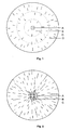
- FIG. 1 shows a schematic view of the cross section of the polycrystalline Si rod according to an embodiment of this invention.
- the polycrystalline thin rod (A) surrounded by the inner zone (B).
- FIG. 2 shows a comparison of a schematic view of the cross section of the polycrystalline Si rod according to the prior art.
- the monocrystalline thin rod (A) surrounded by single-crystal deposited silicon (B) and polycrystalline silicon (C).
- the needle crystals are shown schematically as gray, needle-shaped areas.
- FIG. 3 shows a photomicrograph (gain of 5) of the inner portion of the polycrystalline Si rod according to the present invention.
- a part of the polycrystalline thin rod (zone A) is visible in a wedge shape.
- the remainder of the picture shows the inner zone B surrounding the thin rod, in which no needle crystals are visible.
- the structure contains no separator rings.
- FIG. 4 shows a photomicrograph (gain of 5) of the outer region (zone D) of the polycrystalline Si rod according to the present invention. Needle crystals are clearly visible here as bright needles. The structure contains no separator rings.
- the molten silicon flows from the outer region (region D) into the melting zone.
- silicon is mixed so that the needle crystals melt completely and do not adversely affect the crystallization process on the monocrystalline rod.
- the needle crystals have enough time to melt since they are the largest from the outer rod portion of the polycrystalline silicon rod to the coil neck Have a way.
- the polysilicon rods according to the invention can be pulled in a single pass of the levitation melting zone in the FZ process monocrystalline and defect-free.
- the polycrystalline silicon rods according to the invention can with the diameter from 120 mm, preferably from 130, more preferably 150 to 250 mm and with the average yield of over 70% (based on the length of the thin rods used) are produced.
- Polycrystalline silicon thin rods are used as the carrier for the deposition of the polycrystalline silicon.
- the rod temperature is adjusted to 950 to 1090 ° C, preferably 1000 to 1075 ° C, more preferably 1010 to 1050 ° C.
- the hydrogen-containing Si-containing gas is injected into the reactor.
- the molar proportion of the chlorosilane compounds, preferably trichlorosilane, is then at most 30%, preferably 20 to 25%.
- the Si-containing gas decomposes on the hot rod surface, depositing the silicon.
- the gas flow is selected so that the Si deposition rate is 0.2 to 0.6 mm / h, preferably 0.25 to 0.4 mm / h.
- the rod temperature to 930 to 1030 ° C, preferably to 950 to 1020 ° C, more preferably to higher than 960 ° C and lower than 990 ° C, and converted the injected amount of hydrogen so be reduced, that the molar proportion of chlorosilanes in Switzerlandas is increased to at least 35%, but not more than 60%.
- the gas flow rate should be selected so that the Si deposition rate is 0.2 to 0.6 mm / h, preferably 0.25 to 0.4 mm / h.
- the outer region forms with the finely crystalline matrix, wherein the area ratio of the needle crystals does not exceed 7% and they are not longer than 15 mm and not wider than 2 mm.
- the lower voltages are produced at this point by these process conditions, because the rods have a lower temperature, the low hydrogen gas mixture has lower thermal conductivity, so that the rods are thermally better insulated, and the rods are exposed to lower gas flow.
- the rods according to the invention in the outer region of the fine-crystalline matrix the thermal stresses better withstand.
- the process conditions are changed from those in the inner region B to those flowing in the outer region D.
- the gas flow should be selected so that the Si deposition rate is 0.2 to 0.6 mm / h, preferably 0.25 to 0.4 mm / h.
- How to change the deposition conditions can be calculated from the time necessary for the deposition of zone C and the difference between the parameters at the end of zone B and at the beginning of zone D. The time can be determined from the thickness of zone C and the selected deposition rate.
- Deposition of the polycrystalline silicon described in this example was done according to the prior art.
- the round monocrystalline filament rods (diameter 8 mm) were exposed to the mixture of trichlorosilane (TCS) and hydrogen (molar fraction of TCS 20%).
- TCS trichlorosilane
- the bar temperature was set to 1100 ° C throughout the deposition time.
- the gas flow was controlled so that the rate of Si deposition was 0.4 mm / h.
- After reaching the diameter of 150 mm the deposition was stopped, rods were cooled, removed from the reactor and processed for zone pulling.
- the machined rods were made by ultrasonic technique, as in DE102006040486 described, checked for cracks. If the bar was cracked, the faulty area was cut off.
- the remaining piece was not shorter than 50 cm, it was passed on for FC pulling.
- the average crack-free yield in this case was only 30%, based on the length of the thin rods used.
- the rods were pulled by FZ method to the monocrystalline rods. From the processed crack-free polycrystalline Si rods only 10% could be pulled to the single crystal defect-free rods by a floating zone passage.
- the manufacturing process of the polycrystalline Si rods was carried out the same as described in Example 1, except that the molar fraction of TCS was 50%, rod temperature was controlled at 1000 ° C, and the gas flow rate was selected such that the deposition rate was 0.25 mm / h.
- the freedom from cracking was controlled as described in Example 1.
- the mean crack-free yield in this case was 75%. 30% of the polycrystalline rods used could be pulled free of defects in a single crystal in one pass of the floating zone.
- the production process of the polycrystalline Si rods was carried out analogously to Example 1, with the difference that the molar fraction of TCS was 25%, the rod temperature was controlled at 1050 ° C and the gas flow was selected so that the deposition rate 0.35 mm / h.
- the crack-free was controlled as described in Example 1. The average crack-free yield in this case was 45%. All polycrystalline rods could be pulled without defects in a single pass of the floating zone.
- the deposition of the polycrystalline silicon rods described in this example was carried out according to the present invention.
- the silicon-containing component of the reaction gas trichlorosilane was used.
- the polycrystalline Si thin rods square cross section, edge length 8 mm were used.
- the deposition was carried out at 1050 ° C with a gas mixture with the TCS content of 20%.
- the deposition rate in this step, as well as the total deposition time, was 0.35 mm / h. After the bars reached the diameter of 60 mm, the bar temperature was slowly lowered to 990 ° C and at the same time the TCS content raised to 40%. The change was slow so that it did not take place until after the bar reached the diameter of 102 mm (after 60 hours).
Landscapes
- Chemical & Material Sciences (AREA)
- Organic Chemistry (AREA)
- Engineering & Computer Science (AREA)
- Materials Engineering (AREA)
- Metallurgy (AREA)
- Inorganic Chemistry (AREA)
- Crystallography & Structural Chemistry (AREA)
- General Chemical & Material Sciences (AREA)
- Chemical Kinetics & Catalysis (AREA)
- Mechanical Engineering (AREA)
- Silicon Compounds (AREA)
- Crystals, And After-Treatments Of Crystals (AREA)
Claims (13)
- Barreau de polysilicium, pouvant être obtenu par dépôt de silicium très pur à partir d'un gaz de réaction contenant du silicium, qui a été décomposé thermiquement ou réduit par de l'hydrogène, sur un barreau filamentaire, caractérisé en ce que le barreau de polysilicium présente en section transversale radiale du barreau au moins 4 zones différentes à microstructures distinctes,a) le mince barreau polycristallin se trouvant dans la zone la plus interne A, le centre du barreau polycristallin,b) une zone B du silicium polycristallin déposé étant présente autour de ce mince barreau, dans laquelle la proportion en surface des cristaux aciculaires est inférieure à 1 %, les cristaux aciculaires ayant une longueur inférieure ou égale à 5 mm et une largeur inférieure ou égale à 1 mm,c) la proportion en surface des cristaux aciculaires dans la zone externe D du barreau de silicium polycristallin étant inférieure à 7 %, la longueur des cristaux aciculaires étant inférieure à 15 mm et la largeur des cristaux aciculaires étant inférieure à 2 mm et dans cette zone externe du barreau de silicium polycristallin la longueur des microcristaux de la matrice n'excédant pas 0,2 mm, etd) une zone mixte C étant présente entre la zone B et la zone D, dans laquelle zone mixte la structure cristalline se transforme en mode flottant de la structure dans la zone B en la structure dans la zone D.
- Barreau de polysilicium pour des applications FZ (zone flottante) pouvant être obtenu par dépôt de silicium très pur à partir d'un gaz de réaction contenant du silicium, qui a été décomposé thermiquement ou réduit par de l'hydrogène, caractérisé en ce que le barreau filamentaire est constitué de silicium polycristallin.
- Barreau de polysilicium selon les revendications 1 et 2, caractérisé en ce que le diamètre du barreau obtenu est supérieur à 120 mm.
- Barreau de polysilicium selon les revendications 1 à 3, caractérisé en ce que le barreau filamentaire présente une section transversale carrée ayant une longueur de côté de 5 à 10 mm.
- Barreau de polysilicium selon les revendications 1 à 4, caractérisé en ce que la microstructure du barreau filamentaire correspond à la microstructure de la zone B ou D.
- Barreau de polysilicium selon les revendications 1 à 5, caractérisé en ce que le diamètre de la zone B se trouvant autour du filament est au moins aussi grand que la zone de masse fondue dans le procédé FZ à utiliser ultérieurement.
- Barreau de polysilicium selon la revendication 6, caractérisé en ce que le diamètre de la zone B se trouvant autour du barreau filamentaire est supérieur à 30 mm.
- Barreau de polysilicium selon les revendications 1 à 7, caractérisé en ce que la zone externe D commence au plus tard à un diamètre de 120 mm du barreau.
- Barreau de polysilicium selon les revendications 1 à 8, caractérisé en ce que la zone mixte C résultante est constituée d'une structure cristalline qui se transforme en mode flottant de la structure dans la zone B en la structure dans la zone D.
- Barreau de polysilicium selon les revendications 1 à 9, caractérisé en ce que la section transversale du barreau ne comporte pas d'anneaux de dépôt.
- Procédé pour la fabrication d'un barreau de silicium polycristallin selon les revendications 1 à 10, comportant les étapesa.) disposition d'un corps de support sous forme d'un barreau filamentaire en silicium,b.) ajustement de la température du barreau à 950-1090 °C au début du dépôt,c.) dépôt de silicium à partir d'un gaz contenant du silicium, dilué avec de l'hydrogène, ayant une teneur molaire en les composés chlorosilane d'au maximum 30 %, le débit du gaz étant choisi de manière à ce que la vitesse de dépôt du silicium soit de 0,2 à 0,6 mm/h,d.) maintien de ces conditions jusqu'à ce que le barreau atteigne un diamètre d'au moins 30 mm, de sorte que la zone interne soit formée,e.) au plus tard après avoir atteint un diamètre du barreau de 120 mm, nouveau réglage de la température du barreau à 930-1030 °C et réduction de la quantité d'hydrogène introduite par des buses, de manière à augmenter la teneur molaire en les chlorosilanes dans le gaz entrant à au moins 35 %, mais à 60 % au maximum, et en même temps le débit du gaz est choisi pour que la vitesse de dépôt du silicium soit de 0,2 à 0,6 mm/h, de sorte que la zone externe se forme,f.) passage flottant des conditions de processus dans la fabrication de la zone interne aux conditions de processus pour la zone externe, le débit du gaz étant choisi dans ce cas de manière à ce que la vitesse de dépôt du silicium soit de 0,2 à 0,6 mm/h, etg.) aucun changement brusque des conditions de croissance pendant tout le temps du dépôt.
- Procédé selon la revendication 11, caractérisé en ce que le barreau filamentaire utilisé est constitué de silicium polycristallin.
- Procédé selon les revendications 11 et 12, caractérisé en ce que le rendement moyen est supérieur à 70 %, par rapport à la longueur du barreau filamentaire utilisé.
Applications Claiming Priority (1)
| Application Number | Priority Date | Filing Date | Title |
|---|---|---|---|
| DE102007023041A DE102007023041A1 (de) | 2007-05-16 | 2007-05-16 | Polykristalliner Siliciumstab für das Zonenziehen und ein Verfahren zu dessen Herstellung |
Publications (3)
| Publication Number | Publication Date |
|---|---|
| EP1992593A2 EP1992593A2 (fr) | 2008-11-19 |
| EP1992593A3 EP1992593A3 (fr) | 2009-03-04 |
| EP1992593B1 true EP1992593B1 (fr) | 2010-10-13 |
Family
ID=39683836
Family Applications (1)
| Application Number | Title | Priority Date | Filing Date |
|---|---|---|---|
| EP08155774A Active EP1992593B1 (fr) | 2007-05-16 | 2008-05-07 | Barreau de silicium polycristallin pour la méthode de fusion en zone flottante et son procédé de fabrication |
Country Status (7)
| Country | Link |
|---|---|
| US (1) | US7939173B2 (fr) |
| EP (1) | EP1992593B1 (fr) |
| JP (1) | JP5345341B2 (fr) |
| CN (1) | CN101311351B (fr) |
| AT (1) | ATE484486T1 (fr) |
| DE (2) | DE102007023041A1 (fr) |
| ES (1) | ES2351777T3 (fr) |
Cited By (2)
| Publication number | Priority date | Publication date | Assignee | Title |
|---|---|---|---|---|
| US12180078B2 (en) | 2019-05-21 | 2024-12-31 | Wacker Chemie Ag | Process for producing polycrystalline silicon |
| US12269747B2 (en) | 2019-06-11 | 2025-04-08 | Wacker Chemie Ag | Method for producing polycrystalline silicon |
Families Citing this family (44)
| Publication number | Priority date | Publication date | Assignee | Title |
|---|---|---|---|---|
| JP5137670B2 (ja) | 2008-04-23 | 2013-02-06 | 信越化学工業株式会社 | 多結晶シリコンロッドの製造方法 |
| CN101717990A (zh) * | 2008-10-10 | 2010-06-02 | 江西赛维Ldk太阳能高科技有限公司 | 高纯多晶硅棒作为供料棒在单晶硅区域熔炼法中的应用以及制备方法 |
| DE102008054519A1 (de) * | 2008-12-11 | 2010-06-17 | Wacker Chemie Ag | Polykristallines germaniumlegiertes Silicium und ein Verfahren zu seiner Herstellung |
| DE102009003368B3 (de) * | 2009-01-22 | 2010-03-25 | G+R Polysilicon Gmbh | Reaktor zur Herstellung von polykristallinem Silizium nach dem Monosilan-Prozess |
| EP2394955B1 (fr) * | 2009-02-04 | 2016-12-07 | Tokuyama Corporation | Procédé de production de silicium polycristallin |
| JP5751748B2 (ja) * | 2009-09-16 | 2015-07-22 | 信越化学工業株式会社 | 多結晶シリコン塊群および多結晶シリコン塊群の製造方法 |
| CN101654249B (zh) * | 2009-09-22 | 2011-04-06 | 江苏中能硅业科技发展有限公司 | 一种多晶硅硅棒的生产方法 |
| CN101746761B (zh) * | 2009-10-19 | 2011-08-24 | 洛阳金诺机械工程有限公司 | 一种硅芯熔接方法 |
| DE102010003068A1 (de) * | 2010-03-19 | 2011-09-22 | Wacker Chemie Ag | Verfahren zur Herstellung von rissfreien polykristallinen Siliciumstäben |
| DE102010040093A1 (de) | 2010-09-01 | 2012-03-01 | Wacker Chemie Ag | Verfahren zur Herstellung von polykristallinem Silicium |
| DE102010040836A1 (de) * | 2010-09-15 | 2012-03-15 | Wacker Chemie Ag | Verfahren zur Herstellung von Silicium-Dünnstäben |
| DE102010043702A1 (de) * | 2010-11-10 | 2012-05-10 | Wacker Chemie Ag | Verfahren zur Bestimmung von Verunreinigungen in Silicium |
| KR20140034260A (ko) | 2011-06-02 | 2014-03-19 | 신에쓰 가가꾸 고교 가부시끼가이샤 | 다결정 실리콘 봉의 선택 방법 및 단결정 실리콘의 제조 방법 |
| DE102011078676A1 (de) * | 2011-07-05 | 2013-01-10 | Wacker Chemie Ag | Verfahren zur Produktion von Polysilicium |
| DE102011089449A1 (de) * | 2011-12-21 | 2013-06-27 | Wacker Chemie Ag | Polykristalliner Siliciumstab und Verfahren zur Herstellung von Polysilicium |
| JP5969230B2 (ja) | 2012-03-16 | 2016-08-17 | 株式会社トクヤマ | 多結晶シリコンロッド |
| JP5828795B2 (ja) | 2012-04-04 | 2015-12-09 | 信越化学工業株式会社 | 多結晶シリコンの結晶配向度評価方法、多結晶シリコン棒の選択方法、および単結晶シリコンの製造方法 |
| DE102012207513A1 (de) | 2012-05-07 | 2013-11-07 | Wacker Chemie Ag | Polykristalliner Siliciumstab und Verfahren zu dessen Herstellung |
| DE102012207505A1 (de) | 2012-05-07 | 2013-11-07 | Wacker Chemie Ag | Polykristallines Siliciumgranulat und seine Herstellung |
| JP2014001096A (ja) | 2012-06-18 | 2014-01-09 | Shin Etsu Chem Co Ltd | 多結晶シリコンの結晶配向度評価方法、多結晶シリコン棒の選択方法、多結晶シリコン棒、多結晶シリコン塊、および、単結晶シリコンの製造方法 |
| CN111647943A (zh) * | 2012-06-29 | 2020-09-11 | 三菱综合材料株式会社 | 多晶硅棒 |
| JP5712176B2 (ja) * | 2012-08-06 | 2015-05-07 | 信越化学工業株式会社 | 多結晶シリコン棒の選択方法、多結晶シリコン塊の製造方法、及び、単結晶シリコンの製造方法 |
| DE102013207251A1 (de) | 2013-04-22 | 2014-10-23 | Wacker Chemie Ag | Verfahren zur Herstellung von polykristallinem Silicium |
| JP5947248B2 (ja) * | 2013-06-21 | 2016-07-06 | 信越化学工業株式会社 | 多結晶シリコン棒の選択方法 |
| JP5923463B2 (ja) | 2013-06-26 | 2016-05-24 | 信越化学工業株式会社 | 多結晶シリコンの結晶粒径分布の評価方法、多結晶シリコン棒の選択方法、多結晶シリコン棒、多結晶シリコン塊、および、単結晶シリコンの製造方法 |
| DE102013214799A1 (de) | 2013-07-29 | 2015-01-29 | Wacker Chemie Ag | Verfahren zur Herstellung von polykristallinem Silicium |
| CN103789827A (zh) * | 2014-01-27 | 2014-05-14 | 浙江中宁硅业有限公司 | 硅烷法生产区熔多晶硅棒的装置及方法 |
| JP6345108B2 (ja) * | 2014-12-25 | 2018-06-20 | 信越化学工業株式会社 | 多結晶シリコン棒、多結晶シリコン棒の加工方法、多結晶シリコン棒の結晶評価方法、および、fz単結晶シリコンの製造方法 |
| JP6314097B2 (ja) * | 2015-02-19 | 2018-04-18 | 信越化学工業株式会社 | 多結晶シリコン棒 |
| JP6440601B2 (ja) * | 2015-09-04 | 2018-12-19 | 信越化学工業株式会社 | 多結晶シリコン棒の製造方法およびfz単結晶シリコンの製造方法 |
| JP6416140B2 (ja) | 2016-02-12 | 2018-10-31 | 信越化学工業株式会社 | 多結晶シリコン棒および多結晶シリコン棒の選別方法 |
| JP6470223B2 (ja) | 2016-04-04 | 2019-02-13 | 信越化学工業株式会社 | 単結晶シリコンの製造方法 |
| JP2018065710A (ja) * | 2016-10-18 | 2018-04-26 | 信越化学工業株式会社 | 多結晶シリコン塊、多結晶シリコン棒、および単結晶シリコンの製造方法 |
| JP6969917B2 (ja) | 2017-07-12 | 2021-11-24 | 信越化学工業株式会社 | 多結晶シリコン棒および多結晶シリコン棒の製造方法 |
| JP6951936B2 (ja) | 2017-10-20 | 2021-10-20 | 信越化学工業株式会社 | 多結晶シリコン棒および単結晶シリコンの製造方法 |
| JP7050581B2 (ja) * | 2018-06-04 | 2022-04-08 | 信越化学工業株式会社 | 多結晶シリコンロッドの選別方法 |
| CN108622902A (zh) * | 2018-06-26 | 2018-10-09 | 昆明理工大学 | 一种提高多晶硅还原炉单炉产量的电加热装置及其方法 |
| JP7128124B2 (ja) | 2019-01-18 | 2022-08-30 | 信越化学工業株式会社 | 多結晶シリコン棒、多結晶シリコンロッドおよびその製造方法 |
| CN110133023B (zh) * | 2019-05-17 | 2022-04-26 | 西安奕斯伟材料科技有限公司 | 多晶硅选择方法、多晶硅及其在直拉法中的应用 |
| WO2020234401A1 (fr) * | 2019-05-21 | 2020-11-26 | Wacker Chemie Ag | Procédé de production de silicium polycristallin |
| JP7191780B2 (ja) | 2019-06-17 | 2022-12-19 | 信越化学工業株式会社 | 多結晶シリコンロッドの製造方法 |
| KR102618384B1 (ko) * | 2019-07-16 | 2023-12-27 | 와커 헤미 아게 | 다결정 실리콘의 제조 방법 |
| JP7247879B2 (ja) * | 2019-12-20 | 2023-03-29 | 株式会社Sumco | 単結晶シリコンウェーハの酸化膜耐圧の評価方法 |
| JP7727373B2 (ja) * | 2020-06-23 | 2025-08-21 | 信越化学工業株式会社 | 単結晶シリコンの製造方法 |
Family Cites Families (17)
| Publication number | Priority date | Publication date | Assignee | Title |
|---|---|---|---|---|
| US3540871A (en) | 1967-12-15 | 1970-11-17 | Texas Instruments Inc | Method for maintaining the uniformity of vapor grown polycrystalline silicon |
| DE2727305A1 (de) | 1977-06-16 | 1979-01-04 | Siemens Ag | Verfahren zum abscheiden von feinkristallinem silicium aus der gasphase an der oberflaeche eines erhitzten traegerkoerpers |
| DE2831816A1 (de) * | 1978-07-19 | 1980-01-31 | Siemens Ag | Verfahren zum abscheiden von silicium in feinkristalliner form |
| DE2831819A1 (de) * | 1978-07-19 | 1980-01-31 | Siemens Ag | Verfahren zum abscheiden von silicium in feinkristalliner form |
| DE3107260A1 (de) * | 1981-02-26 | 1982-09-09 | Siemens AG, 1000 Berlin und 8000 München | Verfahren und vorrichtung zum abscheiden von halbleitermaterial, insbesondere silicium |
| JP2516823B2 (ja) | 1990-02-28 | 1996-07-24 | 信越半導体株式会社 | 浮遊帯域融解法による単結晶シリコン製造用の棒状多結晶シリコン及びその製造方法 |
| CN1088444C (zh) * | 1996-05-21 | 2002-07-31 | 德山株式会社 | 多晶硅棒及其制造方法 |
| US6060021A (en) * | 1997-05-07 | 2000-05-09 | Tokuyama Corporation | Method of storing trichlorosilane and silicon tetrachloride |
| CN1077610C (zh) * | 1997-09-18 | 2002-01-09 | 中国科学院物理研究所 | 一种生长固溶体和包晶反应生成相单晶的“异成份浮区”方法 |
| US6672190B2 (en) | 2000-05-03 | 2004-01-06 | Taylor Design Group, Inc. | Precision miter gauge |
| US6676916B2 (en) * | 2001-11-30 | 2004-01-13 | Advanced Silicon Materials Llc | Method for inducing controlled cleavage of polycrystalline silicon rod |
| DE10392291B4 (de) * | 2002-02-14 | 2013-01-31 | Rec Silicon Inc. | Energie-effizientes Verfahren zum Züchten von polykristallinem Silicium |
| CN1194624C (zh) | 2003-01-20 | 2005-03-30 | 丁友昉 | 多种微生物秸秆发酵饲料与发酵剂及其制作方法 |
| JP3881647B2 (ja) * | 2003-10-07 | 2007-02-14 | 住友チタニウム株式会社 | 多結晶シリコンロッド及びその製造方法 |
| JP4328303B2 (ja) * | 2004-09-16 | 2009-09-09 | 株式会社サンリック | 太陽光発電用多結晶シリコン原料および太陽光発電用シリコンウェーハ |
| DE102004058547B4 (de) * | 2004-12-03 | 2007-10-25 | Schott Ag | Verfahren und eine Vorrichtung zur Herstellung von Einkristallen mit großem Durchmesser |
| DE102006040486A1 (de) | 2006-08-30 | 2008-03-13 | Wacker Chemie Ag | Verfahren zur zerstörungsfreien Materialprüfung von hochreinem polykristallinen Silicium |
-
2007
- 2007-05-16 DE DE102007023041A patent/DE102007023041A1/de not_active Withdrawn
-
2008
- 2008-05-07 EP EP08155774A patent/EP1992593B1/fr active Active
- 2008-05-07 AT AT08155774T patent/ATE484486T1/de active
- 2008-05-07 ES ES08155774T patent/ES2351777T3/es active Active
- 2008-05-07 DE DE502008001496T patent/DE502008001496D1/de active Active
- 2008-05-13 US US12/119,558 patent/US7939173B2/en active Active
- 2008-05-14 CN CN200810107814.XA patent/CN101311351B/zh active Active
- 2008-05-16 JP JP2008129618A patent/JP5345341B2/ja active Active
Cited By (2)
| Publication number | Priority date | Publication date | Assignee | Title |
|---|---|---|---|---|
| US12180078B2 (en) | 2019-05-21 | 2024-12-31 | Wacker Chemie Ag | Process for producing polycrystalline silicon |
| US12269747B2 (en) | 2019-06-11 | 2025-04-08 | Wacker Chemie Ag | Method for producing polycrystalline silicon |
Also Published As
| Publication number | Publication date |
|---|---|
| DE102007023041A1 (de) | 2008-11-20 |
| US20080286550A1 (en) | 2008-11-20 |
| DE502008001496D1 (de) | 2010-11-25 |
| ES2351777T3 (es) | 2011-02-10 |
| EP1992593A2 (fr) | 2008-11-19 |
| ATE484486T1 (de) | 2010-10-15 |
| JP2008285403A (ja) | 2008-11-27 |
| EP1992593A3 (fr) | 2009-03-04 |
| CN101311351A (zh) | 2008-11-26 |
| CN101311351B (zh) | 2011-08-31 |
| US7939173B2 (en) | 2011-05-10 |
| JP5345341B2 (ja) | 2013-11-20 |
Similar Documents
| Publication | Publication Date | Title |
|---|---|---|
| EP1992593B1 (fr) | Barreau de silicium polycristallin pour la méthode de fusion en zone flottante et son procédé de fabrication | |
| DE10392291B4 (de) | Energie-effizientes Verfahren zum Züchten von polykristallinem Silicium | |
| DE112013002107B4 (de) | SiC-Einkristall-Herstellungsverfahren | |
| DE102015202131B4 (de) | Verfahren zum Herstellen einer Siliziumkarbid-Halbleitervorrichtung und Siliziumkarbid-Halbleitervorrichtung | |
| DE69604235T2 (de) | Verfahren zur herstellung eines siliziumeinkristalles mit niediger fehlerdichte | |
| DE112009000328B4 (de) | Verfahren zum Aufwachsen eines Siliziumcarbideinkristalls | |
| EP1936012B1 (fr) | Procédé de fabrication de silicium cristallisé et silicium cristallisé | |
| DE112014002781T5 (de) | Sauerstoffpräzipitation in stark dotierten Siliciumwafern, geschnitten aus nach dem Czochralski-Verfahren gezüchteten Ingots | |
| DE69129709T2 (de) | Polykristalliner Silicium-Stab für das Zonenziehen und Verfahren zu seiner Herstellung | |
| DE60125472T3 (de) | SiC Material und Verfahren zu seiner Herstellung | |
| DE102009048868B4 (de) | Herstellungsverfahren für einen SiC-Volumeneinkristall mittels einer thermischen Behandlung und niederohmiges einkristallines SiC-Substrat | |
| DE69414652T2 (de) | Verbessertes Verfahren zur Bildung von Siliconkristallen | |
| DE10236023A1 (de) | Herstellungsverfahren für Silizium-Einkristallwafer und Silizium-Einkristallwafer | |
| EP2321220B1 (fr) | Procédé d'élimination d'impuretés non métalliques de silicium métallurgique | |
| DE60128544T2 (de) | Verfahren zur herstellung einer siliziumschmelze | |
| DE112016005199T5 (de) | Verfahren zur Herstellung eines Silicium-Einkristalls | |
| EP3464688B1 (fr) | Procédé de production d'une plaquette de semi-conducteur en silicium monocristallin et dispositif de production d'une plaquette de semi-conducteur en silicium monocristallin | |
| DE102004010377A1 (de) | Herstellung von Substratwafern für defektarme Halbleiterbauteile, ihre Verwendung, sowie damit erhaltene Bauteile | |
| DE112009000986T5 (de) | Einkristall-Wachstumsverfahren und Einkristall-Ziehvorrichtung | |
| DE102008013325B4 (de) | Halbleiterscheibe aus einkristallinem Silicium und Verfahren zu deren Herstellung | |
| DE112012001167T5 (de) | Silikaglastiegel, Verfahren zum Herstellen desselben und Verfahren zum Herstellen eines Silizium-Einkristalls | |
| DE112017005704T5 (de) | Verfahren zum Herstellen eines Silizium-Einkristalls und Silizium-Einkristallwafer | |
| DE112018002717B4 (de) | Verfahren zur Herstellung eines Silicium-Einkristalls | |
| AT526376B1 (de) | Verfahren zur Herstellung eines Saphir-Kristalls | |
| DE3002671A1 (de) | Verfahren zur herstellung eines siliciumcarbidsubstrats |
Legal Events
| Date | Code | Title | Description |
|---|---|---|---|
| PUAI | Public reference made under article 153(3) epc to a published international application that has entered the european phase |
Free format text: ORIGINAL CODE: 0009012 |
|
| 17P | Request for examination filed |
Effective date: 20080507 |
|
| AK | Designated contracting states |
Kind code of ref document: A2 Designated state(s): AT BE BG CH CY CZ DE DK EE ES FI FR GB GR HR HU IE IS IT LI LT LU LV MC MT NL NO PL PT RO SE SI SK TR |
|
| AX | Request for extension of the european patent |
Extension state: AL BA MK RS |
|
| PUAL | Search report despatched |
Free format text: ORIGINAL CODE: 0009013 |
|
| AK | Designated contracting states |
Kind code of ref document: A3 Designated state(s): AT BE BG CH CY CZ DE DK EE ES FI FR GB GR HR HU IE IS IT LI LT LU LV MC MT NL NO PL PT RO SE SI SK TR |
|
| AX | Request for extension of the european patent |
Extension state: AL BA MK RS |
|
| 17Q | First examination report despatched |
Effective date: 20090716 |
|
| AKX | Designation fees paid |
Designated state(s): AT BE BG CH CY CZ DE DK EE ES FI FR GB GR HR HU IE IS IT LI LT LU LV MC MT NL NO PL PT RO SE SI SK TR |
|
| GRAP | Despatch of communication of intention to grant a patent |
Free format text: ORIGINAL CODE: EPIDOSNIGR1 |
|
| GRAS | Grant fee paid |
Free format text: ORIGINAL CODE: EPIDOSNIGR3 |
|
| GRAA | (expected) grant |
Free format text: ORIGINAL CODE: 0009210 |
|
| AK | Designated contracting states |
Kind code of ref document: B1 Designated state(s): AT BE BG CH CY CZ DE DK EE ES FI FR GB GR HR HU IE IS IT LI LT LU LV MC MT NL NO PL PT RO SE SI SK TR |
|
| REG | Reference to a national code |
Ref country code: GB Ref legal event code: FG4D Free format text: NOT ENGLISH |
|
| REG | Reference to a national code |
Ref country code: CH Ref legal event code: EP |
|
| REG | Reference to a national code |
Ref country code: IE Ref legal event code: FG4D Free format text: LANGUAGE OF EP DOCUMENT: GERMAN |
|
| REF | Corresponds to: |
Ref document number: 502008001496 Country of ref document: DE Date of ref document: 20101125 Kind code of ref document: P |
|
| REG | Reference to a national code |
Ref country code: NL Ref legal event code: T3 |
|
| REG | Reference to a national code |
Ref country code: ES Ref legal event code: FG2A Effective date: 20110131 |
|
| LTIE | Lt: invalidation of european patent or patent extension |
Effective date: 20101013 |
|
| PG25 | Lapsed in a contracting state [announced via postgrant information from national office to epo] |
Ref country code: LT Free format text: LAPSE BECAUSE OF FAILURE TO SUBMIT A TRANSLATION OF THE DESCRIPTION OR TO PAY THE FEE WITHIN THE PRESCRIBED TIME-LIMIT Effective date: 20101013 Ref country code: NO Free format text: LAPSE BECAUSE OF FAILURE TO SUBMIT A TRANSLATION OF THE DESCRIPTION OR TO PAY THE FEE WITHIN THE PRESCRIBED TIME-LIMIT Effective date: 20110113 |
|
| REG | Reference to a national code |
Ref country code: IE Ref legal event code: FD4D |
|
| PG25 | Lapsed in a contracting state [announced via postgrant information from national office to epo] |
Ref country code: HR Free format text: LAPSE BECAUSE OF FAILURE TO SUBMIT A TRANSLATION OF THE DESCRIPTION OR TO PAY THE FEE WITHIN THE PRESCRIBED TIME-LIMIT Effective date: 20101013 Ref country code: PT Free format text: LAPSE BECAUSE OF FAILURE TO SUBMIT A TRANSLATION OF THE DESCRIPTION OR TO PAY THE FEE WITHIN THE PRESCRIBED TIME-LIMIT Effective date: 20110214 Ref country code: BG Free format text: LAPSE BECAUSE OF FAILURE TO SUBMIT A TRANSLATION OF THE DESCRIPTION OR TO PAY THE FEE WITHIN THE PRESCRIBED TIME-LIMIT Effective date: 20110113 Ref country code: LV Free format text: LAPSE BECAUSE OF FAILURE TO SUBMIT A TRANSLATION OF THE DESCRIPTION OR TO PAY THE FEE WITHIN THE PRESCRIBED TIME-LIMIT Effective date: 20101013 Ref country code: FI Free format text: LAPSE BECAUSE OF FAILURE TO SUBMIT A TRANSLATION OF THE DESCRIPTION OR TO PAY THE FEE WITHIN THE PRESCRIBED TIME-LIMIT Effective date: 20101013 Ref country code: IS Free format text: LAPSE BECAUSE OF FAILURE TO SUBMIT A TRANSLATION OF THE DESCRIPTION OR TO PAY THE FEE WITHIN THE PRESCRIBED TIME-LIMIT Effective date: 20110213 Ref country code: SI Free format text: LAPSE BECAUSE OF FAILURE TO SUBMIT A TRANSLATION OF THE DESCRIPTION OR TO PAY THE FEE WITHIN THE PRESCRIBED TIME-LIMIT Effective date: 20101013 Ref country code: SE Free format text: LAPSE BECAUSE OF FAILURE TO SUBMIT A TRANSLATION OF THE DESCRIPTION OR TO PAY THE FEE WITHIN THE PRESCRIBED TIME-LIMIT Effective date: 20101013 |
|
| PG25 | Lapsed in a contracting state [announced via postgrant information from national office to epo] |
Ref country code: GR Free format text: LAPSE BECAUSE OF FAILURE TO SUBMIT A TRANSLATION OF THE DESCRIPTION OR TO PAY THE FEE WITHIN THE PRESCRIBED TIME-LIMIT Effective date: 20110114 |
|
| PG25 | Lapsed in a contracting state [announced via postgrant information from national office to epo] |
Ref country code: IE Free format text: LAPSE BECAUSE OF FAILURE TO SUBMIT A TRANSLATION OF THE DESCRIPTION OR TO PAY THE FEE WITHIN THE PRESCRIBED TIME-LIMIT Effective date: 20101013 Ref country code: EE Free format text: LAPSE BECAUSE OF FAILURE TO SUBMIT A TRANSLATION OF THE DESCRIPTION OR TO PAY THE FEE WITHIN THE PRESCRIBED TIME-LIMIT Effective date: 20101013 Ref country code: CZ Free format text: LAPSE BECAUSE OF FAILURE TO SUBMIT A TRANSLATION OF THE DESCRIPTION OR TO PAY THE FEE WITHIN THE PRESCRIBED TIME-LIMIT Effective date: 20101013 |
|
| PLBE | No opposition filed within time limit |
Free format text: ORIGINAL CODE: 0009261 |
|
| STAA | Information on the status of an ep patent application or granted ep patent |
Free format text: STATUS: NO OPPOSITION FILED WITHIN TIME LIMIT |
|
| PG25 | Lapsed in a contracting state [announced via postgrant information from national office to epo] |
Ref country code: RO Free format text: LAPSE BECAUSE OF FAILURE TO SUBMIT A TRANSLATION OF THE DESCRIPTION OR TO PAY THE FEE WITHIN THE PRESCRIBED TIME-LIMIT Effective date: 20101013 Ref country code: SK Free format text: LAPSE BECAUSE OF FAILURE TO SUBMIT A TRANSLATION OF THE DESCRIPTION OR TO PAY THE FEE WITHIN THE PRESCRIBED TIME-LIMIT Effective date: 20101013 Ref country code: DK Free format text: LAPSE BECAUSE OF FAILURE TO SUBMIT A TRANSLATION OF THE DESCRIPTION OR TO PAY THE FEE WITHIN THE PRESCRIBED TIME-LIMIT Effective date: 20101013 Ref country code: PL Free format text: LAPSE BECAUSE OF FAILURE TO SUBMIT A TRANSLATION OF THE DESCRIPTION OR TO PAY THE FEE WITHIN THE PRESCRIBED TIME-LIMIT Effective date: 20101013 |
|
| REG | Reference to a national code |
Ref country code: NO Ref legal event code: RE |
|
| REG | Reference to a national code |
Ref country code: NO Ref legal event code: T2 Effective date: 20101013 |
|
| 26N | No opposition filed |
Effective date: 20110714 |
|
| PGRI | Patent reinstated in contracting state [announced from national office to epo] |
Ref country code: NO Effective date: 20110831 |
|
| REG | Reference to a national code |
Ref country code: DE Ref legal event code: R097 Ref document number: 502008001496 Country of ref document: DE Effective date: 20110714 |
|
| BERE | Be: lapsed |
Owner name: WACKER CHEMIE A.G. Effective date: 20110531 |
|
| PG25 | Lapsed in a contracting state [announced via postgrant information from national office to epo] |
Ref country code: MC Free format text: LAPSE BECAUSE OF NON-PAYMENT OF DUE FEES Effective date: 20110531 Ref country code: MT Free format text: LAPSE BECAUSE OF FAILURE TO SUBMIT A TRANSLATION OF THE DESCRIPTION OR TO PAY THE FEE WITHIN THE PRESCRIBED TIME-LIMIT Effective date: 20101013 |
|
| PG25 | Lapsed in a contracting state [announced via postgrant information from national office to epo] |
Ref country code: BE Free format text: LAPSE BECAUSE OF NON-PAYMENT OF DUE FEES Effective date: 20110531 |
|
| REG | Reference to a national code |
Ref country code: CH Ref legal event code: PL |
|
| GBPC | Gb: european patent ceased through non-payment of renewal fee |
Effective date: 20120507 |
|
| PG25 | Lapsed in a contracting state [announced via postgrant information from national office to epo] |
Ref country code: CH Free format text: LAPSE BECAUSE OF NON-PAYMENT OF DUE FEES Effective date: 20120531 Ref country code: LI Free format text: LAPSE BECAUSE OF NON-PAYMENT OF DUE FEES Effective date: 20120531 |
|
| PG25 | Lapsed in a contracting state [announced via postgrant information from national office to epo] |
Ref country code: GB Free format text: LAPSE BECAUSE OF NON-PAYMENT OF DUE FEES Effective date: 20120507 |
|
| PG25 | Lapsed in a contracting state [announced via postgrant information from national office to epo] |
Ref country code: CY Free format text: LAPSE BECAUSE OF FAILURE TO SUBMIT A TRANSLATION OF THE DESCRIPTION OR TO PAY THE FEE WITHIN THE PRESCRIBED TIME-LIMIT Effective date: 20101013 Ref country code: LU Free format text: LAPSE BECAUSE OF NON-PAYMENT OF DUE FEES Effective date: 20110507 |
|
| PG25 | Lapsed in a contracting state [announced via postgrant information from national office to epo] |
Ref country code: TR Free format text: LAPSE BECAUSE OF FAILURE TO SUBMIT A TRANSLATION OF THE DESCRIPTION OR TO PAY THE FEE WITHIN THE PRESCRIBED TIME-LIMIT Effective date: 20101013 |
|
| PG25 | Lapsed in a contracting state [announced via postgrant information from national office to epo] |
Ref country code: HU Free format text: LAPSE BECAUSE OF FAILURE TO SUBMIT A TRANSLATION OF THE DESCRIPTION OR TO PAY THE FEE WITHIN THE PRESCRIBED TIME-LIMIT Effective date: 20101013 |
|
| REG | Reference to a national code |
Ref country code: AT Ref legal event code: MM01 Ref document number: 484486 Country of ref document: AT Kind code of ref document: T Effective date: 20130507 |
|
| PG25 | Lapsed in a contracting state [announced via postgrant information from national office to epo] |
Ref country code: AT Free format text: LAPSE BECAUSE OF NON-PAYMENT OF DUE FEES Effective date: 20130507 |
|
| REG | Reference to a national code |
Ref country code: FR Ref legal event code: PLFP Year of fee payment: 9 |
|
| REG | Reference to a national code |
Ref country code: FR Ref legal event code: PLFP Year of fee payment: 10 |
|
| REG | Reference to a national code |
Ref country code: FR Ref legal event code: PLFP Year of fee payment: 11 |
|
| PGFP | Annual fee paid to national office [announced via postgrant information from national office to epo] |
Ref country code: NL Payment date: 20190521 Year of fee payment: 12 |
|
| PGFP | Annual fee paid to national office [announced via postgrant information from national office to epo] |
Ref country code: PL Payment date: 20190404 Year of fee payment: 12 Ref country code: ES Payment date: 20190621 Year of fee payment: 12 |
|
| PGFP | Annual fee paid to national office [announced via postgrant information from national office to epo] |
Ref country code: FR Payment date: 20190523 Year of fee payment: 12 |
|
| REG | Reference to a national code |
Ref country code: NL Ref legal event code: MM Effective date: 20200601 |
|
| PG25 | Lapsed in a contracting state [announced via postgrant information from national office to epo] |
Ref country code: NL Free format text: LAPSE BECAUSE OF NON-PAYMENT OF DUE FEES Effective date: 20200601 |
|
| PG25 | Lapsed in a contracting state [announced via postgrant information from national office to epo] |
Ref country code: FR Free format text: LAPSE BECAUSE OF NON-PAYMENT OF DUE FEES Effective date: 20200531 |
|
| REG | Reference to a national code |
Ref country code: ES Ref legal event code: FD2A Effective date: 20210928 |
|
| PG25 | Lapsed in a contracting state [announced via postgrant information from national office to epo] |
Ref country code: IT Free format text: LAPSE BECAUSE OF NON-PAYMENT OF DUE FEES Effective date: 20200507 |
|
| PG25 | Lapsed in a contracting state [announced via postgrant information from national office to epo] |
Ref country code: ES Free format text: LAPSE BECAUSE OF NON-PAYMENT OF DUE FEES Effective date: 20200508 |
|
| P01 | Opt-out of the competence of the unified patent court (upc) registered |
Effective date: 20230502 |
|
| REG | Reference to a national code |
Ref country code: DE Ref legal event code: R081 Ref document number: 502008001496 Country of ref document: DE Owner name: WACKER CHEMIE AG, DE Free format text: FORMER OWNER: WACKER CHEMIE AG, 81737 MUENCHEN, DE |
|
| PGFP | Annual fee paid to national office [announced via postgrant information from national office to epo] |
Ref country code: DE Payment date: 20250521 Year of fee payment: 18 |
|
| PGFP | Annual fee paid to national office [announced via postgrant information from national office to epo] |
Ref country code: NO Payment date: 20250523 Year of fee payment: 18 |