EP1993148A1 - Optische sende-/empfangseinrichtung - Google Patents
Optische sende-/empfangseinrichtung Download PDFInfo
- Publication number
- EP1993148A1 EP1993148A1 EP07714226A EP07714226A EP1993148A1 EP 1993148 A1 EP1993148 A1 EP 1993148A1 EP 07714226 A EP07714226 A EP 07714226A EP 07714226 A EP07714226 A EP 07714226A EP 1993148 A1 EP1993148 A1 EP 1993148A1
- Authority
- EP
- European Patent Office
- Prior art keywords
- light
- wire
- base substrate
- receiving device
- optical transmitting
- Prior art date
- Legal status (The legal status is an assumption and is not a legal conclusion. Google has not performed a legal analysis and makes no representation as to the accuracy of the status listed.)
- Withdrawn
Links
Images



Classifications
-
- H—ELECTRICITY
- H10—SEMICONDUCTOR DEVICES; ELECTRIC SOLID-STATE DEVICES NOT OTHERWISE PROVIDED FOR
- H10F—INORGANIC SEMICONDUCTOR DEVICES SENSITIVE TO INFRARED RADIATION, LIGHT, ELECTROMAGNETIC RADIATION OF SHORTER WAVELENGTH OR CORPUSCULAR RADIATION
- H10F77/00—Constructional details of devices covered by this subclass
-
- H—ELECTRICITY
- H10—SEMICONDUCTOR DEVICES; ELECTRIC SOLID-STATE DEVICES NOT OTHERWISE PROVIDED FOR
- H10F—INORGANIC SEMICONDUCTOR DEVICES SENSITIVE TO INFRARED RADIATION, LIGHT, ELECTROMAGNETIC RADIATION OF SHORTER WAVELENGTH OR CORPUSCULAR RADIATION
- H10F77/00—Constructional details of devices covered by this subclass
- H10F77/50—Encapsulations or containers
-
- A—HUMAN NECESSITIES
- A61—MEDICAL OR VETERINARY SCIENCE; HYGIENE
- A61B—DIAGNOSIS; SURGERY; IDENTIFICATION
- A61B5/00—Measuring for diagnostic purposes; Identification of persons
- A61B5/02—Detecting, measuring or recording for evaluating the cardiovascular system, e.g. pulse, heart rate, blood pressure or blood flow
- A61B5/024—Measuring pulse rate or heart rate
- A61B5/0245—Measuring pulse rate or heart rate by using sensing means generating electric signals, i.e. ECG signals
-
- A—HUMAN NECESSITIES
- A61—MEDICAL OR VETERINARY SCIENCE; HYGIENE
- A61B—DIAGNOSIS; SURGERY; IDENTIFICATION
- A61B5/00—Measuring for diagnostic purposes; Identification of persons
- A61B5/02—Detecting, measuring or recording for evaluating the cardiovascular system, e.g. pulse, heart rate, blood pressure or blood flow
- A61B5/026—Measuring blood flow
- A61B5/0261—Measuring blood flow using optical means, e.g. infrared light
-
- H—ELECTRICITY
- H01—ELECTRIC ELEMENTS
- H01S—DEVICES USING THE PROCESS OF LIGHT AMPLIFICATION BY STIMULATED EMISSION OF RADIATION [LASER] TO AMPLIFY OR GENERATE LIGHT; DEVICES USING STIMULATED EMISSION OF ELECTROMAGNETIC RADIATION IN WAVE RANGES OTHER THAN OPTICAL
- H01S5/00—Semiconductor lasers
- H01S5/02—Structural details or components not essential to laser action
- H01S5/0206—Substrates, e.g. growth, shape, material, removal or bonding
- H01S5/0207—Substrates having a special shape
-
- H—ELECTRICITY
- H01—ELECTRIC ELEMENTS
- H01S—DEVICES USING THE PROCESS OF LIGHT AMPLIFICATION BY STIMULATED EMISSION OF RADIATION [LASER] TO AMPLIFY OR GENERATE LIGHT; DEVICES USING STIMULATED EMISSION OF ELECTROMAGNETIC RADIATION IN WAVE RANGES OTHER THAN OPTICAL
- H01S5/00—Semiconductor lasers
- H01S5/02—Structural details or components not essential to laser action
- H01S5/022—Mountings; Housings
- H01S5/023—Mount members, e.g. sub-mount members
- H01S5/02325—Mechanically integrated components on mount members or optical micro-benches
-
- H—ELECTRICITY
- H01—ELECTRIC ELEMENTS
- H01S—DEVICES USING THE PROCESS OF LIGHT AMPLIFICATION BY STIMULATED EMISSION OF RADIATION [LASER] TO AMPLIFY OR GENERATE LIGHT; DEVICES USING STIMULATED EMISSION OF ELECTROMAGNETIC RADIATION IN WAVE RANGES OTHER THAN OPTICAL
- H01S5/00—Semiconductor lasers
- H01S5/02—Structural details or components not essential to laser action
- H01S5/022—Mountings; Housings
- H01S5/0233—Mounting configuration of laser chips
- H01S5/02345—Wire-bonding
-
- H—ELECTRICITY
- H01—ELECTRIC ELEMENTS
- H01S—DEVICES USING THE PROCESS OF LIGHT AMPLIFICATION BY STIMULATED EMISSION OF RADIATION [LASER] TO AMPLIFY OR GENERATE LIGHT; DEVICES USING STIMULATED EMISSION OF ELECTROMAGNETIC RADIATION IN WAVE RANGES OTHER THAN OPTICAL
- H01S5/00—Semiconductor lasers
- H01S5/02—Structural details or components not essential to laser action
- H01S5/022—Mountings; Housings
- H01S5/0235—Method for mounting laser chips
- H01S5/02355—Fixing laser chips on mounts
- H01S5/0237—Fixing laser chips on mounts by soldering
-
- H—ELECTRICITY
- H10—SEMICONDUCTOR DEVICES; ELECTRIC SOLID-STATE DEVICES NOT OTHERWISE PROVIDED FOR
- H10W—GENERIC PACKAGES, INTERCONNECTIONS, CONNECTORS OR OTHER CONSTRUCTIONAL DETAILS OF DEVICES COVERED BY CLASS H10
- H10W72/00—Interconnections or connectors in packages
- H10W72/071—Connecting or disconnecting
- H10W72/073—Connecting or disconnecting of die-attach connectors
-
- H—ELECTRICITY
- H10—SEMICONDUCTOR DEVICES; ELECTRIC SOLID-STATE DEVICES NOT OTHERWISE PROVIDED FOR
- H10W—GENERIC PACKAGES, INTERCONNECTIONS, CONNECTORS OR OTHER CONSTRUCTIONAL DETAILS OF DEVICES COVERED BY CLASS H10
- H10W72/00—Interconnections or connectors in packages
- H10W72/50—Bond wires
- H10W72/531—Shapes of wire connectors
- H10W72/536—Shapes of wire connectors the connected ends being ball-shaped
-
- H—ELECTRICITY
- H10—SEMICONDUCTOR DEVICES; ELECTRIC SOLID-STATE DEVICES NOT OTHERWISE PROVIDED FOR
- H10W—GENERIC PACKAGES, INTERCONNECTIONS, CONNECTORS OR OTHER CONSTRUCTIONAL DETAILS OF DEVICES COVERED BY CLASS H10
- H10W72/00—Interconnections or connectors in packages
- H10W72/50—Bond wires
- H10W72/531—Shapes of wire connectors
- H10W72/5363—Shapes of wire connectors the connected ends being wedge-shaped
-
- H—ELECTRICITY
- H10—SEMICONDUCTOR DEVICES; ELECTRIC SOLID-STATE DEVICES NOT OTHERWISE PROVIDED FOR
- H10W—GENERIC PACKAGES, INTERCONNECTIONS, CONNECTORS OR OTHER CONSTRUCTIONAL DETAILS OF DEVICES COVERED BY CLASS H10
- H10W72/00—Interconnections or connectors in packages
- H10W72/50—Bond wires
- H10W72/551—Materials of bond wires
- H10W72/552—Materials of bond wires comprising metals or metalloids, e.g. silver
-
- H—ELECTRICITY
- H10—SEMICONDUCTOR DEVICES; ELECTRIC SOLID-STATE DEVICES NOT OTHERWISE PROVIDED FOR
- H10W—GENERIC PACKAGES, INTERCONNECTIONS, CONNECTORS OR OTHER CONSTRUCTIONAL DETAILS OF DEVICES COVERED BY CLASS H10
- H10W72/00—Interconnections or connectors in packages
- H10W72/851—Dispositions of multiple connectors or interconnections
- H10W72/874—On different surfaces
- H10W72/884—Die-attach connectors and bond wires
-
- H—ELECTRICITY
- H10—SEMICONDUCTOR DEVICES; ELECTRIC SOLID-STATE DEVICES NOT OTHERWISE PROVIDED FOR
- H10W—GENERIC PACKAGES, INTERCONNECTIONS, CONNECTORS OR OTHER CONSTRUCTIONAL DETAILS OF DEVICES COVERED BY CLASS H10
- H10W90/00—Package configurations
Definitions
- the present invention relates to an optical transmitting and receiving device which is used mainly as a blood flow sensor for measuring a blood flow volume and the like.
- a blood flowmeter including a semiconductor substrate formed in its surface with recesses in which a light emitting element and a photodetecting element are disposed, respectively, and a cover substrate disposed on the surface of the semiconductor substrate and formed with a light shielding film (see Patent Document 1, for example).
- a light emitting element is electrically connected with an electrode formed on an inner surface of the recess via a wire.
- Patent Document 1 Japanese Published Unexamined Patent Application No. 2004-229920
- such an optical transmitting and receiving device has the following problem. That is, since one terminal electrode of the light emitting element is electrically connected with an electrode formed on an inner surface of the recess via a wire, it becomes necessary to provide a space to store the wire in the recess, so that the recess is increased in size by that space. Therefore, this hinders downsizing of the semiconductor substrate, and moreover, hinders downsizing of the optical transmitting and receiving device.
- the present invention has been made in view of such circumstances, and it is an object to provide an optical transmitting and receiving device that can be downsized.
- an optical transmitting and receiving device includes: a light emitting element for emitting light forward; a photodetecting element for receiving light irradiated from the front; a base substrate formed at a front surface thereof with a first recess in which the light emitting element is disposed and a second recess in which the photodetecting element is disposed; a light shielding member disposed at a front-surface side of the base substrate and formed with a first light passing hole through which light emitted by the light emitting element passes and a second light passing hole through which light to be received by the photodetecting element passes; and a light transmitting member which is disposed at a front-surface side of the light shielding member and through which light emitted by the light emitting element and light to be received by the photodetecting element are transmitted, wherein at least one of terminal electrodes of the light emitting element and terminal electrodes of the photodetecting element is electrically connected, via a wire, with a wiring formed on the front surface of the base substrate
- an optical transmitting and receiving device includes: a light emitting element for emitting light forward; a photodetecting element for receiving light irradiated from the front; a base substrate formed at a front surface thereof with a recess in which the light emitting element and the photodetecting element are disposed; a light shielding member disposed at a front-surface side of the base substrate and formed with a first light passing hole through which light emitted by the light emitting element passes and a second light passing hole through which light to be received by the photodetecting element passes; and a light transmitting member which is disposed at a front-surface side of the light shielding member and through which light emitted by the light emitting element and light to be received by the photodetecting element are transmitted, wherein at least one of terminal electrodes of the light emitting element and terminal electrodes of the photodetecting element is electrically connected, via a wire, with a wiring formed on the front surface of the base substrate, and in the light shielding member, a wire storing portion to store the wire is formed.
- At least one of terminal electrodes of the light emitting element and terminal electrodes of the photodetecting element is electrically connected, via a wire, with a wiring formed on the front surface of the base substrate, and in the light shielding member disposed at a front-surface side of the base substrate, a wire storing portion to store the wire is formed. Since this makes it no longer necessary to provide a space to store the wire in the recess, it becomes possible to downsize the recess. Accordingly, it becomes possible not only to downsize the base substrate but also to downsize the optical transmitting and receiving device.
- the wire storing portion to store the wire electrically connected with at least one of the terminal electrodes of the light emitting element is a recess or a through-hole.
- the wire storing portion can be simply formed.
- the wire storing portion to store the wire electrically connected with at least one of the terminal electrodes of the light emitting element is a through-hole, and this through-hole and the first light passing hole are continuously formed.
- the wire storing portion can be further simply formed.
- the wire storing portion to store the wire electrically connected with at least one of the terminal electrodes of the photodetecting element is a recess.
- the wire storing portion can be simply formed, and light irradiated from the front can be prevented from being received by the wire storing portion via the wire storing portion.
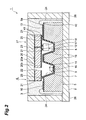
- 1... optical transmitting and receiving device 5 ... base substrate, 5a ... front surface, 7 ... first cavity (first recess), 8 ... second cavity (second recess), 9 ... LD (light emitting element), 12 ... PD (photodetecting element), 15, 16 ... LD terminal electrode, 17, 18 ... PD terminal electrode, 19 ... base substrate wiring portion (wiring), 20 ... light shielding member, 22 ... opening (first light passing hole), 23 ... pinhole (second light passing hole), 27 ... light transmitting member, 28, 31 ... wire, 29, 32 ... wire storing portion , 33 ... cavity (recess).
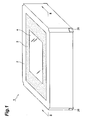
- an optical transmitting and receiving device 1 includes an enclosure 2 formed of, for example, a plastic material, in a rectangular-parallelepiped cup shape opened forward.
- a main body portion 4 which incorporates an LD (light emitting element) 9 that emits light forward and a PD (photodetecting element) that receives light irradiated from the front, and around the main body portion 4 in the enclosure 2, filled is, for example, an insulating-coated, light shielding resin 3 made of a silicone resin containing a carbon filler.
- This optical transmitting and receiving device 1 is used as, for example, a blood flow sensor that detects a blood flow in a body tissue and measures a blood flow volume, a blood flow velocity, a pulse, and the like by means of scattered light scattered by irradiating light on the body tissue.
- the main body portion 4 has a base substrate 5 at a bottom-surface side in the enclosure 2.
- This base substrate 5 is formed of, for example, silicon being a semiconductor material, in a rectangular plate shape with a width of 2.8mm, a length of 6.0mm, and a thickness of 1.0mm, and in a front surface 5a of the base substrate 5, formed is a recess-like first cavity (first recess) 7 and second cavity (second recess) 8.
- the LD 9 is disposed in the first cavity 7, and is electrically connected with an LD anode 10 and an LD cathode 11 to be described later.
- the PD 12 is disposed in the second cavity 8, and is electrically connected with a PD anode 13 and a PD cathode 14 to be described later.
- the cavity 7, 8 is formed by, for example, applying wet etching to a silicon substrate to be the base substrate 5.
- the cavity 7, 8 is formed by providing, on the surface of a silicon substrate to be the base substrate 5, a mask formed of SiN or the like to demarcate the shape of the cavity 7, 8 and making an etchant act on an opening of this mask. After etching, the SiN mask is removed, and an insulating film 40 with a thickness of 1.5 ⁇ m and made of, for example, SiO 2 is then formed on, at least, the surface of the cavity and the surface of the substrate by thermal oxidation.
- the LD 9 uses, for example, a VCSEL (vertical-cavity surface-emitting laser) made of a compound semiconductor material with a thickness of 0.2mm, and this emits light having a wavelength of 850nm.
- a VCSEL vertical-cavity surface-emitting laser
- an LD terminal electrode 15 is provided at the front end face
- an LD terminal electrode 16 is provided at the rear end face.
- the PD 12 uses, for example, a Si-PD or GaAs-PD made of a semiconductor material with a thickness of 0.3mm.
- a PD terminal electrode 17 and a PD terminal electrode 18 are provided at the front end face.
- the material of the PD 12 is selected according to the wavelength of light to be emitted by the LD 9. For example, when the wavelength of light to be emitted by the LD 9 is 780nm, Si or GaAs is used as the material of the PD 12, and when the wavelength of light to be emitted by the LD 9 is 1.31 ⁇ m, InGaAs is used as the material of the PD 12.
- a base substrate wiring portion (wiring) 19 with a predetermined pattern On the insulating film 40 on the front surface 5a of the base substrate 5 and the inner surface of the cavity 7, 8, formed by, for example, an A1 film, a Ti-Pt-Au laminated film, or a Cr-Pt-Au laminated film is a base substrate wiring portion (wiring) 19 with a predetermined pattern.
- This base substrate wiring portion 19 has an LD anode 10 and an LD cathode 11 on the first cavity 7 side and has a PD anode 13 and a PD cathode 14 on the second cavity 8 side.
- the LD anode 10, LD cathode 11, PD anode 13, and PD cathode 14 are, as shown in Fig. 1 and Fig.
- the LD terminal electrode 16 of the LD 9 is electrically connected via, for example, a solder, a conductive resin, or the like.
- a light shielding member 20 formed of, for example, a silicon substrate coated with an insulating film 41 made of SiO 2 in a rectangular plate shape with a thickness of 0.15mm to 0.30mm, and this is fixed by bump bonding 21.
- the material for the bump bonding 21 include Au, Ni, Cu, AuSn, and SnAg-based solders.
- a light shielding portion may be formed by applying or filling a light shielding material.
- the light shielding member 20 formed is an opening (first light passing hole) 22 provided at a position corresponding to the first cavity 7 and a pinhole (second light passing hole) 23 provided at a position corresponding to the second cavity 8.
- the opening 22 guides light emitted from the LD 9 to the outside.
- the pinhole 23 guides scattered light from the outside to the PD 12 and also prevents ambient light and unnecessary light from the outside from entering the PD 12.
- the opening 22 and the pinhole 23 are formed by, for example, applying dry etching to a silicon substrate to be the light shielding member 20, and the pinhole 23 has a high aspect ratio.
- the pinhole 23 is formed at a position corresponding to a photodetecting surface of the PD 12, and the diameter thereof is provided as, for example, 30 ⁇ m to 90 ⁇ m. This is because noise due to ambient light and unnecessary light from the outside to be sensed by the PD 12 is increased when the diameter of the pinhole 23 is larger than 90 ⁇ m, while when the diameter of the pinhole 23 is smaller than 30 ⁇ m, light to be received by the PD 12 is reduced, so that an output from the PD 12 is lowered.
- a light shielding member wiring portion 25 is formed with a predetermined pattern, and this is electrically connected with the base substrate wiring portion 19 by bump bonding 21.
- the PD terminal electrode 17, 18 of the PD 12 is electrically connected (so-called, flip-chip bonding) by bump bonding 21.
- the PD 12 is electrically connected with each of the PD anode 13 and PD cathode 14.
- a light transmitting member 27 formed of, for example, alkali-containing borosilicate glass in a rectangular plate shape with a thickness of 0.3mm so that light emitted from the LD 9 and scattered light from the outside are transmitted therethrough, and this is fixed by a resin.
- This light transmitting member 27 enhances mechanical strength of the light shielding member 20 and also seals the first cavity 7 and the second cavity 8 of the base substrate 5 into a package.
- the coefficient of thermal expansion of the light transmitting member 27 and the coefficient of thermal expansion of the light shielding member 20 are set almost equal.
- the light shielding member 20 and the light transmitting member 27 may be fixed by anodic bonding. When anodic bonding is performed, the insulating film 41 is no longer necessary on the light transmitting member 27 side.
- the LD terminal electrode 15 of the LD 9 is electrically connected, via a wire 28, to the base substrate wiring portion 19 formed on the insulating film 40 on the front surface 5a of the base substrate 5.
- a wire storing portion 29 is formed in the light shielding member 20 laminated on and fixed to the front surface 5a side of the base substrate 5. Since these make it no longer necessary to provide a space to store the wire 28 in the first cavity 7, it becomes possible to downsize the first cavity 7. Accordingly, it becomes possible not only to downsize the base substrate 5 but also to downsize the optical transmitting and receiving device 1.
- the wire storing portion 29 to store the wire 28 is a through-hole, and this through-hole and the opening 22 are continuously formed. Adopting such a construction allows simply forming the wire storing portion 29 along with the opening 22.
- a part of the scattered light thus scattered advances in a direction opposite the forward direction of the light emitted from the LD 9, is transmitted through the light transmitting member 27, passes through the pinhole 23 formed in the light shielding member 20, and reaches the PD 12 disposed in the second cavity 8 of the base substrate 5. Then, a voltage signal in response to the reached light is obtained from the PD anode 13 and the PD cathode 14 of the base substrate wiring portion 19.
- the scattered light contains an interference component between scattered light from a stationary body tissue and scattered light that has received a Doppler shift from red blood cells moving in the capillaries of a body tissue, a frequency analysis of the voltage signal obtained by the PD 12 enables blood flow measurements etc.
- the optical transmitting and receiving device 1 according to a second embodiment differs in the shape of the wire storing portion 29 from the optical transmitting and receiving device 1 according to the first embodiment. More specifically, in the optical transmitting and receiving device 1 according to the second embodiment, as shown in Fig. 5 , the wire storing portion 29 is provided as a recess formed on the rear surface 20b of the light shielding member 20, and is formed continuously with the opening 22.
- optical transmitting and receiving device 1 according to the second embodiment constructed as such also provides the same operations and effects as those of the optical transmitting and receiving device 1 according to the first embodiment.
- the optical transmitting and receiving device 1 according to a third embodiment differs in the construction of the PD 12 from the optical transmitting and receiving device 1 according to the first embodiment. More specifically, in the optical transmitting and receiving device 1 according to the third embodiment, as shown in Fig. 6 and Fig. 7 , the PD terminal electrode 17 is provided at the front end face of the PD 12 and the PD terminal electrode 18 is provided at the rear end face of the PD 12. And, the PD terminal electrode 17 is electrically connected, via a wire 31, with the base substrate wiring portion 19 formed on the insulating film 40 on the front surface 5a of the base substrate 5, and the PD terminal electrode 18 is electrically connected with the base substrate wiring portion 19 formed on the insulating film 40 on the bottom surface of the second cavity 8.
- the wire storing portion 32 On the rear surface 20b of the light shielding member 20, formed as a recess is a wire storing portion 32 to store the wire 31, and the wire storing portion 32 is formed continuously with the pinhole 23. Also, in consideration of ambient light and unnecessary light that enter the PD 12, the length of the pinhole 23 is provided as 0.1mm or more.
- optical transmitting and receiving device 1 according to the third embodiment constructed as such also provides the same operations and effects as those of the optical transmitting and receiving device 1 according to the first embodiment.
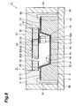
- the optical transmitting and receiving device 1 according to the fourth embodiment differs in the shape of the base substrate 5 from the optical transmitting and receiving device 1 according to the first embodiment. More specifically, in the optical transmitting and receiving device 1 according to the fourth embodiment, as shown in Fig. 8 and Fig. 9 , a cavity (recess) 33 in which the LD 9 and the PD 12 are disposed is formed in the front surface 5a of the base substrate 5. Between the light shielding member 20 and the PD 12, a light shielding portion 34 made of a light shielding resin is provided so as to surround a photodetecting surface 12a of the PD 12. This prevents ambient light and unnecessary light from entering the PD 12 due to light emission or the like of the LD 9.
- optical transmitting and receiving device 1 according to the fourth embodiment constructed as such also provides the same operations and effects as those of the optical transmitting and receiving device 1 according to the first embodiment.
- an optical transmitting and receiving device may be constructed such that a wire electrically connected with the LD terminal electrode of an LD is stored in a wire storing portion which is a recess formed in the rear surface of a light shielding member and a wire electrically connected with the PD terminal electrode of a PD is stored in a wire storing portion which is a recess formed in the rear surface of a light shielding member.
- an optical transmitting and receiving device may be constructed such that an LD formed at the front end face with an anode-side LD terminal electrode and a cathode-side LD terminal electrode is electrically connected by flip-chip bonding with a light shielding member wiring portion formed on an insulating film on the rear surface of a light shielding member and a wire electrically connected with the PD terminal electrode of a PD is stored in a wire storing portion which is a recess formed in the rear surface of the light shielding member.
- the through-hole may be formed discontinuously with the opening (that is, independently of the opening).
- the recess may be formed discontinuously with the opening or pinhole (that is, independently of the opening or pinhole).
Landscapes
- Health & Medical Sciences (AREA)
- Life Sciences & Earth Sciences (AREA)
- Engineering & Computer Science (AREA)
- Cardiology (AREA)
- Molecular Biology (AREA)
- General Health & Medical Sciences (AREA)
- Physiology (AREA)
- Biophysics (AREA)
- Pathology (AREA)
- Biomedical Technology (AREA)
- Heart & Thoracic Surgery (AREA)
- Medical Informatics (AREA)
- Veterinary Medicine (AREA)
- Surgery (AREA)
- Animal Behavior & Ethology (AREA)
- Physics & Mathematics (AREA)
- Public Health (AREA)
- Hematology (AREA)
- Signal Processing (AREA)
- Light Receiving Elements (AREA)
- Semiconductor Lasers (AREA)
- Measuring Pulse, Heart Rate, Blood Pressure Or Blood Flow (AREA)
- Optical Integrated Circuits (AREA)
- Led Device Packages (AREA)
- Photo Coupler, Interrupter, Optical-To-Optical Conversion Devices (AREA)
Applications Claiming Priority (2)
| Application Number | Priority Date | Filing Date | Title |
|---|---|---|---|
| JP2006047249A JP4708214B2 (ja) | 2006-02-23 | 2006-02-23 | 光送受信デバイス |
| PCT/JP2007/052696 WO2007097240A1 (ja) | 2006-02-23 | 2007-02-15 | 光送受信デバイス |
Publications (2)
| Publication Number | Publication Date |
|---|---|
| EP1993148A1 true EP1993148A1 (de) | 2008-11-19 |
| EP1993148A4 EP1993148A4 (de) | 2010-12-22 |
Family
ID=38437278
Family Applications (1)
| Application Number | Title | Priority Date | Filing Date |
|---|---|---|---|
| EP07714226A Withdrawn EP1993148A4 (de) | 2006-02-23 | 2007-02-15 | Optische sende-/empfangseinrichtung |
Country Status (7)
| Country | Link |
|---|---|
| US (1) | US20090202251A1 (de) |
| EP (1) | EP1993148A4 (de) |
| JP (1) | JP4708214B2 (de) |
| KR (1) | KR20080100332A (de) |
| CN (1) | CN101371373B (de) |
| TW (1) | TWI398969B (de) |
| WO (1) | WO2007097240A1 (de) |
Cited By (4)
| Publication number | Priority date | Publication date | Assignee | Title |
|---|---|---|---|---|
| EP2745772A4 (de) * | 2011-08-19 | 2015-09-16 | Murata Manufacturing Co | Sensor für lebende organismen |
| KR20180072766A (ko) * | 2016-01-25 | 2018-06-29 | 쿄세라 코포레이션 | 계측 센서용 패키지 및 계측 센서 |
| EP3395242A4 (de) * | 2015-12-22 | 2019-09-04 | KYOCERA Corporation | Messsensorpaket und messsensor |
| EP3745090A1 (de) * | 2019-05-27 | 2020-12-02 | Dr. Johannes Heidenhain GmbH | Lichtquelle sowie verfahren zu deren herstellung und positionsmesseinrichtung mit einer lichtquelle |
Families Citing this family (27)
| Publication number | Priority date | Publication date | Assignee | Title |
|---|---|---|---|---|
| JP4943739B2 (ja) * | 2006-05-18 | 2012-05-30 | 浜松ホトニクス株式会社 | 光送受信デバイス |
| JP5031894B2 (ja) * | 2008-05-12 | 2012-09-26 | パイオニア株式会社 | 自発光型センサ装置 |
| KR101064072B1 (ko) | 2009-02-24 | 2011-09-08 | 엘지이노텍 주식회사 | 발광 소자 패키지 |
| CN102375185B (zh) * | 2010-08-20 | 2013-11-13 | 国碁电子(中山)有限公司 | 光收发器及其制造方法 |
| JP5709165B2 (ja) * | 2011-03-10 | 2015-04-30 | セイコーインスツル株式会社 | 光学デバイス |
| JP5692390B2 (ja) | 2011-08-19 | 2015-04-01 | 株式会社村田製作所 | 生体センサ |
| US8675706B2 (en) * | 2011-12-24 | 2014-03-18 | Princeton Optronics Inc. | Optical illuminator |
| US9981844B2 (en) * | 2012-03-08 | 2018-05-29 | Infineon Technologies Ag | Method of manufacturing semiconductor device with glass pieces |
| CN107369728B (zh) * | 2012-08-30 | 2019-07-26 | 京瓷株式会社 | 受光发光元件以及使用该受光发光元件的传感器装置 |
| JP6229338B2 (ja) * | 2013-07-12 | 2017-11-15 | セイコーエプソン株式会社 | 光検出ユニット及び生体情報検出装置 |
| USD724548S1 (en) * | 2013-09-13 | 2015-03-17 | Citizen Electronics Co., Ltd. | Light-emitting diode |
| USD724039S1 (en) * | 2013-09-13 | 2015-03-10 | Citizen Electronics Co., Ltd. | Light-emitting diode |
| WO2016092680A1 (ja) * | 2014-12-11 | 2016-06-16 | 愛知時計電機株式会社 | 血流センサ |
| EP3440998B1 (de) * | 2016-04-04 | 2022-11-16 | Kyocera Corporation | Messsensorpaket und messsensor |
| JP6631423B2 (ja) * | 2016-07-04 | 2020-01-15 | オムロン株式会社 | 生体情報検知装置および生体情報検知装置を備える椅子 |
| US20180017741A1 (en) * | 2016-07-15 | 2018-01-18 | Advanced Semiconductor Engineering, Inc. | Semiconductor package device and method of manufacturing the same |
| JP6718339B2 (ja) * | 2016-09-06 | 2020-07-08 | 京セラ株式会社 | 計測センサ用パッケージおよび計測センサ |
| JP6891441B2 (ja) * | 2016-10-12 | 2021-06-18 | セイコーエプソン株式会社 | 検出装置および測定装置 |
| WO2018153464A1 (en) * | 2017-02-23 | 2018-08-30 | Osram Opto Semiconductors Gmbh | Sensor element |
| JP6735463B2 (ja) * | 2017-03-24 | 2020-08-05 | 愛知時計電機株式会社 | 計測装置 |
| US11255770B2 (en) | 2018-01-30 | 2022-02-22 | Kyocera Corporation | Measurement apparatus |
| WO2019208165A1 (ja) * | 2018-04-24 | 2019-10-31 | ソニー株式会社 | 散乱光信号計測装置及び情報処理装置 |
| WO2020090883A1 (ja) * | 2018-10-30 | 2020-05-07 | 京セラ株式会社 | 光学センサ装置 |
| US20210401300A1 (en) * | 2018-11-12 | 2021-12-30 | Sony Group Corporation | Biological information measuring device |
| US12201396B2 (en) * | 2021-09-10 | 2025-01-21 | Rockley Photonics Limited | Optical speckle receiver |
| US12484796B1 (en) | 2024-11-27 | 2025-12-02 | Rockley Photonics Limited | System and method for measuring pulse wave velocity |
| US12396648B1 (en) | 2024-11-27 | 2025-08-26 | Rockley Photonics Limited | Wearable device with light source and optical sensor |
Family Cites Families (9)
| Publication number | Priority date | Publication date | Assignee | Title |
|---|---|---|---|---|
| EP0489177A4 (en) * | 1990-06-26 | 1993-06-09 | Seiko Epson Corporation | Semiconductor device and method of manufacturing the same |
| JP3161142B2 (ja) * | 1993-03-26 | 2001-04-25 | ソニー株式会社 | 半導体装置 |
| JP2002117702A (ja) * | 2000-10-11 | 2002-04-19 | Toyoda Gosei Co Ltd | 光源装置 |
| US6574254B1 (en) * | 2002-02-08 | 2003-06-03 | Harvatek Corp. | Laser diode package with heat sinking substrate |
| JP3627186B2 (ja) * | 2002-06-17 | 2005-03-09 | 光磊科技股▲ふん▼有限公司 | 半導体発光装置のパッケージに用いられる熱放散構造とその製造方法 |
| US6646290B1 (en) * | 2002-08-23 | 2003-11-11 | Amkor Technology, Inc. | Optical structure having an optical diode and a sensor in separate apertures inside double insulating layers |
| JP3882756B2 (ja) * | 2003-01-30 | 2007-02-21 | 日本電信電話株式会社 | 血流計のセンサ部及び血流計 |
| JP2004242166A (ja) * | 2003-02-07 | 2004-08-26 | Seiko Epson Corp | 光モジュール及びその製造方法並びに電子機器 |
| JP2006013174A (ja) * | 2004-06-25 | 2006-01-12 | Kyocera Corp | 光半導体装置 |
-
2006
- 2006-02-23 JP JP2006047249A patent/JP4708214B2/ja not_active Expired - Fee Related
-
2007
- 2007-02-15 US US12/280,116 patent/US20090202251A1/en not_active Abandoned
- 2007-02-15 CN CN2007800030575A patent/CN101371373B/zh not_active Expired - Fee Related
- 2007-02-15 WO PCT/JP2007/052696 patent/WO2007097240A1/ja not_active Ceased
- 2007-02-15 KR KR1020087011109A patent/KR20080100332A/ko not_active Withdrawn
- 2007-02-15 EP EP07714226A patent/EP1993148A4/de not_active Withdrawn
- 2007-02-16 TW TW096105954A patent/TWI398969B/zh not_active IP Right Cessation
Cited By (11)
| Publication number | Priority date | Publication date | Assignee | Title |
|---|---|---|---|---|
| EP2745772A4 (de) * | 2011-08-19 | 2015-09-16 | Murata Manufacturing Co | Sensor für lebende organismen |
| EP3053519A1 (de) * | 2011-08-19 | 2016-08-10 | Murata Manufacturing Co., Ltd. | Biosensor |
| US9439569B2 (en) | 2011-08-19 | 2016-09-13 | Murata Manufacturing Co., Ltd. | Biosensor having light emitting and receiving elements to obtain a biological signal |
| US10111592B2 (en) | 2011-08-19 | 2018-10-30 | Murata Manufacturing Co., Ltd. | Biosensor |
| EP3395242A4 (de) * | 2015-12-22 | 2019-09-04 | KYOCERA Corporation | Messsensorpaket und messsensor |
| CN112168146A (zh) * | 2015-12-22 | 2021-01-05 | 京瓷株式会社 | 测量传感器用封装体以及测量传感器 |
| EP4026493A1 (de) * | 2015-12-22 | 2022-07-13 | Kyocera Corporation | Messsensorpaket und messsensor |
| KR20180072766A (ko) * | 2016-01-25 | 2018-06-29 | 쿄세라 코포레이션 | 계측 센서용 패키지 및 계측 센서 |
| EP3410127A4 (de) * | 2016-01-25 | 2019-08-28 | Kyocera Corporation | Messsensorpaket und messsensor |
| US11717178B2 (en) | 2016-01-25 | 2023-08-08 | Kyocera Corporation | Measurement sensor package and measurement sensor |
| EP3745090A1 (de) * | 2019-05-27 | 2020-12-02 | Dr. Johannes Heidenhain GmbH | Lichtquelle sowie verfahren zu deren herstellung und positionsmesseinrichtung mit einer lichtquelle |
Also Published As
| Publication number | Publication date |
|---|---|
| JP4708214B2 (ja) | 2011-06-22 |
| CN101371373B (zh) | 2011-04-27 |
| KR20080100332A (ko) | 2008-11-17 |
| JP2007225923A (ja) | 2007-09-06 |
| EP1993148A4 (de) | 2010-12-22 |
| CN101371373A (zh) | 2009-02-18 |
| TW200802971A (en) | 2008-01-01 |
| US20090202251A1 (en) | 2009-08-13 |
| TWI398969B (zh) | 2013-06-11 |
| WO2007097240A1 (ja) | 2007-08-30 |
Similar Documents
| Publication | Publication Date | Title |
|---|---|---|
| EP1993148A1 (de) | Optische sende-/empfangseinrichtung | |
| EP3566075B1 (de) | Vcsel-näherungssensor mit enger konvergenz | |
| JP4586337B2 (ja) | 半導体レーザモジュールおよび半導体レーザ装置 | |
| US8777496B2 (en) | Optical device | |
| JP2005167189A (ja) | 光−電気変換モジュール及びそれを用いた光トランシーバ | |
| JP5206944B2 (ja) | 光学モジュールおよびそれを用いた医療用光計測システム | |
| JPWO2019189630A1 (ja) | 流量流速算出装置、流量流速センサ装置、流量装置および流量流速算出方法 | |
| CN101529600B (zh) | 光接收发送装置 | |
| JP2018170454A (ja) | 光半導体装置 | |
| JP2017131286A (ja) | 計測センサ用パッケージおよび計測センサ | |
| JP6718339B2 (ja) | 計測センサ用パッケージおよび計測センサ | |
| KR20180012210A (ko) | 광 반도체 장치 | |
| JP4454233B2 (ja) | 光パッケージ及びそれを用いた光モジュール | |
| JP7054609B2 (ja) | 計測センサ用パッケージ及び計測センサ | |
| JP6462904B2 (ja) | 計測センサ用パッケージおよび計測センサ | |
| JP2000323791A (ja) | 垂直共振器型面発光レーザと光検出用モニターとのアセンブリー及びそのアセンブリング方法 | |
| JP6753729B2 (ja) | 計測センサ用パッケージおよび計測センサ | |
| US20210401300A1 (en) | Biological information measuring device | |
| JPS62169488A (ja) | 光電子装置 | |
| JPS62169487A (ja) | 光電子装置 | |
| JP2004207620A (ja) | 光通信用パッケージ |
Legal Events
| Date | Code | Title | Description |
|---|---|---|---|
| PUAI | Public reference made under article 153(3) epc to a published international application that has entered the european phase |
Free format text: ORIGINAL CODE: 0009012 |
|
| 17P | Request for examination filed |
Effective date: 20080821 |
|
| AK | Designated contracting states |
Kind code of ref document: A1 Designated state(s): DE FR GB |
|
| DAX | Request for extension of the european patent (deleted) | ||
| RBV | Designated contracting states (corrected) |
Designated state(s): DE FR GB |
|
| A4 | Supplementary search report drawn up and despatched |
Effective date: 20101124 |
|
| 17Q | First examination report despatched |
Effective date: 20101210 |
|
| STAA | Information on the status of an ep patent application or granted ep patent |
Free format text: STATUS: THE APPLICATION IS DEEMED TO BE WITHDRAWN |
|
| 18D | Application deemed to be withdrawn |
Effective date: 20110421 |