EP1993194A1 - Signal comparison circuit and power conversion device - Google Patents
Signal comparison circuit and power conversion device Download PDFInfo
- Publication number
- EP1993194A1 EP1993194A1 EP07715035A EP07715035A EP1993194A1 EP 1993194 A1 EP1993194 A1 EP 1993194A1 EP 07715035 A EP07715035 A EP 07715035A EP 07715035 A EP07715035 A EP 07715035A EP 1993194 A1 EP1993194 A1 EP 1993194A1
- Authority
- EP
- European Patent Office
- Prior art keywords
- circuit
- value
- integration
- signal
- current
- Prior art date
- Legal status (The legal status is an assumption and is not a legal conclusion. Google has not performed a legal analysis and makes no representation as to the accuracy of the status listed.)
- Withdrawn
Links
- 238000006243 chemical reaction Methods 0.000 title description 16
- 230000010354 integration Effects 0.000 claims abstract description 161
- 238000001514 detection method Methods 0.000 claims abstract description 64
- 230000007274 generation of a signal involved in cell-cell signaling Effects 0.000 claims abstract description 49
- 238000005259 measurement Methods 0.000 abstract description 3
- 230000003111 delayed effect Effects 0.000 abstract 1
- 238000011156 evaluation Methods 0.000 abstract 1
- 238000010586 diagram Methods 0.000 description 12
- 239000003990 capacitor Substances 0.000 description 5
- 239000000203 mixture Substances 0.000 description 5
- 239000000872 buffer Substances 0.000 description 4
- 239000000126 substance Substances 0.000 description 4
- 230000001934 delay Effects 0.000 description 3
- 230000001447 compensatory effect Effects 0.000 description 1
- 230000000694 effects Effects 0.000 description 1
- 238000009499 grossing Methods 0.000 description 1
- 238000005070 sampling Methods 0.000 description 1
Images




Classifications
-
- H—ELECTRICITY
- H02—GENERATION; CONVERSION OR DISTRIBUTION OF ELECTRIC POWER
- H02M—APPARATUS FOR CONVERSION BETWEEN AC AND AC, BETWEEN AC AND DC, OR BETWEEN DC AND DC, AND FOR USE WITH MAINS OR SIMILAR POWER SUPPLY SYSTEMS; CONVERSION OF DC OR AC INPUT POWER INTO SURGE OUTPUT POWER; CONTROL OR REGULATION THEREOF
- H02M3/00—Conversion of DC power input into DC power output
- H02M3/22—Conversion of DC power input into DC power output with intermediate conversion into AC
- H02M3/24—Conversion of DC power input into DC power output with intermediate conversion into AC by static converters
- H02M3/28—Conversion of DC power input into DC power output with intermediate conversion into AC by static converters using discharge tubes with control electrode or semiconductor devices with control electrode to produce the intermediate AC
- H02M3/325—Conversion of DC power input into DC power output with intermediate conversion into AC by static converters using discharge tubes with control electrode or semiconductor devices with control electrode to produce the intermediate AC using devices of a triode or a transistor type requiring continuous application of a control signal
- H02M3/335—Conversion of DC power input into DC power output with intermediate conversion into AC by static converters using discharge tubes with control electrode or semiconductor devices with control electrode to produce the intermediate AC using devices of a triode or a transistor type requiring continuous application of a control signal using semiconductor devices only
-
- H—ELECTRICITY
- H02—GENERATION; CONVERSION OR DISTRIBUTION OF ELECTRIC POWER
- H02M—APPARATUS FOR CONVERSION BETWEEN AC AND AC, BETWEEN AC AND DC, OR BETWEEN DC AND DC, AND FOR USE WITH MAINS OR SIMILAR POWER SUPPLY SYSTEMS; CONVERSION OF DC OR AC INPUT POWER INTO SURGE OUTPUT POWER; CONTROL OR REGULATION THEREOF
- H02M3/00—Conversion of DC power input into DC power output
- H02M3/02—Conversion of DC power input into DC power output without intermediate conversion into AC
- H02M3/04—Conversion of DC power input into DC power output without intermediate conversion into AC by static converters
- H02M3/10—Conversion of DC power input into DC power output without intermediate conversion into AC by static converters using discharge tubes with control electrode or semiconductor devices with control electrode
- H02M3/145—Conversion of DC power input into DC power output without intermediate conversion into AC by static converters using discharge tubes with control electrode or semiconductor devices with control electrode using devices of a triode or transistor type requiring continuous application of a control signal
- H02M3/155—Conversion of DC power input into DC power output without intermediate conversion into AC by static converters using discharge tubes with control electrode or semiconductor devices with control electrode using devices of a triode or transistor type requiring continuous application of a control signal using semiconductor devices only
- H02M3/156—Conversion of DC power input into DC power output without intermediate conversion into AC by static converters using discharge tubes with control electrode or semiconductor devices with control electrode using devices of a triode or transistor type requiring continuous application of a control signal using semiconductor devices only with automatic control of output voltage or current, e.g. switching regulators
- H02M3/157—Conversion of DC power input into DC power output without intermediate conversion into AC by static converters using discharge tubes with control electrode or semiconductor devices with control electrode using devices of a triode or transistor type requiring continuous application of a control signal using semiconductor devices only with automatic control of output voltage or current, e.g. switching regulators with digital control
-
- H—ELECTRICITY
- H02—GENERATION; CONVERSION OR DISTRIBUTION OF ELECTRIC POWER
- H02M—APPARATUS FOR CONVERSION BETWEEN AC AND AC, BETWEEN AC AND DC, OR BETWEEN DC AND DC, AND FOR USE WITH MAINS OR SIMILAR POWER SUPPLY SYSTEMS; CONVERSION OF DC OR AC INPUT POWER INTO SURGE OUTPUT POWER; CONTROL OR REGULATION THEREOF
- H02M3/00—Conversion of DC power input into DC power output
- H02M3/02—Conversion of DC power input into DC power output without intermediate conversion into AC
- H02M3/04—Conversion of DC power input into DC power output without intermediate conversion into AC by static converters
- H02M3/10—Conversion of DC power input into DC power output without intermediate conversion into AC by static converters using discharge tubes with control electrode or semiconductor devices with control electrode
- H02M3/145—Conversion of DC power input into DC power output without intermediate conversion into AC by static converters using discharge tubes with control electrode or semiconductor devices with control electrode using devices of a triode or transistor type requiring continuous application of a control signal
- H02M3/155—Conversion of DC power input into DC power output without intermediate conversion into AC by static converters using discharge tubes with control electrode or semiconductor devices with control electrode using devices of a triode or transistor type requiring continuous application of a control signal using semiconductor devices only
Definitions
- the present invention concerns to the power converter that has the signal comparison circuit generating a target signal from the analog quantity and the digital quantity, the comparison circuit.
- the power converter can on-off control the current that flows from DC power aiming at the inductor in high accuracy by using the current limit circuit based on the deflection between the output voltage value and the target output voltage value that the output voltage detection circuit detected, and can digitalized the controll operation circuit.
- Electric power conversion device 9 of the current inject type shown in Figure 19 (DC/DC converter) is known so far.
- This electric power conversion device 9 consists of the control circuit 91, the driving circuit 92 and the converter circuit 93.
- the converter circuit 93 consists of the power supply E i , the transistor switch T r , the resistance R s for detecting current, the inductor L, the flywheel diode F D , and the output capacitor C.
- the control circuit 91 detects the current that flows in output voltage e o and the inductor L as voltage down e s of the resistance R s .
- the control circuit 91 controls input current i i by operating the transistor switch Tr on-off so that e o may approach e o * (deflection must become 0), referring to the value of voltage down e s .
- the comparator compares peak voltage e p and voltage Vs (it is generated with putting preset gain A cc on voltage descent e s ). And, the comparison result is input to the flip-flop FF circuit that operates by driving signal S s (sampling cycle T s ). As a result, control signal S c of which the duty is the time to reaching to the peak voltage e p is generated.
- the driving circuit 92 controls transistor switch T r based on this control signal S c .
- the response accuracy of electric power conversion circuit 9 of Figure 19 depends on the resolution of control signal S C as shown in Figure 20 .
- the frequency of the practicable oscillator used for the electric power conversion circuit 9 is 100MHz now. Therefore, the response accuracy of electric power conversion circuit 9 is bad
- the purpose of the present invention is to be able to on-off control the current that flows from the power supply aiming at the inductor in high accuracy and to digitalize the control operation circuit.
- the voltage detection circuit has been digitalized. Therefore, various operation quantity signals are generable.
- the other integration start time of two integration circuits used for the current control is shifted.
- This shift time is an quantity that corresponds to deflection, and resolution is high. Therefore, high accuracy is controlled.
- the current peak is suppressed in high accuracy. Therefore, when input (Ei) of DC power is unstable, the present invention is suitable.
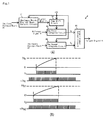
- Figure 1(A) is a composition diagram wherein an execution form of the comparison of signals of the present invention circuit is shown.
- the signal comparison circuit 8 consists of "analog quantity/digital quantity conversion circuit" 81, the operation signal generation circuit 82, the first integration circuit 83, the second integration circuit 84, and a target signal output circuit 85 in Figure 1(A) .
- the analog quantity/digital quantity conversion circuit 81 generates the digital quantity D(digital signal) from the first analog quantity A1(analog signal).
- the conversion circuit 81 can execute the operation processing ( of the digital filter processing etc.) to digital quantity D.
- the circuit for generating the time operation signal generating circuit" 82 shifts the operation start timing of the first integration circuit to the operation start timing of the second integration circuit by changing the digital quantity into the time quantity.
- the first integration circuit 83 inputs the reference signal R and outputs the integration value S 1 .
- the second integration circuit 84 inputs the second analog quantity A2 and outputs the integration value S 2 .
- the signal comparison circuit 85 compares the time until the first integration circuit 83 reaches the sreshold value and the time until the second integration circuit 84 reaches the sreshold value
- the analog quantity/digital quantity conversion circuit 81, the circuit 82 the first integration circuit 83 and the second integration circuit 84 can be operated with the clock of integral multiples of clock clk on substance by multi-phase processing reference clock clk.Or,that is, N clocks are generated from the reference clock, wherein the frequency of said N clocks are the same with the clock of the reference clock clk.
- the first clock delays only Tp/N for the reference clock, the second clock delays only 2Tp/N for the reference clock,..., and the Nth clock delays only(N-1)TP/N.
- These delay signals is synthesized, and a new high resolution clock is formed. High-speed operation can be done by adopting this synthetic signal as the new clock.
- Figure 1(B) shows the reference signal R(The threshold is shown with THR), the integration value S 1 , the clock clk R sped up, the second analog quantity A 2 (the threshold value is shown as TH A2 ), the integration value S 2 , and the clock clk A2 sped up.
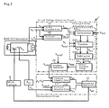
- FIG. 1 and Figure 2 are the explanation diagrams where the power converter of the present invention is shown.
- the electric power converter 1 has output voltage detection circuit 2, current control circuit 3, and DC/DC conversion circuit 4.
- the current control circuit 3 controls the circuit current of the DC/DC conversion circuit 4(current ii that flows from DC power Ei aiming at reactor L) by on/off switching, based on the deflection between the output voltage e o detected by the output voltage detection circuit 2 and the target output voltage e o * .
- the DC/DC conversion circuit 4 has the DC power Ei, the transistor switch Tr, the current detection resistance Rs, the inductor L, the flywheel diode FD, and output capacitor C.
- the current (electric power) supplied from power supply (DC power)Ei is supplied to the load R through the current detection resistance Rs and the inductor L.
- the flywheel diode FD turns on when the transistor switch T r is turned off, and supplies the energy that accumulates in inductor L to load R.
- Output capacitor C is a smoothing capacitor.
- the output voltage detection circuit 2 has the first integration circuit (for the voltage detection) 21, the second integration circuit (for the armature voltage control) 22, the output deflection detection circuit 23, the control operate circuit 24 and the operation quantity signal generation circuit 25.
- the first integration circuit 21 (for the voltage detection) inputs the output voltage e o according to the timing of the first clock S s and outputs the first integration value (for the voltage detection) S eo .
- the secon integration circuit 22 (for the voltage detection) inputs the output voltage e o * according to the timing of the first clock S s and outputs the second integration value (for the voltage detection) S eo * .
- the first integration circuit (for voltage detection)21 and the second integration circuit 22 (for voltage control)22 can be composed by the capacitor and resistance.
- the first clock Ss is sped up as shown in Figure 4(A) and (B) , wheerin the standard clock P is shifted .
- TP/N Tp are a cycle of P, N is integer("4" in Figure 4(A) )).
- the delay x can shift the operation timing of these circuits 211,212 only at preset time (TP/N). As a result, the accuracy of the voltage detection rises, and operation is sped up.
- the operation timing of integration circuit 221,222 is shifted by delay x only at preset time (TP/N). As a result, the accuracy of the voltage control rises, and operation is sped up.
- the operation timing of these integration circuits 221,222 is shifted by delay x only at preset time (TP/N). As a result, the accuracy of the voltage detection (and control) can be raised and operation be sped up.
- the output deflection detection circuit 23 consists of the comparator 231, the counter 232, and the subtracter 233.
- the comparator 231 compares the time until the first integration value (for voltage detection) Seo reaches to the preset value Vth v1 and the time until the second integration value (for voltage detection) Seo* reaches to the preset value Vth v2
- the counter 232 counts the time Neo (the time until the first integration value S eo reaches to threshold Vth v ) and the time Neo* (the time until the second integration value S eo * reaches to threshold Vth v ), by calucrating the pulse number of pulses of clocks Ssmp1 as shown Figure 6 .
- Subtracter 233 caluclates the difference ⁇ NR using the pulse number of the clocks (for voltage deflection detection) Ssmp1, and outputs the differ between the voltage value e o and the target output voltage value e eo * as the degital deflection value ⁇ NR.
- the control operation circuit 24 inputs digital deflection value ⁇ NR, and generates numerical value N RM digital to control the current control circuit 3 based on this value ⁇ NR.
- the clock Ssmp1 is one by one cycle T e (one cycle of on-off of transistor switch Tr) of the first clock S e (Numerical value NRM for controling the current control circuit 3 is detected one time, or more time).
- two or more pulses P1, P2, P3, and P4 can preset comparatively shift to reference pulse P0 in 1/N(1/4 in the example). As a result, it can be N times (4 times in the example) at the cycle of reference pulse TP as for driving cycle P on substance.
- the peration quantity signal generation circuit 25 generates the operation quantity signal that changed the timing of the reference clock signal (reference signal Ssmp2) at time.
- This time quantity of the change is the time corresponding to a digital numerical value that corresponds to the target output voltage e o of the output voltage eo * and deflection.
- the resolution of this time quantity of the change is higher than the frequency of a reference clock.
- the operation quantity signal generation circuit 25 inputs the signal (reference signal Ssmp2) that becomes a reference of the time of operation in numerical value NRM digital and current control circuit 3.
- the operation quantity signal generation circuit 25 generates operation quantity signal Ssmp3 as shown in Figure 9 .
- This operation quantity signal Ssmp3 is a signal that changed standing up of signal Ssmp2 at time only at time corresponding to numerical value NRM digital.
- the frequency of signal Ssmp2 is 25MHz
- the resolution of time change ⁇ t is 25GHz.
- the operation quantity signal generation circuit 25 comprises the decoder 251 and the delay circuit 252.
- the decoder 251 inputs numerical value N RM , and outputs two or more bit signal S RM .
- the delay circuit 252 inputs the signal S RM and the reference signal S smp2 .
- the circuit of Figure 11(A) is a delay circuit that used two or more buffers.
- This delay circuit generates signal (S 1 ,5 2 , ⁇ ) with the delay time.
- the delay time depends on the buffer number that signal S0 passes. Or instance, when numerical value NRM (digital value) is Q bit, the delay signal of 2 Q kind of is prepared.
- These delay signals are signals to delay clock S smp2 .
- the numerical value N RM is converted into signal S RM with the decoder 251. An arbitrary delay can be generated by selecting the buffer corresponding to this S RM .
- the buffer number can be assumed to be about 1000. Therefore, it is generally operation quantity signal Ssmp3 with 1000 times resolution accuracy (25GHz), if the clock Ssmp2 is 25MHz.
- Figure 12(A) shows other composition examples of the operation quantity signal generation circuit 25.
- the operation quantity signal generation circuit 25 of Figure 12(A) is composed of the digital-to-analog converter 255, the integration circuit 256, and the comparator 257.
- the digital-to-analog converter 255 inputs a digital numerical value to the control current control circuit 3, and outputs the analog sreshold voltage.
- the ntegration circuit 256 inputs the reference signal S smp2 and the outputs the integration value voltage S L .
- the comparator 257 outputs the comparison value of the integration value voltage and the analog sreshold voltage.
- the numerical value NRM digital is set to threshold voltage V th by converting D/A.
- about 25GHz can compose the operation quantity signal generation circuit 25 of the counter.
- the current control circuit 3 has the first integration circuit (for the current control) 31, the second integration circuit (for the current control) 32, and current control signal generation circuit 33.
- the first integration circuit (for the current control) 31 inputs preset value ec according to the timing of standing up of operation quantity signal Ssmp3 and outputs the first integration value (for the current control) Sep for the current control.
- the second integration circuit (for the current control) 32 inputs the voltage Vs according to the timing (Here, timing of Ssmp2) that synchronizes with standing up of the reference clock S smp4 (reference signal), and outputs the second integration value (for the current control) S Vs .
- Voltage V s is a voltage in which preset gain A cc is put on voltage e s that corresponds to the current that flows in the inductor L.
- the current control signal generation circuit 33 compares the first integration value (for the current control) S ep and the second integration value (for the current control) S Vs in this execution form with analog.
- the current control signal generation circuit 33 can sample the first integration value (for the current control) S ep and the second integration value SVs with a clock with the resolution of time change ⁇ t, and compare these integration values.
- the current control signal generation circuit 33 can be composed of the comparison circuit 331 and off the signal generation circuit 332 as shown in Figure 13 for instance.
- Figure 14 shows the timing chart of the operation of current control signal generation circuit 33.
- the circuit 331 consists of the comparator 3311,3312 and AND gate 3313.
- the comparison Comparator 3311 compares the first integration value Sep (for the current control) and the first preset value V th3 , and outputs the comparison result as S ep _ edg .
- the comparator 3312 compares the second integration value S Vs (for the current control) and the second preset value V th4 , and outputs the comparison result as SV s_edg . In Figure 14 , it is the same value V thc as prest value V th3 and V th4 .
- the off signal generation circuit 332 is composed by two FF circuits 3321, 3322 in Figure 13 .
- FF circuit 3321 generates current control signal S off following the time to reaching to the second preset value V th4 (It is Vthc here) by the second integration value (for the current control) S Vs the time until the first integration value (for the current control) S ep reaches to the first preset value V th3 (it is Vthc, in this embodiment)
- the current control signal S off turns off the current i i that flows from the DC power E i aiming at the inductor L.
- the set value e c is input to the first integration circuit (for the current control) 31 at each cycle of the clock S ssmp2 (Or, S smp3 ) and the reference clock S smp4 .
- the voltage V s is input to the second integration circuit(for the current control) 32, integrated respectively, and converted into the signal S Vs and S ep .
- the voltage V s (voltage in which gain A cc is put on the voltage e s that corresponds to the current that flows in inductor L) is input to the first integration circuit 31 for the current control.
- the current control signal S off is generated when this input value reaches the integration value of preset value e c , and the transistor switch Tr is turned off (refer to the timing chart for Figure 15 ).
- two or more the operation quantity signal generation circuits (25) can be moutet(in this embodiment, three circuits shown by 251,252,253). In Figure 16(A) , the detection accuracy aises and the operation was sped up.
- Figure 16(B) shows a concrete composition of operation quantity signal generation circuit 25.
- the eference clock S amp2 diverges to the plural as shown in Figure 16(B) .
- the delay signal is caused by each delay element selected with selector Y, and outputs as S amp2 .
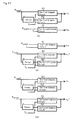
- Figure 17(A), (B), and (C) are the diagrams where the example of the design change of the power converter mentioned.
- Figure 17(A) shows the example of raising the detection accuracy and speeding up operation by two or more sets (two Figures 17(A) ) mounting the first integration circuit (for the current control ) 31.
- Ssmp3 input to the first integration circuit (for the current control) 311 and the first integration circuit 312 for the current control is late for Ssmp3 input to the first integration circuit (for the current control) 311 at 1/2 cycles.
- Figure 17(B) shows the first integration circuit 31 for the current control and the second integration circuit 32 for the current control and the installing example of two or more classes (two Figures 17(B) ) is shown.
- Ssmp4 input to the second integration circuit (for the current control) 321 is late for Ssmp4 input to the second integration circuit (for the current control) 322 at 1/2 cycles.
- the first integration circuit (for the current control) 31 and the second integration circuit (for the current control) 32 show the installing example of two or more classes (two Figures 17(A) ) in Figure 17(C) .
- Ssmp3 input to the first integration circuit (for the current control) 311 and the first integration circuit (for the current control) 312 is late for Ssmp3 input to the first integration circuit 311 for the current control at 1/2 cycles.
- Ssmp4 input to the second integration circuit 321 for the current control is late for Ssmp4 input to the second integration circuit 322 for the current control at 1/2 cycles.
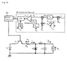
- the value that inputs NMR to peak value setting circuit 71 as shown in Figure 18(B) and corresponds to the peak value can be output.
- Ssmp4 and voltage Vs are input to integration circuit 72 (for the current control), and train of impulses SS is output, and on the other hand, this is done with counter 73 and several in total can be done.
- circuit in the present invention is superior to the circuit described in Figure 18(A) and (B) from reliability and the viewpoint of high speed etc.
Landscapes
- Engineering & Computer Science (AREA)
- Power Engineering (AREA)
- Dc-Dc Converters (AREA)
- Analogue/Digital Conversion (AREA)
- Inverter Devices (AREA)
Applications Claiming Priority (2)
| Application Number | Priority Date | Filing Date | Title |
|---|---|---|---|
| JP2006044499 | 2006-02-21 | ||
| PCT/JP2007/053710 WO2007097465A1 (ja) | 2006-02-21 | 2007-02-21 | 信号比較回路および電力変換装置 |
Publications (1)
| Publication Number | Publication Date |
|---|---|
| EP1993194A1 true EP1993194A1 (en) | 2008-11-19 |
Family
ID=38437500
Family Applications (1)
| Application Number | Title | Priority Date | Filing Date |
|---|---|---|---|
| EP07715035A Withdrawn EP1993194A1 (en) | 2006-02-21 | 2007-02-21 | Signal comparison circuit and power conversion device |
Country Status (5)
| Country | Link |
|---|---|
| US (1) | US8089257B2 (ko) |
| EP (1) | EP1993194A1 (ko) |
| JP (1) | JP5039977B2 (ko) |
| KR (1) | KR101388127B1 (ko) |
| WO (1) | WO2007097465A1 (ko) |
Families Citing this family (5)
| Publication number | Priority date | Publication date | Assignee | Title |
|---|---|---|---|---|
| JP5417640B2 (ja) * | 2009-02-28 | 2014-02-19 | 国立大学法人 長崎大学 | 信号発生装置 |
| JP5509624B2 (ja) * | 2009-02-28 | 2014-06-04 | 国立大学法人 長崎大学 | 信号発生装置 |
| US9448274B2 (en) * | 2014-04-16 | 2016-09-20 | Teradyne, Inc. | Circuitry to protect a test instrument |
| JP7024440B2 (ja) * | 2018-01-24 | 2022-02-24 | 富士電機株式会社 | 電力変換装置の制御回路、及び、電力変換装置 |
| WO2020109914A1 (en) * | 2018-11-28 | 2020-06-04 | Silanna Asia Pte Ltd | Digitally compensated current sensing protection |
Family Cites Families (5)
| Publication number | Priority date | Publication date | Assignee | Title |
|---|---|---|---|---|
| JP2005006391A (ja) * | 2003-06-11 | 2005-01-06 | Shindengen Electric Mfg Co Ltd | Dc−dcコンバータ |
| JP3957682B2 (ja) | 2003-12-19 | 2007-08-15 | シャープ株式会社 | スイッチング電源装置及びそれを用いた電子機器 |
| JP4829622B2 (ja) * | 2005-02-17 | 2011-12-07 | キヤノン株式会社 | スイッチング電源、スイッチング電源を備えた電子機器、スイッチング電源を備えた記録装置 |
| JP4613986B2 (ja) * | 2008-07-28 | 2011-01-19 | 日本テキサス・インスツルメンツ株式会社 | スイッチング電源装置 |
| JP2011035948A (ja) * | 2009-07-29 | 2011-02-17 | Fujitsu Semiconductor Ltd | Dc−dcコンバータ、制御回路及び電源電圧制御方法 |
-
2007
- 2007-02-21 JP JP2008501788A patent/JP5039977B2/ja active Active
- 2007-02-21 EP EP07715035A patent/EP1993194A1/en not_active Withdrawn
- 2007-02-21 KR KR1020087022933A patent/KR101388127B1/ko not_active Expired - Fee Related
- 2007-02-21 WO PCT/JP2007/053710 patent/WO2007097465A1/ja not_active Ceased
- 2007-02-21 US US12/224,225 patent/US8089257B2/en not_active Expired - Fee Related
Non-Patent Citations (1)
| Title |
|---|
| See references of WO2007097465A1 * |
Also Published As
| Publication number | Publication date |
|---|---|
| JP5039977B2 (ja) | 2012-10-03 |
| US8089257B2 (en) | 2012-01-03 |
| WO2007097465A1 (ja) | 2007-08-30 |
| KR101388127B1 (ko) | 2014-04-23 |
| US20090219055A1 (en) | 2009-09-03 |
| KR20090009785A (ko) | 2009-01-23 |
| JPWO2007097465A1 (ja) | 2009-07-16 |
Similar Documents
| Publication | Publication Date | Title |
|---|---|---|
| EP2920881B1 (en) | Slope compensation module | |
| US8692533B2 (en) | Control circuit for switching loss reduction and smooth mode transition of a high efficiency buck-boost power converter | |
| US8035365B2 (en) | DC converter which has switching control unit to select PWM signal or PFM signal | |
| US9520785B2 (en) | Nonlinear control loop for DC-DC converters | |
| US8089257B2 (en) | Signal comparison circuit and power conversion device | |
| US9780766B1 (en) | Phase shift clock for digital LLC converter | |
| CN101356718A (zh) | 比较器方式dc-dc转换器 | |
| US20100182054A1 (en) | Triangle Wave Generating Circuit | |
| US10790751B2 (en) | Systems and methods for real-time signal sampling in power conversion systems | |
| US6903948B2 (en) | Power converter employing pulse width modulation control | |
| EP3958453A1 (en) | Multi-phase signal control circuit and method | |
| CN101938278B (zh) | 高性能数控转换电路及其方法 | |
| US7529108B2 (en) | Full-bridge digital power converter controller and method to compensate volt-second imbalance | |
| US11601037B2 (en) | Rectangular-wave-signal generating circuit and switching power supply | |
| Saggini et al. | Fully-digital hysteretic voltage-mode control for dc-dc converters based on asynchronous sampling | |
| JP7471067B2 (ja) | Pwm制御回路及び医用画像診断装置 | |
| JP2022039503A (ja) | スイッチング電源装置 | |
| Carosa et al. | Digital multiphase modulator—A power D/A perspective | |
| de Castro et al. | High resolution pulse width modulators in FPGA | |
| JP3576140B2 (ja) | スイッチング電源装置用制御回路及びこれを用いたスイッチング電源装置 | |
| EP4350964A1 (en) | Current mode controller and corresponding method of operation | |
| US20250211084A1 (en) | Fast digital control for a voltage converter | |
| EP1322969B1 (en) | Rf power measurement | |
| CN101399530A (zh) | 根据负载进行扰频的电路与方法 | |
| KR100729845B1 (ko) | 클럭분주 및 클럭합성을 이용한 디지털 pwm 발생기 |
Legal Events
| Date | Code | Title | Description |
|---|---|---|---|
| PUAI | Public reference made under article 153(3) epc to a published international application that has entered the european phase |
Free format text: ORIGINAL CODE: 0009012 |
|
| 17P | Request for examination filed |
Effective date: 20080922 |
|
| AK | Designated contracting states |
Kind code of ref document: A1 Designated state(s): AT BE BG CH CY CZ DE DK EE ES FI FR GB GR HU IE IS IT LI LT LU LV MC NL PL PT RO SE SI SK TR |
|
| RAP1 | Party data changed (applicant data changed or rights of an application transferred) |
Owner name: NAGASAKI UNIVERSITY NATIONAL UNIVERSITY CORPORATIO Owner name: SHINDENGEN ELECTRIC MANUFACTURING CO., LTD. |
|
| DAX | Request for extension of the european patent (deleted) | ||
| STAA | Information on the status of an ep patent application or granted ep patent |
Free format text: STATUS: THE APPLICATION IS DEEMED TO BE WITHDRAWN |
|
| 18D | Application deemed to be withdrawn |
Effective date: 20150901 |