EP1994112B1 - Cmp-aufschlämmung und davon gebrauch machendes verfahren zum polieren von halbleiterscheiben - Google Patents
Cmp-aufschlämmung und davon gebrauch machendes verfahren zum polieren von halbleiterscheiben Download PDFInfo
- Publication number
- EP1994112B1 EP1994112B1 EP07701029.6A EP07701029A EP1994112B1 EP 1994112 B1 EP1994112 B1 EP 1994112B1 EP 07701029 A EP07701029 A EP 07701029A EP 1994112 B1 EP1994112 B1 EP 1994112B1
- Authority
- EP
- European Patent Office
- Prior art keywords
- cmp slurry
- weight
- containing compounds
- acid
- molecular weight
- Prior art date
- Legal status (The legal status is an assumption and is not a legal conclusion. Google has not performed a legal analysis and makes no representation as to the accuracy of the status listed.)
- Not-in-force
Links
Images


Classifications
-
- C—CHEMISTRY; METALLURGY
- C09—DYES; PAINTS; POLISHES; NATURAL RESINS; ADHESIVES; COMPOSITIONS NOT OTHERWISE PROVIDED FOR; APPLICATIONS OF MATERIALS NOT OTHERWISE PROVIDED FOR
- C09K—MATERIALS FOR MISCELLANEOUS APPLICATIONS, NOT PROVIDED FOR ELSEWHERE
- C09K3/00—Materials not provided for elsewhere
- C09K3/14—Anti-slip materials; Abrasives
-
- C—CHEMISTRY; METALLURGY
- C09—DYES; PAINTS; POLISHES; NATURAL RESINS; ADHESIVES; COMPOSITIONS NOT OTHERWISE PROVIDED FOR; APPLICATIONS OF MATERIALS NOT OTHERWISE PROVIDED FOR
- C09G—POLISHING COMPOSITIONS; SKI WAXES
- C09G1/00—Polishing compositions
- C09G1/02—Polishing compositions containing abrasives or grinding agents
-
- C—CHEMISTRY; METALLURGY
- C11—ANIMAL OR VEGETABLE OILS, FATS, FATTY SUBSTANCES OR WAXES; FATTY ACIDS THEREFROM; DETERGENTS; CANDLES
- C11D—DETERGENT COMPOSITIONS; USE OF SINGLE SUBSTANCES AS DETERGENTS; SOAP OR SOAP-MAKING; RESIN SOAPS; RECOVERY OF GLYCEROL
- C11D7/00—Compositions of detergents based essentially on non-surface-active compounds
- C11D7/22—Organic compounds
-
- H—ELECTRICITY
- H10—SEMICONDUCTOR DEVICES; ELECTRIC SOLID-STATE DEVICES NOT OTHERWISE PROVIDED FOR
- H10P—GENERIC PROCESSES OR APPARATUS FOR THE MANUFACTURE OR TREATMENT OF DEVICES COVERED BY CLASS H10
- H10P52/00—Grinding, lapping or polishing of wafers, substrates or parts of devices
- H10P52/40—Chemomechanical polishing [CMP]
- H10P52/403—Chemomechanical polishing [CMP] of conductive or resistive materials
Definitions
- the present invention relates to a CMP slurry, and more particularly to a CMP slurry which can improve the within-wafer non-uniformity of wafers, and thus can be used in processes for manufacturing semiconductor devices requiring fine patterns.
- EP 1 566 420 A1 relates to a chemical mechanical polishing aqueous dispersion and chemical mechanical polishing method.
- US 2004/033764 A1 discloses a chemical/mechanical polishing slurry and a chemical mechanical polishing method using the same.
- US 2003/211815 A1 relates to compositions and methods for dielectrical CMP.
- WO 2004/083328 A2 relates to slurry compositions for use in a chemical-mechanical planarization process.
- US 2004/229461 A1 discloses chemical mechanical polishing compositions for copper and associated materials and a method of using the same.
- WO 2006/071063 A1 discloses an adjuvant for chemical mechanical polishing slurry.
- JP 2006 019 740 A discloses a chemical mechanical polishing slurry composition.
- planarization processes used for manufacturing such microelectronic devices have become more and more important.
- multiple interconnection technique and multilayer stacking technique have generally been used for semiconductor wafers.
- non-planarization occurring after carrying out one of the above techniques causes many problems. Therefore, planarization processes are applied to various steps in a microelectronic device manufacturing process, so as to minimize irregularity on wafer surfaces.
- CMP chemical mechanical polishing
- STI shallow trench isolation
- FIG. 1 A general STI process is shown in FIG. 1 .
- a pad silicon oxide (SiO 2 ) layer 101 and a silicon nitride (Si 3 N 4 ) layer 102 are formed successively on a semiconductor wafer.
- a photoresist pattern is formed on the Si 3 N 4 layer 102.
- the Si 3 N 4 layer 102, the pad silicon oxide layer 101 and the semiconductor wafer 100 are partially etched by using the photoresist pattern as a mask, so that a plurality of trenches 103 is formed.
- an insulating silicon oxide layer 104 is deposited by way of LPCVD (low pressure chemical vapor deposition), PECVD (plasma enhanced chemical vapor deposition) or HDPCVD (high density plasma chemical vapor deposition) technique, so that the trenches 103 are filled with the layer 104 and the surface of the Si 3 N 4 layer 102 is covered with the layer 104. Subsequently, the insulating silicon oxide layer 104 is polished until the Si 3 N 4 layer 102 is exposed. Additionally, the Si 3 N 4 layer 102 placed between two adjacent active regions, as well as the pad silicon oxide layer 101 is removed by etching. Finally, a gate silicon oxide layer 105 is formed on the surface of the semiconductor wafer.
- LPCVD low pressure chemical vapor deposition
- PECVD plasma enhanced chemical vapor deposition
- HDPCVD high density plasma chemical vapor deposition
- the insulating silicon oxide layer 104 and the Si 3 N 4 layer 102 show different removal rates due to their different chemical and physical properties.
- the ratio of the removal rate of the insulating silicon oxide layer to that of the silicon nitride layer is referred to as the selectivity of CMP slurry.
- the selectivity of CMP slurry decreases, the amount of the Si 3 N 4 layer removed by the slurry increases. It is preferable that the Si 3 N 4 layer is not removed. In other words, preferably the selectivity of the insulating silicon oxide layer to the Si 3 N 4 layer is infinite.
- conventional CMP slurry has a low polishing selectivity of the insulating silicon oxide layer to the Si 3 N 4 layer, which is about 4:1. Hence, the Si 3 N 4 layer is polished to a degree exceeding the acceptable range in a practical CMP process.
- the Si 3 N 4 layer pattern may be removed non-uniformly depending on locations in a wafer during a CMP process. Therefore, the Si 3 N 4 layer has a variable thickness over the whole wafer. Particularly, this is a serious problem in the case of a semiconductor wafer that has a highly dense pattern simultaneously with a sparse pattern. Due to the above-mentioned problem, a final structure having field regions has a level difference between active regions and field regions, resulting in reduction of the margin of subsequent steps for manufacturing a semiconductor device, and degradation of the quality of a transistor and a device. Briefly, conventional CMP processes are problematic in that a Si 3 N 4 layer pattern with a uniform thickness cannot be obtained even after removing the oxide layer via a CMP process.
- the conventional technology has many problems in global planarization of a wafer.
- the global cross section of a wafer polished according to the conventional technology is analyzed, it can be seen that the central portion of the wafer is polished more than the edge portion, so that the wafer shows a U-shaped or W-shaped cross section and has high within-wafer non-uniformity.
- the reason for such polishing characteristics is that the distribution of mechanical pressure against a wafer and a polishing pad is non-uniform, so that the distribution of abrasive slurry or abrasive particles during polishing is non-uniform, and thus the polishing rate of the central portion of the wafer is relatively increased.
- the process margin of a silicon nitride layer is increased to stably secure the end time point of polishing.
- this method has a problem of causing process inefficiency.
- the present inventors have found that, when a compound having a weight-average molecular weight of 30-500 and containing a hydroxyl group (OH), a carboxyl group (COOH), or both, is added to a CMP slurry, the viscosity of the CMP slurry can be decreased, and within-wafer non-uniformity upon polishing can be decreased.
- an object of the present invention is to provide a CMP slurry comprising a compound, which has a weight-average molecular weight of 30-500 and contains a hydroxyl group (OH), a carboxyl group (COOH), or both, and a method for polishing a semiconductor wafer using said CMP slurry.
- the present invention provides a CMP slurry for an STI process in which a compound having a weight-average molecular weight of 30-500 and containing a hydroxyl group (OH), a carboxyl group (COOH), or both, is added to a CMP slurry comprising abrasive particles and water and having a first viscosity, so that the CMP slurry is controlled to have a second viscosity 5-30% lower than the first viscosity, wherein the second viscosity is in a range of 1.1-1.9 mPa ⁇ s (cPs) and wherein the viscosities are measured using an RS150 (Thermo Haake, USA) at room temperature, wherein the content of water in the CMP slurry is preferably 94-99.8 wt% based on 100 wt% of the total slurry composition, which further comprises, as an additive, a graft-type polymer acid having a weight-average molecular weight
- the present invention provides a method for polishing a semiconductor wafer, using said CMP slurry.
- the CMP slurry of the present invention comprises a compound having a weight-average molecular weight of 30-500 and containing a hydroxyl group (OH), a carboxyl group (COOH), or both, so that the viscosity of the CMP slurry reduce by 5-30%.
- first viscosity refers to the viscosity of a CMP slurry (containing abrasive particles, water and other dispersants), which does not contain a compound having a weight-average molecular weight of 30-500 and containing a hydroxyl group (OH), a carboxyl group (COOH), or both.
- second viscosity refers to the viscosity of a CMP slurry, which contains a compound having a weight-average molecular weight of 30-500 and containing a hydroxyl group (OH), a carboxyl group (COOH), or both.
- the prior CMP slurry has a problem in that it shows poor global planarity when it is used to polish a wafer.
- the global planarity is referred to as Within-Wafer Non-Uniformity (WIWNU; %), which is obtained by dividing the thickness standard deviation (S.D.) of a wafer after polishing by the average thickness.
- WIWNU means better global planarity.
- the inventive CMP slurry which contains the compound having a weight-average molecular weight of 30-500 and containing a hydroxyl group (OH), a carboxyl group (COOH), or both, is used to polish a semiconductor wafer, the WIWNU can be reduced to less than 6.5%.
- the inventive CMP slurry has a low viscosity by containing the compound having a weight-average molecular weight of 30-500 and containing a hydroxyl group (OH), a carboxyl group (COOH), or both, it can come into more uniform contact with a polishing pad and a wafer by the Newtonian behavior upon polishing of the wafer, and thus provide a uniform polished surface throughout the wafer, resulting in an improvement in within-wafer non-uniformity (WIWNU).
- WIWNU within-wafer non-uniformity
- the prior CMP slurry frequently contains a large amount of an additive comprising a polymer material in order to improve within-wafer non-uniformity.
- an additive comprising a polymer material in order to improve within-wafer non-uniformity.
- the viscosity of the CMP slurry also increases to 2.0 cPs or higher.
- the CMP slurry of the present invention can show excellent global planarity and have a viscosity range suitable for CMP polishing, even if it does not contain a large amount of a polymer additive.
- the second viscosity of the inventive CMP slurry which contains the above compound having a weight-average molecular weight of 30-500 and containing a hydroxyl group (OH), a carboxyl group (COOH), or both, is in a range of 1.1-1.9 cPs (at room temperature).
- the compound having a weight-average molecular weight of 30-500 and containing a hydroxyl group (OH), a carboxyl group (COOH), or both, as described in the present invention, is added in combination with an additive or with other CMP slurry components, for example, an additive composition or an abrasive particle dispersion, to the inventive CMP slurry.
- an additive or with other CMP slurry components for example, an additive composition or an abrasive particle dispersion
- the compound contained in the inventive CMP slurry may contain at least one selected from among a hydroxyl group (OH) and a carboxyl group (COOH).
- the compound containing a hydroxyl group (OH), carboxyl group (COOH), or both has a weight-average molecular weight of 30-500. If the compound has a weight-average molecular weight of more than 500, it will reduce the polishing rate of a silica layer or reduce the dispersion stability of slurry, making the uniform supply of slurry difficult.
- Non-limiting examples of the compound having a weight-average molecular weight of 30-500 and containing a hydroxyl group (OH), a carboxyl group (COOH), or both include citrate-containing compounds, gluconate-containing compounds, malate-containing compounds, tartarate-containing compounds, 2-hydroxyisobutyrate-containing compounds, adipate-containing compounds, octanoate-containing compounds, succinate-containing compounds, ethylenediaminetetracetate (EDTA)-containing compounds, glutarate-containing compounds, and methylenesuccinate-containing compounds.
- OH hydroxyl group
- COOH carboxyl group
- the functional group-containing compounds are intended to include not only acids containing said functional groups, for example, citric acid, gluconic acid, malic acid, tartaric acid, 2-hydroxyisobutyric acid, adipic acid, octanoic acid, succinic acid, ethylenediaminetetracetic acid (EDTA), glutaric acid and methylenesuccinic acid, but also compounds having bound to said functional groups by metals or organic functional groups.
- acids containing said functional groups for example, citric acid, gluconic acid, malic acid, tartaric acid, 2-hydroxyisobutyric acid, adipic acid, octanoic acid, succinic acid, ethylenediaminetetracetic acid (EDTA), glutaric acid and methylenesuccinic acid, but also compounds having bound to said functional groups by metals or organic functional groups.
- non-limiting examples of the compound having a weight-average molecular weight of 30-500 and containing a hydroxyl group (OH), a carboxyl group (COOH), or both include mannose, glycero-galacto-heptose, erythro-manno-octose, arabino-galacto-nonose, and glutamine.
- OH hydroxyl group
- COOH carboxyl group
- the present invention is not limited to the above-described substances, and derivatives of said substances may also be included within the scope of the present invention.
- the compound having a weight-average molecular weight of 30-500 and containing a hydroxyl group (OH), a carboxyl group (COOH), or both, is preferably used in an amount of 0.1-30 parts by weight based on 100 parts by weight of abrasive particles in the CMP slurry. If the content of the compound is less than 0.1 parts by weight, it will result in a reduction in selectivity and global planarity, and if it exceeds 30 parts by weight, it will result in a reduction in the polishing rate of an oxide layer.
- the inventive CMP slurry additionally contains an additive, in addition to the compound having a weight-average molecular weight of 30-500 and containing a hydroxyl group (OH) and/or a carboxyl group (COOH).
- the additive is a graft-type polymer acid having a weight-average molecular weight of 1,000-20,000 and comprising a backbone and a side chain, or a mixture of the graft-type polymer acid and a linear polymer acid having a weight-average molecular weight of 2,000-50,000 thereof.
- the surface of a silicon nitride is cationically charged and that of a silicon oxide is anionically charged. Therefore, in order to increase the polishing selectivity of silicon oxide to silicon nitride, an anionically charged polymer, such as a polymer acid, is adsorbed onto the cationically charged silicon nitride via electrostatic force, so that the cationically charged silicon nitride is prevented from being polished, and thus the polishing selectivity to the anionically charged silicon oxide can be increased. By doing so, it is possible to increase the polishing selectivity to an anionically charged material to a cationically charged material.
- an anionically charged polymer such as a polymer acid
- a graft type polymer acid containing a backbone and a side chain, or a mixture of the graft type polymer and a linear polymer acid having a controlled molecular weight is used.
- a backbone chain length of the graft type polymer acid is shorter than the chain length of the linear polymer acid, so that the graft type polymer acid can minimize an agglomeration phenomenon.
- the graft type polymer acid which has the side chain grafted to the backbone, can form an adsorption layer on the structure of the cationically charged material with higher polymer density per unit area, to a larger thickness, in proportion to the length of the side chain.
- it can be adsorbed selectively on the structure of a cationically charged material to a high thickness with no need for increasing the molecular weight.
- the structure of the cationically charged material having an absorption layer formed by electrostatic force can be protected from being polished, so that polishing selectivity of the structure of an anionically charged material (e.g., silicon oxide) to the structure of a cationically charged material (e.g., silicon nitride) may be increased.
- an anionically charged material e.g., silicon oxide
- a cationically charged material e.g., silicon nitride
- a non-charged structure is also included in the scope of the present invention as an equivalent of the anionically charged material.
- polishing selectivity of the structure of an anionically charged material (e.g. silicon oxide) to the structure of a cationically charged material (e.g. silicon nitride) may be higher than the above polishing selectivity obtained by using the linear polymer acid. Therefore, when using the linear polymer acid having a weight average molecular weight of 2,000-50,000 is used in combination with the graft type polymer acid that has a weight average molecular weight of 1,000-20,000 and comprises a backbone and a side chain at an adequate ratio, it is possible to control the range of polishing selectivity.
- an anionically charged material e.g. silicon oxide
- a cationically charged material e.g. silicon nitride
- the linear polymer acid is a compound containing a carboxyl group, and particular examples thereof include acrylic acid, methacrylic acid, itaconic acid, maleic acid, or the like.
- Commercially available linear polymer materials include Cerasprese 5468 available from Korea Sannopco Co. and linear polymers available from Aldrich Co., or the like.
- the linear polymer acid has a weight average molecular weight of 2,000-50,000. If the linear polymer acid has a weight average molecular weight less than 2,000, the polishing rate of a silicon nitride layer increases, resulting in a drop in polishing selectivity. On the other hand, if the linear polymer acid has a weight average molecular weight greater than 50,000, the polishing rate of a silicon oxide layer decreases.
- the graft type polymer acid may be comprised of a backbone and a side chain.
- the graft type polymer acid has a weight average molecular weight of 1,000-20,000, and preferably of 3,000-15,000. If the graft type polymer acid has a weight average molecular weight of less than 1,000 or of greater than 20,000, a stable slurry composition cannot be obtained. Additionally, if the polymer acid has a weight average molecular weight of greater than 20,000, abrasive particles are agglomerated. Moreover, in the latter case, the polymer acid is adsorbed onto the structure of the anionically charged material (e.g. silicon oxide) as well as onto the structure of the cationically charged material (e.g. silicon nitride), so that the polymer acid serves as a protection layer during the polishing work. Thus, the polishing rate of the structure of the cationically charged material and the structure of the anionically charged material decrease at the same time, resulting in reduction of the polishing selectivity.
- the anionically charged material e.g. silicon oxide
- the cationically charged material e
- the side chain in the graft type polymer acid preferably has a length corresponding to a molecular weight of 500-2,000, and the backbone in the graft type polymer acid has a length corresponding to a molecular weight of 500-15,000. If the length of the side chain is too short, the polymer acid cannot perform the protection function sufficiently due to the small coating thickness. On the other hand, if the length of the side chain is too long, agglomeration of particles may occur. Additionally, if the length of the backbone is too short, the polymer acid results in poor adsorption. On the other hand, if the length of the backbone is too long, agglomeration of particles may occur.
- the backbone of the polymer acid serves as a major site participating in the electrostatic adsorption.
- the backbone preferably contains a large amount of anionic units for the purpose of adsorption onto the structure of the cationically charged material.
- anionic units comprise functional groups such as a carboxylic acid group as a part.
- the side chain affects the electrostatic adsorption to a lower degree as compared to the backbone. Hence, it is not necessary for the side chain to be anionically charged. However, the side chain should not be cationic.
- the side chain mainly serves to form the adsorption coating layer with a larger thickness.
- the side chain of the graft type polymer acid comprises a macrounit derived from the polymerization or copolymerization of a hydroxyl group-, carboxyl group- and/or sulfonic acid group-containing ethylenically unsaturated monomer(s).
- the backbone of the graft type polymer acid comprises a unit derived from a carboxyl group-containing ethylenically unsaturated monomer.
- slurry for polishing uses water as a dispersion medium.
- the graft type polymer acid is dissolved in water.
- the macrounit forming the side chain of the graft type polymer acid is hydrophilic, and preferably contains units derived from monomers with high affinity to water (for example, hydroxyl group-, carboxyl group-, and/or sulfonic acid group-containing ethylenically unsaturated monomers).
- the macrounit is a short chain polymer, and is derived from a macromonomer polymerized from 8-16 sub-monomers and end-capped with a functional group. This is because if the side chain comprising the macrounit is too long, an agglomeration phenomenon occurs, and if the side chain comprising the macrounit is too short, the polymer acid cannot perform the protection function.
- the graft type polymer acid used in the present invention may be prepared by using the method as disclosed in Korean Laid-Open Patent No. 2005-0113758 .
- the graft type polymer acid includes an alkoxypolyalkylene glycol mono(meth)acrylate monomer represented by the following Formula 1 at the side chain thereof:
- the alkoxypolyalkylene glycol mono(meth)acrylate monomer is contained in the polymer acid in an amount of 10-50 wt%. If the monomer is contained in an amount less than 10 wt%, it is difficult to obtain high selectivity, which is otherwise obtained from a graft type polymer acid. If the monomer is contained in an amount higher than 50 wt%, a final slurry composition using a high-selectivity additive comprising the same may show the problem of increased air bubble generation.
- the linear polymer acid having a weight average molecular weight of 2,000-50,000 and the graft type polymer acid having a weight average molecular weight of 1,000-20,000 each may be used alone, or in combination.
- each of the linear polymer acid, the graft type polymer acid and a mixture thereof may be converted into a polymer acid salt by using a basic material in an aqueous phase.
- the scope of the present invention may include polymer acid types other than a polymer acid salt.
- the polymer acid salt according to the present invention has a pH of 4.5-8.8, and preferably of 6.0-8.0. If the pH is less than 4.5 or greater than 8.8, it is not possible to obtain a sufficient level of polishing selectivity.
- the basic materials that may be used include at least one material selected from the group consisting of ammonium hydroxide (NH 4 OH) and basic amines, such as tetramethylammonium hydroxide, tetraethylammonium hydroxide, tetrapropylammonium hydroxide and tetrabutylammonium hydroxide.
- NH 4 OH ammonium hydroxide
- basic amines such as tetramethylammonium hydroxide, tetraethylammonium hydroxide, tetrapropylammonium hydroxide and tetrabutylammonium hydroxide.
- Such basic materials may be used alone or in combination.
- the polymer acid is preferably contained in the CMP slurry in an amount of 0.1-10 wt%. If the content of the polymer acid is less than 0.1 wt%, the polishing rate of a silicon nitride layer will be increased, leading to a reduction in polishing selectivity, and dishing will occur upon polishing of a patterned wafer, and if it exceeds 10 wt%, the polishing rate of a silicon oxide layer will be decreased, leading to an increase in processing time and a reduction in selectivity, and agglomeration of abrasive particles will frequently occur.
- the abrasive particles are preferably contained in the CMP slurry in an amount of 0.1-10 wt%. If the content of the abrasive particles is less than 0.1 wt%, the removal rate of an oxide layer will not be sufficiently high, and if it is more than 10 wt%, the stability of the slurry can be reduced.
- nanosized ceramic abrasive particles including silica, alumina, zirconium oxide, titanium oxide and cerium oxide, may be used, but cerium oxide is preferred.
- the CMP slurry can be prepared by adding a solution of the above-described compound having a weight-average molecular weight of 30-500 and containing a hydroxyl group (OH), a carboxyl group, or both, in a solvent (e.g., water), and a solution of a polymer acid salt in a solvent (e.g., water), to a dispersion of abrasive particles in a dispersion medium.
- a solvent e.g., water
- a solution of a polymer acid salt in a solvent e.g., water
- the concentration of the polymer acid salt aqueous solution is preferably 3-3.5 wt%
- the concentration of the abrasive particle aqueous dispersion is preferably 4-6 wt%.
- water in the CMP slurry can be contained in the solution of the compound having a weight-average molecular weight of 30-500 and containing a hydroxyl group (OH), a carboxyl group, or both, the solution of the polymer acid salt, or the abrasive particle composition itself.
- the content of water in the CMP slurry is preferably 94-99.8 wt% based on 100 wt% of the total slurry composition. If the content of water is less than 94 wt%, the stability of the slurry will be reduced, and if it is more than 99.8%, the material removal rate of the slurry will be reduced.
- the CMP slurry of the present invention can be a one-component slurry consisting of one composition containing all components required for polishing, for example, abrasive particles, a dispersant, water and other additives.
- it can be a two-component slurry consisting of a set of two separate different compositions, including a dispersion composition of abrasive particles, and an additive composition for the improvement of selectivity, which are mixed with each other just before polishing.
- the two-component does not necessarily mean only two kinds of solutions, and may be two or more solutions. This two-component slurry can be used when the dispersibility of abrasive particles can be reduced due to additives.
- the present invention provides a method for polishing a semiconductor wafer using the above-described CMP slurry.
- Examples of a semiconductor process, to which this method can be applied include an STI (Shallow Trench Isolation) process and an ILD (Inter Layer Dielectric, ILD) process.
- the STI or ILD process can be performed according to a conventional method used in the art.
- within-wafer non-uniformity can be controlled to less than 6.5%.
- 100 semiconductor substrate; 101: pad silicon oxide (SiO 2 ) layer; 102: silicon nitride (Si 3 N 4 ) etch stopper; 103: trench; 104: insulating silicon oxide layer; 105: gate silicon oxide layer; 200: hydroxyl group (OH) moiety; and 201: carboxyl group (COOH) moiety.
- Gluconic acid was dissolved in water at a concentration of 1 wt%, and ammonium hydroxide was added thereto to a solution adjusted to a pH of 7.1.
- linear-type anionic polyacrylic acid having a weight-average molecular weight of 7,000 was dissolved in water at a concentration of 1 wt%, and ammonium hydroxide was added thereto to prepare a solution adjusted to a pH of 7.0-8.0.
- a CMP slurry was prepared in the same manner as in Example 1, except that the gluconic acid was used in an amount of 5 wt% based on 100 parts by weight of the abrasive particles.
- a CMP slurry was prepared in the same manner as in Example 1, except that the gluconic acid was used in an amount of 10 wt% based on 100 parts by weight of the abrasive particles.
- a CMP slurry was prepared in the same manner as in Example 1, except that the gluconic acid was used in an amount of 14 wt% based on 100 parts by weight of the abrasive particles.
- a CMP slurry was prepared in the same manner as in Example 1, except that the gluconic acid was not used.
- the pH of the slurries was measured using pH meter 340 (Corning, USA), the ion conductivity was measured using 135A (ORION, Germany), the agglomerated particle size was measured using Microtrap UPA150 (Honeywell, USA), and the viscosity was measured using RS150 (Thermo HAAKE, USA).
- the measurement results of the physical properties are shown in Table 1 below.
- polishing performance of the CMP slurries prepared in Examples 1-4 and Comparative Example 1 was tested.
- POLI-400 GaP Technology
- wafers to be polished wafers having thereon a 7000 ⁇ -thick silicon oxide layer deposited by PECVD, and wafers having thereon a 1500 ⁇ -thick silicon nitride layer deposited by LPCVD, were used.
- Test standards for polishing performance are as follows: Pad IC 1400 (Rodel, USA) Measurement of wafer thickness Nanospec6100 (Nanometerics, USA) Head speed 90 rpm Spindle speed 90 rpm Down force 4 psi Back pressure 0 psi Slurry feed rate 100 mL/min
- the agglomerated particle size of abrasive particles in the CMP slurry can be reduced, while the viscosity of the CMP slurry can be reduced and the global planarity of wafers upon polishing can be improved.
- the CMP slurry can be advantageously used in processes for manufacturing semiconductor devices requiring fine patterns and can improve the reliability and production of semiconductor devices through the use thereof in semiconductor processes.
- the CMP slurry of the present invention can uniformly remove a Si 3 N 4 etch stopper layer throughout a wafer during a CMP process to minimize a change in the wafer thickness, so that the difference in level between active regions and field regions in the wafer can be eliminated.
- the CMP slurry of the present invention cannot adversely affect the characteristics of transistors and devices.
Landscapes
- Chemical & Material Sciences (AREA)
- Organic Chemistry (AREA)
- Engineering & Computer Science (AREA)
- Life Sciences & Earth Sciences (AREA)
- Chemical Kinetics & Catalysis (AREA)
- Oil, Petroleum & Natural Gas (AREA)
- Wood Science & Technology (AREA)
- Materials Engineering (AREA)
- Mechanical Treatment Of Semiconductor (AREA)
- Finish Polishing, Edge Sharpening, And Grinding By Specific Grinding Devices (AREA)
Claims (9)
- CMP-Aufschlämmung für ein STI-Verfahren, in dem eine Verbindung mit einem Gewichtsmittel des Molekulargewichts von 30 bis 500 und enthaltend eine Hydroxylgruppe (OH), eine Carboxylgruppe (COOH) oder beide zu einer CMP-Aufschlämmung umfassend abrasive Partikel und Wasser und mit einer ersten Viskosität zugegeben wird, so dass die CMP-Aufschlämmung kontrolliert wird, um eine zweite Viskosität zu haben, die 5 bis 30 % geringer ist als die erste Viskosität, wobei die zweite Viskosität in einem Bereich von 1,1 bis 1,9 mPa*s (cPs) ist und wobei die Viskositäten mittels RS150 (Thermo Haake, USA) bei Raumtemperatur gemessen werden, wobei der Anteil an Wasser in der CMP-Aufschlämmung vorzugsweise 94-99,8 Gew.-% bezogen auf 100 Gew.-% der gesamten Aufschlämmungszusammensetzung, ist, die ferner umfasst, als ein Additiv, eine Pfropf-artige Polymersäure mit einem Gewichtsmittel des Molekulargewichts von 1,000 bis 20,000 und umfassend eine Hauptkette und eine Seitenkette, oder ein Gemisch der Pfropf-artigen Polymersäure und einer linearen Polymersäure mit einem Gewichtmittel des Molekulargewichts von 2,000 bis 50,000,
wobei die lineare Polymersäure zumindest ein Monomer umfasst, ausgewählt aus der Gruppe, bestehend aus Acrylsäure, Methacrylsäure, Itaconsäure und Maleinsäure, und die Pfropf-artige Polymersäure ein Alkoxypolyalkylenglycolmono(methacrylat)-Monomer, dargestellt durch die folgende Formel 1, enthält: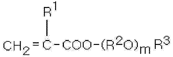 wobei R1 ein Wasserstoffatom oder Methyl ist;R2O ein C2-C4-Oxyalkylen oder ein Gemisch davon ist und statistisch oder in der Form eines Blocks zugegeben werden kann, für den Fall, dass dieses eine Kombination von zumindest zwei Arten C2-C4-Oxyalkylengruppen ist;R3 ein C1-C4 Alkyl ist; undm eine durchschnittliche Zugabemolzahl der Alkylengruppen ist und eine ganze Zahl von 1 bis 50 ist.
 - CMP-Aufschlämmung nach Anspruch 1, die eine Nichteinheitlichkeit innerhalb des Wafers (WIWNU) von weniger als 6,5% zeigt, wenn diese zum Polieren eines Wafers verwendet wird.
- CMP Aufschlämmung nach Anspruch 1, wobei die Verbindung mit einem Gewichtsmittel des Molekulargewichts von 30 bis 500 und enthaltend eine Hydroxylgruppe (OH), eine Carboxylgruppe (COOH) oder beide eine oder mehrere ist ausgewählt aus der Gruppe, bestehend aus Citrat-enthaltenden Verbindungen, Gluconat-enthaltenden Verbindungen, Malat-enthaltenden Verbindungen, Tatratenthaltenden Verbindungen, 2-Hydroxiisobutyrat-enthaltenden Verbindungen, Adipatenthaltenden Verbindungen, Octanoat-enthaltenden Verbindungen, Succinatenthaltenden Verbindungen, Ethylendiamintetraacetat-enthaltenden Verbindungen, Glutarat-enthaltenden Verbindungen, Methylensuccinat-enthaltenden Verbindungen, Mannose, Glycerogalactoheptose, Erythromannooctose, Arabinogalactononose und Glutamin.
- CMP-Aufschlämmung nach Anspruch 1, wobei die Verbindung mit einem Gewichtsmittel des Molekulargewichts von 30 bis 500 und enthaltend eine Hydroxylgruppe (OH), eine Carboxylgruppe (COOH) oder beide in einer Menge von 0,1 bis 30 Gewichtsteilen, bezogen auf 100 Gewichtsteile der abrasiven Partikel in der CMP-Aufschlämmung, enthalten ist.
- CMP-Aufschlämmung nach Anspruch 4, wobei das Additiv in einer Menge von 0,1 bis 10 Gewichtsteilen, bezogen auf 100 Gewichtsteile der CMP-Aufschlämmung, enthalten ist.
- CMP-Aufschlämmung nach Anspruch 1, wobei die abrasiven Partikel Ceroxidpartikel sind.
- CMP-Aufschlämmung nach Anspruch 1, wobei die abrasiven Partikel in einer Menge von 0,1 bis 10 Gewichtsteilen, bezogen auf 100 Gewichtsteile der CMP-Aufschlämmung, enthalten sind.
- Verfahren zum Polieren eines halbleitenden Wafers unter Verwendung der CMP-Aufschlämmung wie in einem der Ansprüche 1 bis 7 definiert.
- Verfahren nach Anspruch 8, wobei die Nichteinheitlichkeit innerhalb des Wafers (WIWNU) kontrolliert wird, um weniger als 6,5% zu sein.
Applications Claiming Priority (2)
| Application Number | Priority Date | Filing Date | Title |
|---|---|---|---|
| KR20060007995 | 2006-01-25 | ||
| PCT/KR2007/000332 WO2007086665A1 (en) | 2006-01-25 | 2007-01-19 | Cmp slurry and method for polishing semiconductor wafer using the same |
Publications (3)
| Publication Number | Publication Date |
|---|---|
| EP1994112A1 EP1994112A1 (de) | 2008-11-26 |
| EP1994112A4 EP1994112A4 (de) | 2010-12-08 |
| EP1994112B1 true EP1994112B1 (de) | 2018-09-19 |
Family
ID=38309412
Family Applications (1)
| Application Number | Title | Priority Date | Filing Date |
|---|---|---|---|
| EP07701029.6A Not-in-force EP1994112B1 (de) | 2006-01-25 | 2007-01-19 | Cmp-aufschlämmung und davon gebrauch machendes verfahren zum polieren von halbleiterscheiben |
Country Status (7)
| Country | Link |
|---|---|
| US (1) | US7736530B2 (de) |
| EP (1) | EP1994112B1 (de) |
| JP (1) | JP5290769B2 (de) |
| KR (1) | KR100880107B1 (de) |
| CN (1) | CN101374922B (de) |
| TW (1) | TWI313209B (de) |
| WO (1) | WO2007086665A1 (de) |
Families Citing this family (15)
| Publication number | Priority date | Publication date | Assignee | Title |
|---|---|---|---|---|
| KR101256551B1 (ko) | 2008-03-06 | 2013-04-19 | 주식회사 엘지화학 | Cmp 슬러리 및 이를 이용한 연마 방법 |
| US20110177623A1 (en) * | 2010-01-15 | 2011-07-21 | Confluense Llc | Active Tribology Management of CMP Polishing Material |
| KR101292328B1 (ko) * | 2010-02-04 | 2013-08-01 | 주식회사 엘지화학 | 균일한 입자크기 분포를 갖는 산화세륨 나노분말 및 그 제조방법 |
| WO2012032469A1 (en) | 2010-09-08 | 2012-03-15 | Basf Se | Aqueous polishing composition and process for chemically mechanically polishing substrate materials for electrical, mechanical and optical devices |
| JP2013540850A (ja) | 2010-09-08 | 2013-11-07 | ビーエーエスエフ ソシエタス・ヨーロピア | N−置換ジアゼニウムジオキシド及び/又はn’−ヒドロキシジアゼニウムオキシド塩を含有する水性研磨剤組成物 |
| WO2012032451A1 (en) | 2010-09-08 | 2012-03-15 | Basf Se | Aqueous polishing composition and process for chemically mechanically polishing substrates containing silicon oxide dielectric and polysilicon films |
| WO2012032467A1 (en) * | 2010-09-08 | 2012-03-15 | Basf Se | Process for chemically mechanically polishing substrates containing silicon oxide dielectric films and polysilicon and/or silicon nitride films |
| EP2649144A4 (de) | 2010-12-10 | 2014-05-14 | Basf Se | Wässrige polierzusammensetzung und verfahren zum chemisch-mechanischen polieren von substraten mit dielektrischen siliciumoxid- und polysiliciumfilmen |
| JP2012146975A (ja) * | 2010-12-24 | 2012-08-02 | Hitachi Chem Co Ltd | 研磨液及びこの研磨液を用いた基板の研磨方法 |
| EP2826827B1 (de) * | 2013-07-18 | 2019-06-12 | Basf Se | CMP-Zusammensetzung mit ceriahaltigen Schleifteilchen |
| TWI626117B (zh) * | 2017-01-19 | 2018-06-11 | 智勝科技股份有限公司 | 研磨墊及研磨方法 |
| US10037889B1 (en) * | 2017-03-29 | 2018-07-31 | Rohm And Haas Electronic Materials Cmp Holdings, Inc. | Cationic particle containing slurries and methods of using them for CMP of spin-on carbon films |
| CN109096924B (zh) * | 2018-09-17 | 2021-07-30 | 宁波日晟新材料有限公司 | 一种玻璃自由曲面表面抛光液及其制备方法和应用 |
| US20200095502A1 (en) | 2018-09-26 | 2020-03-26 | Versum Materials Us, Llc | High Oxide VS Nitride Selectivity, Low And Uniform Oxide Trench Dishing In Shallow Trench Isolation(STI) Chemical Mechanical Planarization Polishing(CMP) |
| TW202547985A (zh) * | 2024-03-25 | 2025-12-16 | 美商恩特葛瑞斯股份有限公司 | 氧化鈰及異羥肟酸化學機械拋光(cmp)組合物 |
Family Cites Families (41)
| Publication number | Priority date | Publication date | Assignee | Title |
|---|---|---|---|---|
| JP3278532B2 (ja) * | 1994-07-08 | 2002-04-30 | 株式会社東芝 | 半導体装置の製造方法 |
| WO1997029510A1 (fr) | 1996-02-07 | 1997-08-14 | Hitachi Chemical Company, Ltd. | Abrasif d'oxyde de cerium, microplaquette semi-conductrice, dispositif semi-conducteur, procede pour les produire et procede pour polir les substrats |
| JPH1027041A (ja) | 1996-07-12 | 1998-01-27 | Hitachi Ltd | リセット機能付き制御装置 |
| JPH10154672A (ja) | 1996-09-30 | 1998-06-09 | Hitachi Chem Co Ltd | 酸化セリウム研磨剤及び基板の研磨法 |
| JPH10106988A (ja) | 1996-09-30 | 1998-04-24 | Hitachi Chem Co Ltd | 酸化セリウム研磨剤及び基板の研磨法 |
| EP0853335A3 (de) | 1997-01-10 | 1999-01-07 | Texas Instruments Incorporated | Suspension und Verfahren zum mechnisch-chemischen Polieren von Halbleiteranordnungen |
| ES2216490T3 (es) * | 1998-02-24 | 2004-10-16 | Showa Denko Kabushiki Kaisha | Composicion abrasiva para pulir un dispositivo semiconductor y procedimiento para producir un dispositivo semiconductor con la misma. |
| TW455626B (en) * | 1998-07-23 | 2001-09-21 | Eternal Chemical Co Ltd | Chemical mechanical abrasive composition for use in semiconductor processing |
| JP2000063216A (ja) * | 1998-08-12 | 2000-02-29 | Sumitomo Chem Co Ltd | 除草剤組成物 |
| JP2000109794A (ja) | 1998-10-08 | 2000-04-18 | Hitachi Chem Co Ltd | Cmp研磨剤及び基板の研磨方法 |
| JP2000109815A (ja) | 1998-10-08 | 2000-04-18 | Hitachi Chem Co Ltd | Cmp研磨剤及び基板の研磨方法 |
| KR100754103B1 (ko) | 1998-12-25 | 2007-08-31 | 히다치 가세고교 가부시끼가이샤 | Cmp 연마제, cmp 연마제용 첨가액 및 기판의 연마방법 |
| WO2000079577A1 (en) | 1999-06-18 | 2000-12-28 | Hitachi Chemical Co., Ltd. | Abrasive compound for cmp, method for polishing substrate and method for manufacturing semiconductor device using the same, and additive for cmp abrasive compound |
| JP4555936B2 (ja) | 1999-07-21 | 2010-10-06 | 日立化成工業株式会社 | Cmp研磨液 |
| JP4386500B2 (ja) | 1999-07-27 | 2009-12-16 | シチズン狭山株式会社 | 円板状体搬送装置 |
| KR20010046395A (ko) * | 1999-11-12 | 2001-06-15 | 안복현 | 연마용 조성물 |
| TWI296006B (de) | 2000-02-09 | 2008-04-21 | Jsr Corp | |
| JP3997053B2 (ja) * | 2000-04-28 | 2007-10-24 | 花王株式会社 | ロールオフ低減剤 |
| JP2001319900A (ja) | 2000-05-10 | 2001-11-16 | Toshiba Ceramics Co Ltd | 半導体基板の研磨方法 |
| JP2004506337A (ja) | 2000-08-11 | 2004-02-26 | ロデール ホールディングス インコーポレイテッド | 金属基板の化学機械平坦化 |
| KR100464429B1 (ko) * | 2002-08-16 | 2005-01-03 | 삼성전자주식회사 | 화학 기계적 폴리싱 슬러리 및 이를 사용한 화학 기계적폴리싱 방법 |
| KR100475457B1 (ko) | 2001-11-15 | 2005-03-08 | 삼성전자주식회사 | 슬러리용 첨가제 조성물, 이를 포함하는 슬러리 조성물 및연마 방법 |
| US6821897B2 (en) * | 2001-12-05 | 2004-11-23 | Cabot Microelectronics Corporation | Method for copper CMP using polymeric complexing agents |
| US6776810B1 (en) * | 2002-02-11 | 2004-08-17 | Cabot Microelectronics Corporation | Anionic abrasive particles treated with positively charged polyelectrolytes for CMP |
| US7677956B2 (en) | 2002-05-10 | 2010-03-16 | Cabot Microelectronics Corporation | Compositions and methods for dielectric CMP |
| KR100497608B1 (ko) | 2002-08-05 | 2005-07-01 | 삼성전자주식회사 | 슬러리 조성물 및 이의 제조 방법과 이를 사용한 연마 방법 |
| JP3875156B2 (ja) * | 2002-08-07 | 2007-01-31 | 花王株式会社 | ロールオフ低減剤 |
| JP4446371B2 (ja) * | 2002-08-30 | 2010-04-07 | 花王株式会社 | 研磨液組成物 |
| KR100494117B1 (ko) | 2002-12-26 | 2005-06-13 | 매그나칩 반도체 유한회사 | 반도체 소자의 얕은 트랜치 소자분리막 형성방법 |
| US20040216388A1 (en) * | 2003-03-17 | 2004-11-04 | Sharad Mathur | Slurry compositions for use in a chemical-mechanical planarization process |
| KR100577348B1 (ko) | 2003-05-06 | 2006-05-08 | 한화석유화학 주식회사 | 얕은 트렌치 소자 분리용 화학적 기계적 연마 슬러리 |
| US7736405B2 (en) * | 2003-05-12 | 2010-06-15 | Advanced Technology Materials, Inc. | Chemical mechanical polishing compositions for copper and associated materials and method of using same |
| KR100539983B1 (ko) | 2003-05-15 | 2006-01-10 | 학교법인 한양학원 | Cmp용 세리아 연마제 및 그 제조 방법 |
| JP4637464B2 (ja) * | 2003-07-01 | 2011-02-23 | Jsr株式会社 | 化学機械研磨用水系分散体 |
| KR101053653B1 (ko) * | 2003-07-01 | 2011-08-02 | 주식회사 동진쎄미켐 | 산화세륨 연마제를 이용한 화학 기계적 연마 슬러리조성물 |
| US20050108947A1 (en) * | 2003-11-26 | 2005-05-26 | Mueller Brian L. | Compositions and methods for chemical mechanical polishing silica and silicon nitride |
| EP1566420A1 (de) * | 2004-01-23 | 2005-08-24 | JSR Corporation | Wässrige Dispersionsaufschlämmung für chemisch/mechanische Polierung und Verwendung in einem Polierverfahren |
| KR100588404B1 (ko) * | 2004-03-16 | 2006-06-12 | 삼성코닝 주식회사 | 반도체 박막 연마용 산화세륨 슬러리 |
| KR101050348B1 (ko) | 2004-05-31 | 2011-07-19 | 엘지디스플레이 주식회사 | 횡전계 액정표시장치 |
| JP2006019740A (ja) * | 2004-06-30 | 2006-01-19 | Dongjin Semichem Co Ltd | 化学的機械的研磨スラリー組成物 |
| EP1844122B1 (de) * | 2004-12-29 | 2013-02-20 | LG Chem, Ltd. | Zusatzstoff zu cmp-aufschlämmung |
-
2007
- 2007-01-19 CN CN2007800033319A patent/CN101374922B/zh not_active Expired - Fee Related
- 2007-01-19 KR KR1020070006040A patent/KR100880107B1/ko not_active Expired - Fee Related
- 2007-01-19 JP JP2008551192A patent/JP5290769B2/ja not_active Expired - Fee Related
- 2007-01-19 WO PCT/KR2007/000332 patent/WO2007086665A1/en not_active Ceased
- 2007-01-19 EP EP07701029.6A patent/EP1994112B1/de not_active Not-in-force
- 2007-01-24 US US11/657,051 patent/US7736530B2/en active Active
- 2007-01-25 TW TW096102785A patent/TWI313209B/zh not_active IP Right Cessation
Also Published As
| Publication number | Publication date |
|---|---|
| TW200800486A (en) | 2008-01-01 |
| WO2007086665A1 (en) | 2007-08-02 |
| KR20070078064A (ko) | 2007-07-30 |
| KR100880107B1 (ko) | 2009-01-21 |
| WO2007086665A9 (en) | 2011-11-24 |
| US7736530B2 (en) | 2010-06-15 |
| JP2009524236A (ja) | 2009-06-25 |
| CN101374922A (zh) | 2009-02-25 |
| EP1994112A1 (de) | 2008-11-26 |
| TWI313209B (en) | 2009-08-11 |
| EP1994112A4 (de) | 2010-12-08 |
| CN101374922B (zh) | 2013-06-12 |
| JP5290769B2 (ja) | 2013-09-18 |
| US20070191244A1 (en) | 2007-08-16 |
Similar Documents
| Publication | Publication Date | Title |
|---|---|---|
| US7736530B2 (en) | CMP slurry and method for polishing semiconductor wafer using the same | |
| EP1279708B1 (de) | Schleifmittelzusammensetzung und Polierverfahren unter Verwendung derselben | |
| EP1962334A1 (de) | Wässrige dispersion zum chemisch-mechanischen polieren, verfahren zum chemisch-mechanischen polieren und kit zum herstellen einer wässrigen dispersion zum chemisch-mechanischen polieren | |
| EP2825609A1 (de) | Oxid- und nitridselektive cmp-zusammensetzungen mit hoher beseitigungsrate und geringer empfindlichkeit | |
| CN101767295A (zh) | 化学机械抛光组合物及其相关方法 | |
| US8652967B2 (en) | Adjuvant for controlling polishing selectivity and chemical mechanical polishing slurry comprising the same | |
| KR100674927B1 (ko) | Cmp용 슬러리 조성물 및 그 제조 방법과 이들을 이용한기판 연마 방법 | |
| KR101718798B1 (ko) | 안정화된 화학 기계적 연마 조성물 및 기판의 연마 방법 | |
| EP1957600B1 (de) | Hilfsstoff zur gezielten einstellung der polierselektivität sowie ihn enthaltendes cmp-poliermittel | |
| US20060207188A1 (en) | Ceria abrasive for cmp | |
| EP1844122B1 (de) | Zusatzstoff zu cmp-aufschlämmung | |
| KR102656513B1 (ko) | Cmp 슬러리 조성물 | |
| TW202344640A (zh) | 用於矽氧化物、矽氮化物及多晶矽的選擇性及非選擇性cmp之基於氧化鈰的漿料組合物 |
Legal Events
| Date | Code | Title | Description |
|---|---|---|---|
| PUAI | Public reference made under article 153(3) epc to a published international application that has entered the european phase |
Free format text: ORIGINAL CODE: 0009012 |
|
| 17P | Request for examination filed |
Effective date: 20080731 |
|
| AK | Designated contracting states |
Kind code of ref document: A1 Designated state(s): AT BE BG CH CY CZ DE DK EE ES FI FR GB GR HU IE IS IT LI LT LU LV MC NL PL PT RO SE SI SK TR |
|
| RIN1 | Information on inventor provided before grant (corrected) |
Inventor name: CHO, SEUNG-BEOM Inventor name: KIM, JONG-PIL Inventor name: KIM, JANG-YUL Inventor name: NHO, JUN-SEOK Inventor name: OH, MYOUNG-HWAN |
|
| A4 | Supplementary search report drawn up and despatched |
Effective date: 20101105 |
|
| RIC1 | Information provided on ipc code assigned before grant |
Ipc: C09G 1/02 20060101AFI20101029BHEP Ipc: H01L 21/321 20060101ALI20101029BHEP |
|
| DAX | Request for extension of the european patent (deleted) | ||
| 17Q | First examination report despatched |
Effective date: 20151116 |
|
| STAA | Information on the status of an ep patent application or granted ep patent |
Free format text: STATUS: EXAMINATION IS IN PROGRESS |
|
| GRAP | Despatch of communication of intention to grant a patent |
Free format text: ORIGINAL CODE: EPIDOSNIGR1 |
|
| STAA | Information on the status of an ep patent application or granted ep patent |
Free format text: STATUS: GRANT OF PATENT IS INTENDED |
|
| INTG | Intention to grant announced |
Effective date: 20180622 |
|
| GRAS | Grant fee paid |
Free format text: ORIGINAL CODE: EPIDOSNIGR3 |
|
| GRAA | (expected) grant |
Free format text: ORIGINAL CODE: 0009210 |
|
| STAA | Information on the status of an ep patent application or granted ep patent |
Free format text: STATUS: THE PATENT HAS BEEN GRANTED |
|
| AK | Designated contracting states |
Kind code of ref document: B1 Designated state(s): AT BE BG CH CY CZ DE DK EE ES FI FR GB GR HU IE IS IT LI LT LU LV MC NL PL PT RO SE SI SK TR |
|
| RAP1 | Party data changed (applicant data changed or rights of an application transferred) |
Owner name: LG CHEM, LTD. |
|
| REG | Reference to a national code |
Ref country code: GB Ref legal event code: FG4D |
|
| REG | Reference to a national code |
Ref country code: CH Ref legal event code: EP |
|
| REG | Reference to a national code |
Ref country code: AT Ref legal event code: REF Ref document number: 1043227 Country of ref document: AT Kind code of ref document: T Effective date: 20181015 |
|
| REG | Reference to a national code |
Ref country code: IE Ref legal event code: FG4D |
|
| REG | Reference to a national code |
Ref country code: DE Ref legal event code: R096 Ref document number: 602007056179 Country of ref document: DE |
|
| REG | Reference to a national code |
Ref country code: NL Ref legal event code: MP Effective date: 20180919 |
|
| PG25 | Lapsed in a contracting state [announced via postgrant information from national office to epo] |
Ref country code: BG Free format text: LAPSE BECAUSE OF FAILURE TO SUBMIT A TRANSLATION OF THE DESCRIPTION OR TO PAY THE FEE WITHIN THE PRESCRIBED TIME-LIMIT Effective date: 20181219 Ref country code: SE Free format text: LAPSE BECAUSE OF FAILURE TO SUBMIT A TRANSLATION OF THE DESCRIPTION OR TO PAY THE FEE WITHIN THE PRESCRIBED TIME-LIMIT Effective date: 20180919 Ref country code: LT Free format text: LAPSE BECAUSE OF FAILURE TO SUBMIT A TRANSLATION OF THE DESCRIPTION OR TO PAY THE FEE WITHIN THE PRESCRIBED TIME-LIMIT Effective date: 20180919 Ref country code: FI Free format text: LAPSE BECAUSE OF FAILURE TO SUBMIT A TRANSLATION OF THE DESCRIPTION OR TO PAY THE FEE WITHIN THE PRESCRIBED TIME-LIMIT Effective date: 20180919 Ref country code: GR Free format text: LAPSE BECAUSE OF FAILURE TO SUBMIT A TRANSLATION OF THE DESCRIPTION OR TO PAY THE FEE WITHIN THE PRESCRIBED TIME-LIMIT Effective date: 20181220 |
|
| REG | Reference to a national code |
Ref country code: LT Ref legal event code: MG4D |
|
| PG25 | Lapsed in a contracting state [announced via postgrant information from national office to epo] |
Ref country code: LV Free format text: LAPSE BECAUSE OF FAILURE TO SUBMIT A TRANSLATION OF THE DESCRIPTION OR TO PAY THE FEE WITHIN THE PRESCRIBED TIME-LIMIT Effective date: 20180919 |
|
| REG | Reference to a national code |
Ref country code: AT Ref legal event code: MK05 Ref document number: 1043227 Country of ref document: AT Kind code of ref document: T Effective date: 20180919 |
|
| PG25 | Lapsed in a contracting state [announced via postgrant information from national office to epo] |
Ref country code: RO Free format text: LAPSE BECAUSE OF FAILURE TO SUBMIT A TRANSLATION OF THE DESCRIPTION OR TO PAY THE FEE WITHIN THE PRESCRIBED TIME-LIMIT Effective date: 20180919 Ref country code: CZ Free format text: LAPSE BECAUSE OF FAILURE TO SUBMIT A TRANSLATION OF THE DESCRIPTION OR TO PAY THE FEE WITHIN THE PRESCRIBED TIME-LIMIT Effective date: 20180919 Ref country code: NL Free format text: LAPSE BECAUSE OF FAILURE TO SUBMIT A TRANSLATION OF THE DESCRIPTION OR TO PAY THE FEE WITHIN THE PRESCRIBED TIME-LIMIT Effective date: 20180919 Ref country code: IT Free format text: LAPSE BECAUSE OF FAILURE TO SUBMIT A TRANSLATION OF THE DESCRIPTION OR TO PAY THE FEE WITHIN THE PRESCRIBED TIME-LIMIT Effective date: 20180919 Ref country code: AT Free format text: LAPSE BECAUSE OF FAILURE TO SUBMIT A TRANSLATION OF THE DESCRIPTION OR TO PAY THE FEE WITHIN THE PRESCRIBED TIME-LIMIT Effective date: 20180919 Ref country code: EE Free format text: LAPSE BECAUSE OF FAILURE TO SUBMIT A TRANSLATION OF THE DESCRIPTION OR TO PAY THE FEE WITHIN THE PRESCRIBED TIME-LIMIT Effective date: 20180919 Ref country code: ES Free format text: LAPSE BECAUSE OF FAILURE TO SUBMIT A TRANSLATION OF THE DESCRIPTION OR TO PAY THE FEE WITHIN THE PRESCRIBED TIME-LIMIT Effective date: 20180919 Ref country code: PL Free format text: LAPSE BECAUSE OF FAILURE TO SUBMIT A TRANSLATION OF THE DESCRIPTION OR TO PAY THE FEE WITHIN THE PRESCRIBED TIME-LIMIT Effective date: 20180919 Ref country code: IS Free format text: LAPSE BECAUSE OF FAILURE TO SUBMIT A TRANSLATION OF THE DESCRIPTION OR TO PAY THE FEE WITHIN THE PRESCRIBED TIME-LIMIT Effective date: 20190119 |
|
| PG25 | Lapsed in a contracting state [announced via postgrant information from national office to epo] |
Ref country code: SK Free format text: LAPSE BECAUSE OF FAILURE TO SUBMIT A TRANSLATION OF THE DESCRIPTION OR TO PAY THE FEE WITHIN THE PRESCRIBED TIME-LIMIT Effective date: 20180919 Ref country code: PT Free format text: LAPSE BECAUSE OF FAILURE TO SUBMIT A TRANSLATION OF THE DESCRIPTION OR TO PAY THE FEE WITHIN THE PRESCRIBED TIME-LIMIT Effective date: 20190119 |
|
| REG | Reference to a national code |
Ref country code: DE Ref legal event code: R097 Ref document number: 602007056179 Country of ref document: DE |
|
| PLBE | No opposition filed within time limit |
Free format text: ORIGINAL CODE: 0009261 |
|
| STAA | Information on the status of an ep patent application or granted ep patent |
Free format text: STATUS: NO OPPOSITION FILED WITHIN TIME LIMIT |
|
| PG25 | Lapsed in a contracting state [announced via postgrant information from national office to epo] |
Ref country code: DK Free format text: LAPSE BECAUSE OF FAILURE TO SUBMIT A TRANSLATION OF THE DESCRIPTION OR TO PAY THE FEE WITHIN THE PRESCRIBED TIME-LIMIT Effective date: 20180919 |
|
| 26N | No opposition filed |
Effective date: 20190620 |
|
| PG25 | Lapsed in a contracting state [announced via postgrant information from national office to epo] |
Ref country code: MC Free format text: LAPSE BECAUSE OF FAILURE TO SUBMIT A TRANSLATION OF THE DESCRIPTION OR TO PAY THE FEE WITHIN THE PRESCRIBED TIME-LIMIT Effective date: 20180919 |
|
| REG | Reference to a national code |
Ref country code: CH Ref legal event code: PL |
|
| PG25 | Lapsed in a contracting state [announced via postgrant information from national office to epo] |
Ref country code: LU Free format text: LAPSE BECAUSE OF NON-PAYMENT OF DUE FEES Effective date: 20190119 |
|
| REG | Reference to a national code |
Ref country code: BE Ref legal event code: MM Effective date: 20190131 |
|
| REG | Reference to a national code |
Ref country code: IE Ref legal event code: MM4A |
|
| PG25 | Lapsed in a contracting state [announced via postgrant information from national office to epo] |
Ref country code: SI Free format text: LAPSE BECAUSE OF FAILURE TO SUBMIT A TRANSLATION OF THE DESCRIPTION OR TO PAY THE FEE WITHIN THE PRESCRIBED TIME-LIMIT Effective date: 20180919 |
|
| PG25 | Lapsed in a contracting state [announced via postgrant information from national office to epo] |
Ref country code: BE Free format text: LAPSE BECAUSE OF NON-PAYMENT OF DUE FEES Effective date: 20190131 |
|
| PG25 | Lapsed in a contracting state [announced via postgrant information from national office to epo] |
Ref country code: LI Free format text: LAPSE BECAUSE OF NON-PAYMENT OF DUE FEES Effective date: 20190131 Ref country code: CH Free format text: LAPSE BECAUSE OF NON-PAYMENT OF DUE FEES Effective date: 20190131 |
|
| PG25 | Lapsed in a contracting state [announced via postgrant information from national office to epo] |
Ref country code: IE Free format text: LAPSE BECAUSE OF NON-PAYMENT OF DUE FEES Effective date: 20190119 |
|
| PG25 | Lapsed in a contracting state [announced via postgrant information from national office to epo] |
Ref country code: TR Free format text: LAPSE BECAUSE OF FAILURE TO SUBMIT A TRANSLATION OF THE DESCRIPTION OR TO PAY THE FEE WITHIN THE PRESCRIBED TIME-LIMIT Effective date: 20180919 |
|
| PG25 | Lapsed in a contracting state [announced via postgrant information from national office to epo] |
Ref country code: CY Free format text: LAPSE BECAUSE OF FAILURE TO SUBMIT A TRANSLATION OF THE DESCRIPTION OR TO PAY THE FEE WITHIN THE PRESCRIBED TIME-LIMIT Effective date: 20180919 |
|
| PG25 | Lapsed in a contracting state [announced via postgrant information from national office to epo] |
Ref country code: HU Free format text: LAPSE BECAUSE OF FAILURE TO SUBMIT A TRANSLATION OF THE DESCRIPTION OR TO PAY THE FEE WITHIN THE PRESCRIBED TIME-LIMIT; INVALID AB INITIO Effective date: 20070119 |
|
| PGFP | Annual fee paid to national office [announced via postgrant information from national office to epo] |
Ref country code: GB Payment date: 20221220 Year of fee payment: 17 Ref country code: FR Payment date: 20221220 Year of fee payment: 17 |
|
| PGFP | Annual fee paid to national office [announced via postgrant information from national office to epo] |
Ref country code: DE Payment date: 20221220 Year of fee payment: 17 |
|
| REG | Reference to a national code |
Ref country code: DE Ref legal event code: R119 Ref document number: 602007056179 Country of ref document: DE |
|
| GBPC | Gb: european patent ceased through non-payment of renewal fee |
Effective date: 20240119 |
|
| PG25 | Lapsed in a contracting state [announced via postgrant information from national office to epo] |
Ref country code: DE Free format text: LAPSE BECAUSE OF NON-PAYMENT OF DUE FEES Effective date: 20240801 |
|
| PG25 | Lapsed in a contracting state [announced via postgrant information from national office to epo] |
Ref country code: GB Free format text: LAPSE BECAUSE OF NON-PAYMENT OF DUE FEES Effective date: 20240119 |
|
| PG25 | Lapsed in a contracting state [announced via postgrant information from national office to epo] |
Ref country code: FR Free format text: LAPSE BECAUSE OF NON-PAYMENT OF DUE FEES Effective date: 20240131 |
|
| PG25 | Lapsed in a contracting state [announced via postgrant information from national office to epo] |
Ref country code: GB Free format text: LAPSE BECAUSE OF NON-PAYMENT OF DUE FEES Effective date: 20240119 Ref country code: FR Free format text: LAPSE BECAUSE OF NON-PAYMENT OF DUE FEES Effective date: 20240131 Ref country code: DE Free format text: LAPSE BECAUSE OF NON-PAYMENT OF DUE FEES Effective date: 20240801 |