EP1995663A1 - System und Verfahren zur lokalen Erzeugung von Programmdaten in einer programmierbaren Vorrichtung - Google Patents
System und Verfahren zur lokalen Erzeugung von Programmdaten in einer programmierbaren Vorrichtung Download PDFInfo
- Publication number
- EP1995663A1 EP1995663A1 EP07108690A EP07108690A EP1995663A1 EP 1995663 A1 EP1995663 A1 EP 1995663A1 EP 07108690 A EP07108690 A EP 07108690A EP 07108690 A EP07108690 A EP 07108690A EP 1995663 A1 EP1995663 A1 EP 1995663A1
- Authority
- EP
- European Patent Office
- Prior art keywords
- programming data
- data
- programmable logic
- programming
- bypass
- Prior art date
- Legal status (The legal status is an assumption and is not a legal conclusion. Google has not performed a legal analysis and makes no representation as to the accuracy of the status listed.)
- Withdrawn
Links
Images


Classifications
-
- G—PHYSICS
- G06—COMPUTING OR CALCULATING; COUNTING
- G06F—ELECTRIC DIGITAL DATA PROCESSING
- G06F30/00—Computer-aided design [CAD]
- G06F30/30—Circuit design
- G06F30/34—Circuit design for reconfigurable circuits, e.g. field programmable gate arrays [FPGA] or programmable logic devices [PLD]
Definitions
- the present invention relates to a system and method for the local generation of programming data in a programmable logic device.
- methods of providing fault-tolerance in programmable logic devices comprise the steps of determining the required functional circuit size and adding an extra section, the redundant part being used to replace any defective parts after manufacture.
- fault-tolerance adds to the size and cost of each device, the number of devices which can be used (the yield) is increased to an extent which sees an overall reduction in the average cost of each usable device.
- Some fault-tolerant systems have a programming interface for each repeated region of the programmable device. Information about the location of the fault is used to redirect programming data from a faulty region to another.
- these solutions require extra dedicated circuitry to redirect the programming data. This additional routing circuitry further increases the size and cost of the programmable device, driving up the cost of each usable device.
- CAD Computer Aided Design
- an original program is altered in order to create a series of different programs, each one of which is design to avoid at least one area of the programmable logic device. Once a device is manufactured, it is tested to determine the presence and location of any fault. Based on the results of these tests, one of the altered programs is then chosen to program the device. Accordingly, it is possible to avoid the use of almost any faulty area of the device.
- this method not only requires the pre-programming of several altered programs, it also necessitates a complex manufacturing infrastructure in order to support the making of this kind of choice during the manufacturing process.
- the present invention provides a method of programming a programmable logic device, the programmable logic device comprising a plurality of serially connected programmable logic regions, the method comprises the steps of:
- the step of generating the effective programming data further comprises the steps of:
- the step of inserting the bypass programming data into the initial programming data may further comprise the steps of:
- the step of inserting the bypass programming data into the initial programming data may further comprise the steps of:
- the present invention further provide an apparatus for programming a programmable logic device, the programmable logic device comprising a plurality of serially connected programmable logic regions, the apparatus comprises:
- the effective programming data generating means further comprises:
- the inserting means may further comprise:
- the inserting means may further comprise:
- the present invention provides several advantages. For example, the present invention diminishes the programming and hardware overhead associated with fault-tolerance, thereby diminishing manufacturing cost and complexity. Also, the present invention provides a system and method of programming a programmable logic device which hides the existence of fault-tolerance from the CAD software generating the initial programming data. Moreover, the fault-tolerance provided by the method and system of the present invention is also hidden from the user, thus improving ease of use.
- a typical programmable logic device is programmed with a bitmap of data stored in memory distributed throughout the device. For each programmable element of the device, there is associated data stored in specific memory elements.
- the program memory in most programmable devices is populated with data in such a way as to enable the entire programmable device acts as one large memory (i.e. each element has an address that uniquely identifies it amongst all elements).
- an address and some data are presented to the device's programming interface. The programming interface then sends the data to the addressed element while all other elements remain inactive.
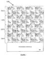
- FIG. 1 shows an example of such an architecture.
- the programmable logic device 100 of Figure 1 comprises a series of strips 101, 102, 103 and 104. Each strip 101, 102, 103 and 104 can be linked together. Accordingly, strips can be stacked in order to build larger coherent arrays.
- Each strip has a series of available routing resources which serve to connect the strips to each other.
- the available routing resources of a strip surrounded by two other strips can be programmed to a bypass mode by passing the connections input from a first adjacent strip to those output to a second adjacent strip, thereby rendering the middle strip logically invisible.
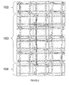
- Figure 2 shows a more detailed view of the routing resource of Figure 1 .
- the routing is shown as implemented using multiplexers. However, other implementations such as pass-gates or transmission-gates are possible.
- the routing network is repeated such that there are direct paths between the inputs and outputs of each strip. For example, the dotted line in Figure 2 shows how one input of strip 103 can be directly connected to the output of strip 103. Thus, the output of strip 102 can effectively be directly connected to the input of strip 104.
- programmable logic devices having an architecture based on repeated strips of logic blocks
- the user programmable logic device 100 comprises four strips (or regions) 101, 102, 103 and 104.
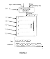
- three programming blocks A, B and C are to be programmed into the programmable logic device 100.
- First the programming data for the programmable device is created using Computer Aided Design (CAD) software.
- CAD Computer Aided Design
- the CAD software behaves as if it was programming a device containing only three regions and so generates data for only three regions.
- This programming data is then stored in order to subsequently be sent to the programming interface circuit 105.
- the results of tests carried out on the device are encoded and stored in memory so that they can also be sent to the programming interface circuit 105 at the time of programming.
- This information is contained in the input transformation data referred to in Figure 3 .
- region 103 is found to be faulty. Accordingly, the programming block C for that region will need to be moved to region 104. Moreover, the strip containing the faulty element must be programmed with a bypass configuration.
- the programming interface circuit 105 receives both programming data and transformation data.
- the programming interface circuit 105 then automatically alters the programming data in response to information about the location of the fault in the programmable device.
- the information relating to the location of the fault is contained in the transformation data.
- the actual bypass configuration may be relatively simple to generate. If this is the case, the programming interface circuit 105 will be relatively small. For example, if the required configuration merely requires the generation of a plurality of zeros, then the programming interface circuit 105 could merely comprise a counter and a multiplexer which would insert zeroes into the programming data for the correct number of configuration cycles.
- blocks A, B and C are to be programmed into a programmable logic device.
- the programming data for the programmable device is created using Computer Aided Design (CAD) software.
- CAD Computer Aided Design
- the CAD software behaves as if it was programming a device containing only three regions and so generates data for only three regions. This programming data is then stored in order to subsequently be sent to the programming interface circuit 110.
- the results of tests carried out on the device are encoded and stored in memory so that they can also be sent to the programming interface circuit 110 at the time of programming.
- regions 112 and 114 are found to be faulty. Accordingly, programming block B for which was originally meant for region 112 will need to be moved to region 113 and programming block C which was originally meant for region 113 will need to be moved to region 115.
- the each strip containing faulty elements must be programmed with a bypass configuration.
- the programming interface circuit 110 receives both programming data and transformation data.
- the programming interface circuit 110 then automatically alters the programming data in response to information about the location of the faults in the programmable device.
- the information relating to the locations of the faults is contained in the transformation data.
- the generation of the default configuration data can be performed as in the example of Figure 3 .
- the programming interface circuit 10-5, 110 of the present invention will assign the last regions as faulty in the transformation data. Accordingly, the first blocks in the device will be programmed with the programming data and the last blocks will be logically invisible.
- the circuit 105 receives the programming data and the transformation data.
- the circuit 105 must send default programming data to the programmable logic device at the appropriate time in order to create the effective programming data.
- the programming interface 105 comprises a Finite State Machine (FSM) 106 which monitors control signals coming from the external interface and the programmable device 100.
- the FSM 106 determines the appropriate time for inserting default programming data and controls the data insertion operation.
- the FSM 106 also generates output control signals to the external and programmable device interfaces.
- FSM Finite State Machine
- One method which could be used by the FSM 106 to determine when to insert the default programming data would be count the number of configuration data elements which have been sent to the array. If it takes Y data elements to configure each strip and the Nth strip is defective, the default programming data should be inserted after YxN data elements have been transferred. As will be appreciated by the skilled reader, other methods of determining when to insert default configuration data are also possible. For example, there may be special code words or tags in the programming data which identify when the programming of a strip is complete. In this case, the FSM 106 could be programmed to recognise and count the code words to determine when to insert the default programming data.
- the FSM 106 determines that it is the appropriate time to insert the default programming data, it switches the output of multiplexer 108 between the input programming data and the internally generated default programming data generated by the default programming data generator 107. Once the default programming data is sent, the output of multiplexer 108 is switched back to the input programming data and the subsequent regions are programmed.
- the result of the above operations is that, although the programming data which was input into the programming interface contains information to program regions 101, 102 and 103, the effective programming data contains enough information to program four regions 101, 102, 103 and 104.
- the operation and implementation of the programming interface may be varied. For example, if the programming data is sent from a local cache memory, then the programming interface will pause reading the memory (i.e. using the control signal shown in Figure 3 ) while it generates the data. Alternatively, if the programming data is being sent by some other entity in the system and cannot be stopped, then the programming interface circuit 105 may comprise a First-In-First-Out buffer (not shown) within which it will store the incoming programming data while inserting generated data into the effective programming data.
Landscapes
- Engineering & Computer Science (AREA)
- Computer Hardware Design (AREA)
- Physics & Mathematics (AREA)
- Theoretical Computer Science (AREA)
- Evolutionary Computation (AREA)
- Geometry (AREA)
- General Engineering & Computer Science (AREA)
- General Physics & Mathematics (AREA)
- Logic Circuits (AREA)
Priority Applications (3)
| Application Number | Priority Date | Filing Date | Title |
|---|---|---|---|
| EP07108690A EP1995663A1 (de) | 2007-05-22 | 2007-05-22 | System und Verfahren zur lokalen Erzeugung von Programmdaten in einer programmierbaren Vorrichtung |
| US12/123,670 US7679400B2 (en) | 2007-05-22 | 2008-05-20 | System and method for local generation of programming data in a programmable device |
| JP2008133342A JP2008295046A (ja) | 2007-05-22 | 2008-05-21 | プログラマブルデバイス内のプログラミングデータをローカルに生成するシステムおよび方法 |
Applications Claiming Priority (1)
| Application Number | Priority Date | Filing Date | Title |
|---|---|---|---|
| EP07108690A EP1995663A1 (de) | 2007-05-22 | 2007-05-22 | System und Verfahren zur lokalen Erzeugung von Programmdaten in einer programmierbaren Vorrichtung |
Publications (1)
| Publication Number | Publication Date |
|---|---|
| EP1995663A1 true EP1995663A1 (de) | 2008-11-26 |
Family
ID=38740336
Family Applications (1)
| Application Number | Title | Priority Date | Filing Date |
|---|---|---|---|
| EP07108690A Withdrawn EP1995663A1 (de) | 2007-05-22 | 2007-05-22 | System und Verfahren zur lokalen Erzeugung von Programmdaten in einer programmierbaren Vorrichtung |
Country Status (3)
| Country | Link |
|---|---|
| US (1) | US7679400B2 (de) |
| EP (1) | EP1995663A1 (de) |
| JP (1) | JP2008295046A (de) |
Citations (3)
| Publication number | Priority date | Publication date | Assignee | Title |
|---|---|---|---|---|
| EP0351983A2 (de) | 1988-07-22 | 1990-01-24 | Altera Corporation | Geräte mit programmierbarer Logik mit Ersatzschaltungen zum Ersetzen defekter Schaltungen |
| WO2002027928A2 (en) | 2000-09-28 | 2002-04-04 | Xilinx, Inc. | Method and apparatus for tolerating defects in a programmable logic device using runtime parameterizable cores |
| US6874108B1 (en) | 2001-08-27 | 2005-03-29 | Agere Systems Inc. | Fault tolerant operation of reconfigurable devices utilizing an adjustable system clock |
Family Cites Families (10)
| Publication number | Priority date | Publication date | Assignee | Title |
|---|---|---|---|---|
| JP2909328B2 (ja) * | 1992-11-02 | 1999-06-23 | 株式会社東芝 | フィールドプログラマブルゲートアレイ |
| JP2001223611A (ja) * | 2000-02-10 | 2001-08-17 | Matsushita Electric Ind Co Ltd | 受信装置 |
| EP1162747B1 (de) * | 2000-04-26 | 2012-02-29 | Altera Corporation | Leitungssegmentierung in programmierbaren logischen Vorrichtungen mit redundanten Schaltungen |
| US6965249B2 (en) * | 2001-10-15 | 2005-11-15 | Altera Corporation | Programmable logic device with redundant circuitry |
| US7145344B2 (en) * | 2002-10-25 | 2006-12-05 | Xilinx, Inc. | Method and circuits for localizing defective interconnect resources in programmable logic devices |
| US7180324B2 (en) * | 2004-05-28 | 2007-02-20 | Altera Corporation | Redundancy structures and methods in a programmable logic device |
| CN1725681A (zh) * | 2004-07-19 | 2006-01-25 | 松下电器产业株式会社 | 可动态产生密钥的密钥连结方法及其应用 |
| US7251804B1 (en) * | 2004-10-01 | 2007-07-31 | Xilinx, Inc. | Structures and methods of overcoming localized defects in programmable integrated circuits by routing during the programming thereof |
| US20060268989A1 (en) * | 2005-05-27 | 2006-11-30 | Matsushita Electric Industrial Co., Ltd. | Bit stream generation method and bit stream generatation apparatus |
| JP2007034887A (ja) * | 2005-07-29 | 2007-02-08 | Matsushita Electric Ind Co Ltd | ハイレベル合成コンパイラ用のシフトレジスタファイルを自動生成するための方法および装置 |
-
2007
- 2007-05-22 EP EP07108690A patent/EP1995663A1/de not_active Withdrawn
-
2008
- 2008-05-20 US US12/123,670 patent/US7679400B2/en active Active
- 2008-05-21 JP JP2008133342A patent/JP2008295046A/ja active Pending
Patent Citations (3)
| Publication number | Priority date | Publication date | Assignee | Title |
|---|---|---|---|---|
| EP0351983A2 (de) | 1988-07-22 | 1990-01-24 | Altera Corporation | Geräte mit programmierbarer Logik mit Ersatzschaltungen zum Ersetzen defekter Schaltungen |
| WO2002027928A2 (en) | 2000-09-28 | 2002-04-04 | Xilinx, Inc. | Method and apparatus for tolerating defects in a programmable logic device using runtime parameterizable cores |
| US6874108B1 (en) | 2001-08-27 | 2005-03-29 | Agere Systems Inc. | Fault tolerant operation of reconfigurable devices utilizing an adjustable system clock |
Also Published As
| Publication number | Publication date |
|---|---|
| US7679400B2 (en) | 2010-03-16 |
| JP2008295046A (ja) | 2008-12-04 |
| US20080290895A1 (en) | 2008-11-27 |
Similar Documents
| Publication | Publication Date | Title |
|---|---|---|
| US6668237B1 (en) | Run-time reconfigurable testing of programmable logic devices | |
| JP3995751B2 (ja) | メモリをエミュレートするためのシステム及び方法 | |
| KR101149270B1 (ko) | 집적 회로 디바이스를 테스트하는 시스템 및 방법 | |
| JP5048972B2 (ja) | プログラマブル・デバイスの構成エラー検出の偽陽性の低減 | |
| JP2018537871A (ja) | Fpgaのテストおよび構成のためのシステムおよび方法 | |
| CA2519618A1 (en) | Memory built-in self-test (bist) architecture having distributed command interpretation and generalized command protocol | |
| JPH07175677A (ja) | 高密度プログラマブルロジックデバイス内蔵のシステム内プログラミング用および境界走査用状態マシンのための多重化した制御用ピン | |
| JP2008310955A (ja) | 不良な列にあるアドレスでプログラミングするのに時間を消費することを回避する方法 | |
| US20160365156A1 (en) | Built-in self-test (bist) circuit and associated bist method for embedded memories | |
| JP2001101017A (ja) | 追加のハードウェア無しにpcカード上のfpgaをプログラムする方法及びシステム | |
| CN106098104A (zh) | Fpga芯片内嵌bram核的测试系统及方法 | |
| CN118366520B (zh) | 一种fpga加速编程方法及装置 | |
| US7822909B2 (en) | Cross-bar switching in an emulation environment | |
| CN117910398B (zh) | 仿真逻辑系统设计的方法、电子装置和存储介质 | |
| US7143384B1 (en) | Methods of routing programmable logic devices to minimize programming time | |
| US20030233208A1 (en) | Test system for circuits | |
| US7679400B2 (en) | System and method for local generation of programming data in a programmable device | |
| US8078423B2 (en) | Data generating method, connection checking system, and computer product | |
| Otero et al. | A modular peripheral to support self-reconfiguration in SoCs | |
| JP2010507227A (ja) | フィールド・プログラマブル・ゲート・アレイ(fpga)のトレラントなシステム内プログラミング | |
| CN115954037B (zh) | 提高efuse芯片良率的方法、装置和设备及存储介质 | |
| US6470480B2 (en) | Tracing different states reached by a signal in a functional verification system | |
| EP4206835A1 (de) | Systeme und verfahren zur reduzierung eines spannungsschutzbandes | |
| CN115033435B (zh) | 一种基于有限状态机的可编程存储器内建自测试方法 | |
| US10409624B1 (en) | Data array compaction in an emulation system |
Legal Events
| Date | Code | Title | Description |
|---|---|---|---|
| PUAI | Public reference made under article 153(3) epc to a published international application that has entered the european phase |
Free format text: ORIGINAL CODE: 0009012 |
|
| AK | Designated contracting states |
Kind code of ref document: A1 Designated state(s): AT BE BG CH CY CZ DE DK EE ES FI FR GB GR HU IE IS IT LI LT LU LV MC MT NL PL PT RO SE SI SK TR |
|
| AX | Request for extension of the european patent |
Extension state: AL BA HR MK RS |
|
| 17P | Request for examination filed |
Effective date: 20090513 |
|
| 17Q | First examination report despatched |
Effective date: 20090610 |
|
| AKX | Designation fees paid |
Designated state(s): DE FR GB |
|
| GRAP | Despatch of communication of intention to grant a patent |
Free format text: ORIGINAL CODE: EPIDOSNIGR1 |
|
| STAA | Information on the status of an ep patent application or granted ep patent |
Free format text: STATUS: THE APPLICATION IS DEEMED TO BE WITHDRAWN |
|
| 18D | Application deemed to be withdrawn |
Effective date: 20100323 |