EP1998432A2 - Steuerverfahren für Schaltsequenzen für einen PS-ZVT-Brückenwandler - Google Patents
Steuerverfahren für Schaltsequenzen für einen PS-ZVT-Brückenwandler Download PDFInfo
- Publication number
- EP1998432A2 EP1998432A2 EP08155196A EP08155196A EP1998432A2 EP 1998432 A2 EP1998432 A2 EP 1998432A2 EP 08155196 A EP08155196 A EP 08155196A EP 08155196 A EP08155196 A EP 08155196A EP 1998432 A2 EP1998432 A2 EP 1998432A2
- Authority
- EP
- European Patent Office
- Prior art keywords
- switching
- switching devices
- power dissipation
- bridge converter
- switching sequence
- Prior art date
- Legal status (The legal status is an assumption and is not a legal conclusion. Google has not performed a legal analysis and makes no representation as to the accuracy of the status listed.)
- Granted
Links
Images

Classifications
-
- H—ELECTRICITY
- H02—GENERATION; CONVERSION OR DISTRIBUTION OF ELECTRIC POWER
- H02M—APPARATUS FOR CONVERSION BETWEEN AC AND AC, BETWEEN AC AND DC, OR BETWEEN DC AND DC, AND FOR USE WITH MAINS OR SIMILAR POWER SUPPLY SYSTEMS; CONVERSION OF DC OR AC INPUT POWER INTO SURGE OUTPUT POWER; CONTROL OR REGULATION THEREOF
- H02M7/00—Conversion of AC power input into DC power output; Conversion of DC power input into AC power output
- H02M7/42—Conversion of DC power input into AC power output without possibility of reversal
- H02M7/44—Conversion of DC power input into AC power output without possibility of reversal by static converters
- H02M7/48—Conversion of DC power input into AC power output without possibility of reversal by static converters using discharge tubes with control electrode or semiconductor devices with control electrode
- H02M7/53—Conversion of DC power input into AC power output without possibility of reversal by static converters using discharge tubes with control electrode or semiconductor devices with control electrode using devices of a triode or transistor type requiring continuous application of a control signal
- H02M7/537—Conversion of DC power input into AC power output without possibility of reversal by static converters using discharge tubes with control electrode or semiconductor devices with control electrode using devices of a triode or transistor type requiring continuous application of a control signal using semiconductor devices only, e.g. single switched pulse inverters
- H02M7/5387—Conversion of DC power input into AC power output without possibility of reversal by static converters using discharge tubes with control electrode or semiconductor devices with control electrode using devices of a triode or transistor type requiring continuous application of a control signal using semiconductor devices only, e.g. single switched pulse inverters in a bridge configuration
- H02M7/53871—Conversion of DC power input into AC power output without possibility of reversal by static converters using discharge tubes with control electrode or semiconductor devices with control electrode using devices of a triode or transistor type requiring continuous application of a control signal using semiconductor devices only, e.g. single switched pulse inverters in a bridge configuration with automatic control of output voltage or current
- H02M7/53873—Conversion of DC power input into AC power output without possibility of reversal by static converters using discharge tubes with control electrode or semiconductor devices with control electrode using devices of a triode or transistor type requiring continuous application of a control signal using semiconductor devices only, e.g. single switched pulse inverters in a bridge configuration with automatic control of output voltage or current with digital control
-
- H—ELECTRICITY
- H02—GENERATION; CONVERSION OR DISTRIBUTION OF ELECTRIC POWER
- H02M—APPARATUS FOR CONVERSION BETWEEN AC AND AC, BETWEEN AC AND DC, OR BETWEEN DC AND DC, AND FOR USE WITH MAINS OR SIMILAR POWER SUPPLY SYSTEMS; CONVERSION OF DC OR AC INPUT POWER INTO SURGE OUTPUT POWER; CONTROL OR REGULATION THEREOF
- H02M3/00—Conversion of DC power input into DC power output
- H02M3/22—Conversion of DC power input into DC power output with intermediate conversion into AC
- H02M3/24—Conversion of DC power input into DC power output with intermediate conversion into AC by static converters
- H02M3/28—Conversion of DC power input into DC power output with intermediate conversion into AC by static converters using discharge tubes with control electrode or semiconductor devices with control electrode to produce the intermediate AC
- H02M3/325—Conversion of DC power input into DC power output with intermediate conversion into AC by static converters using discharge tubes with control electrode or semiconductor devices with control electrode to produce the intermediate AC using devices of a triode or a transistor type requiring continuous application of a control signal
- H02M3/335—Conversion of DC power input into DC power output with intermediate conversion into AC by static converters using discharge tubes with control electrode or semiconductor devices with control electrode to produce the intermediate AC using devices of a triode or a transistor type requiring continuous application of a control signal using semiconductor devices only
- H02M3/33569—Conversion of DC power input into DC power output with intermediate conversion into AC by static converters using discharge tubes with control electrode or semiconductor devices with control electrode to produce the intermediate AC using devices of a triode or a transistor type requiring continuous application of a control signal using semiconductor devices only having several active switching elements
- H02M3/33573—Full-bridge at primary side of an isolation transformer
-
- H—ELECTRICITY
- H02—GENERATION; CONVERSION OR DISTRIBUTION OF ELECTRIC POWER
- H02M—APPARATUS FOR CONVERSION BETWEEN AC AND AC, BETWEEN AC AND DC, OR BETWEEN DC AND DC, AND FOR USE WITH MAINS OR SIMILAR POWER SUPPLY SYSTEMS; CONVERSION OF DC OR AC INPUT POWER INTO SURGE OUTPUT POWER; CONTROL OR REGULATION THEREOF
- H02M7/00—Conversion of AC power input into DC power output; Conversion of DC power input into AC power output
- H02M7/42—Conversion of DC power input into AC power output without possibility of reversal
- H02M7/44—Conversion of DC power input into AC power output without possibility of reversal by static converters
- H02M7/48—Conversion of DC power input into AC power output without possibility of reversal by static converters using discharge tubes with control electrode or semiconductor devices with control electrode
- H02M7/53—Conversion of DC power input into AC power output without possibility of reversal by static converters using discharge tubes with control electrode or semiconductor devices with control electrode using devices of a triode or transistor type requiring continuous application of a control signal
- H02M7/537—Conversion of DC power input into AC power output without possibility of reversal by static converters using discharge tubes with control electrode or semiconductor devices with control electrode using devices of a triode or transistor type requiring continuous application of a control signal using semiconductor devices only, e.g. single switched pulse inverters
- H02M7/5387—Conversion of DC power input into AC power output without possibility of reversal by static converters using discharge tubes with control electrode or semiconductor devices with control electrode using devices of a triode or transistor type requiring continuous application of a control signal using semiconductor devices only, e.g. single switched pulse inverters in a bridge configuration
- H02M7/53871—Conversion of DC power input into AC power output without possibility of reversal by static converters using discharge tubes with control electrode or semiconductor devices with control electrode using devices of a triode or transistor type requiring continuous application of a control signal using semiconductor devices only, e.g. single switched pulse inverters in a bridge configuration with automatic control of output voltage or current
- H02M7/53878—Conversion of DC power input into AC power output without possibility of reversal by static converters using discharge tubes with control electrode or semiconductor devices with control electrode using devices of a triode or transistor type requiring continuous application of a control signal using semiconductor devices only, e.g. single switched pulse inverters in a bridge configuration with automatic control of output voltage or current by time shifting switching signals of one diagonal pair of the bridge with respect to the other diagonal pair
-
- H—ELECTRICITY
- H02—GENERATION; CONVERSION OR DISTRIBUTION OF ELECTRIC POWER
- H02M—APPARATUS FOR CONVERSION BETWEEN AC AND AC, BETWEEN AC AND DC, OR BETWEEN DC AND DC, AND FOR USE WITH MAINS OR SIMILAR POWER SUPPLY SYSTEMS; CONVERSION OF DC OR AC INPUT POWER INTO SURGE OUTPUT POWER; CONTROL OR REGULATION THEREOF
- H02M1/00—Details of apparatus for conversion
- H02M1/0048—Circuits or arrangements for reducing losses
- H02M1/0054—Transistor switching losses
- H02M1/0058—Transistor switching losses by employing soft switching techniques, i.e. commutation of transistors when applied voltage is zero or when current flow is zero
-
- H—ELECTRICITY
- H02—GENERATION; CONVERSION OR DISTRIBUTION OF ELECTRIC POWER
- H02M—APPARATUS FOR CONVERSION BETWEEN AC AND AC, BETWEEN AC AND DC, OR BETWEEN DC AND DC, AND FOR USE WITH MAINS OR SIMILAR POWER SUPPLY SYSTEMS; CONVERSION OF DC OR AC INPUT POWER INTO SURGE OUTPUT POWER; CONTROL OR REGULATION THEREOF
- H02M1/00—Details of apparatus for conversion
- H02M1/32—Means for protecting converters other than automatic disconnection
- H02M1/327—Means for protecting converters other than automatic disconnection against abnormal temperatures
-
- H—ELECTRICITY
- H02—GENERATION; CONVERSION OR DISTRIBUTION OF ELECTRIC POWER
- H02M—APPARATUS FOR CONVERSION BETWEEN AC AND AC, BETWEEN AC AND DC, OR BETWEEN DC AND DC, AND FOR USE WITH MAINS OR SIMILAR POWER SUPPLY SYSTEMS; CONVERSION OF DC OR AC INPUT POWER INTO SURGE OUTPUT POWER; CONTROL OR REGULATION THEREOF
- H02M7/00—Conversion of AC power input into DC power output; Conversion of DC power input into AC power output
- H02M7/42—Conversion of DC power input into AC power output without possibility of reversal
- H02M7/44—Conversion of DC power input into AC power output without possibility of reversal by static converters
- H02M7/48—Conversion of DC power input into AC power output without possibility of reversal by static converters using discharge tubes with control electrode or semiconductor devices with control electrode
- H02M7/4815—Resonant converters
-
- Y—GENERAL TAGGING OF NEW TECHNOLOGICAL DEVELOPMENTS; GENERAL TAGGING OF CROSS-SECTIONAL TECHNOLOGIES SPANNING OVER SEVERAL SECTIONS OF THE IPC; TECHNICAL SUBJECTS COVERED BY FORMER USPC CROSS-REFERENCE ART COLLECTIONS [XRACs] AND DIGESTS
- Y02—TECHNOLOGIES OR APPLICATIONS FOR MITIGATION OR ADAPTATION AGAINST CLIMATE CHANGE
- Y02B—CLIMATE CHANGE MITIGATION TECHNOLOGIES RELATED TO BUILDINGS, e.g. HOUSING, HOUSE APPLIANCES OR RELATED END-USER APPLICATIONS
- Y02B70/00—Technologies for an efficient end-user side electric power management and consumption
- Y02B70/10—Technologies improving the efficiency by using switched-mode power supplies [SMPS], i.e. efficient power electronics conversion e.g. power factor correction or reduction of losses in power supplies or efficient standby modes
Definitions
- the present invention relates to phase-shifted zero-voltage-transition converter circuits, and more particularly to a switching sequence control method that balances power dissipation in the switching devices of the converter circuit.
- Phase-shifted zero-voltage-transition (PS-ZVT) full bridge converter circuits eliminate switching losses and substantially decrease electromagnetic interference (EMI) by utilizing the effects of parasitic capacitance in switching devices such as MOSFETs and IGBTs in conjunction with parasitic and/or additional inductance to ensure that the switching devices each transition to a conductive state when the switched voltage is essentially zero.
- EMI electromagnetic interference
- FIG. 1 One example of a prior art full bridge DC-DC transistor converter is shown in FIG. 1 .
- the MOSFET transistors Q1, Q2, Q3 and Q4 define the legs of the bridge circuit, and diagonally opposed transistor pairs are alternately gated on and off to establish an AC current in the primary winding T1 of a center-tapped transformer T using input voltage Vbus.
- the center-tap of transformer T is grounded, and the secondary windings T2 and T3 are coupled to a common node N through diodes D5 and D6.
- the voltage at node N is filtered by an LC filter comprising the series combination of inductor Lf and capacitor Cf, and the capacitor voltage Vc(t) is applied to a resistive load RL.
- Each transistor Q1, Q2, Q3, Q4 is depicted as including a diode D1, D2, D3, D4 (which may be the transistor body diode) and a parasitic output capacitance C1, C2, C3 and C4, both connected in parallel with the current-carrying path of the respective transistor.
- the winding current can be reversed through a resonant transition with zero voltage at transistor turn-on.
- transistor Q4 is gated off, and the primary winding current free-wheels through transistor Q1 and the output capacitances C3 and C4, charging capacitance C4 and discharging capacitance C3.
- capacitance C3 has been discharged, diode D3 becomes forward biased and continues to carry the free-wheeling current.
- transistor Q3 is gated on at the zero-voltage transition, and the free-wheeling current flows through both diode D3 and the source-to-drain circuit of transistor Q3.
- transistor Q1 When transistor Q1 is gated off, the free-wheeling current charges capacitance C1 and discharges capacitance C2. Once capacitance C2 is discharged, transistor Q2 can be gated on with a zero-voltage transition, the primary winding current in the direction of arrow B flows through transistors Q2 and Q3. The next transition occurs when transistor Q3 is gated off, transistor Q4 is gated on at zero voltage to share the free-wheeling current with diode D4, and transistor Q1 is gated on at zero voltage to complete the transition.
- One factor to be considered in the design of a PS-ZVT converter is the transistor power dissipation, particularly since the transistors that conduct the entire free-wheeling current (Q1 and Q2 in the above example) dissipate more power than the transistors (Q3 and Q4) that share the free-wheeling current with a free-wheeling diode.
- the average power dissipation of transistors Q1 and Q2 is 33W
- the average power dissipation of transistors Q3 and Q4 is 19W.
- the imbalance could be even more pronounced in the case of bipolar transistors such as IGBTs because they cannot conduct in reverse to share the free-wheeling current.
- the present invention is directed to an improved control method for a PS-ZVT bridge converter that achieves balanced average power dissipation in each of the bridge switching devices and lower overall power dissipation.
- the switching sequence of the switching devices is alternated between two modes by periodically reversing the switching sequence for diagonally opposed switching devices of the bridge. Over a period of operation, each of the switching devices periodically conduct the entire free-wheeling current that occurs during load current reversal transitions so as to balance their average power dissipation.
- FIG. 1 is a circuit diagram of a prior art PS-ZVT DC-DC transistor bridge converter
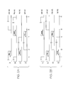
- FIGS. 2A and 2B are two alternate timing diagrams for controlling the switching sequence of the bridge transistors of FIG. 1 ;
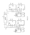
- FIG. 3 is a block diagram of a logic circuit for carrying out the control of this invention.
- the timing diagram of FIG. 2A graphically illustrates a first switching sequence of bridge transistors Q1-Q4 corresponding to the description of FIG. 1 set forth above.
- a full switching cycle occurs over the interval of t1-t5, with the first current reversal transition occurring in the interval t1-t2, and the second current reversal transition occurring in the interval t3-t4.
- the transistors in the left leg of the bridge (Q1 and Q2) carry the full free-wheeling current during the transition intervals
- transistors in the right leg of the bridge (Q3 and Q4) share the free-wheeling current with a respective free-wheeling diode D3 and D4.
- the average power dissipation of transistors that carry the full free-wheeling current (Q1 and Q2) is 33W
- the average power dissipation of transistors that share the free-wheeling current (Q3 and Q4) is 19W.
- the timing diagram of FIG. 2B illustrates a second switching sequence that is essentially the reverse of the first switching sequence illustrated by FIG. 2A .
- the transistors in the right leg of the bridge (Q3 and Q4) carry the full free-wheeling current during the transition intervals, and transistors in the left leg of the bridge (Q1 and Q2) share the free-wheeling current with a respective free-wheeling diode D1 and D2.
- the operation of the converter circuit is unchanged, but now the average power dissipation of transistors Q3 and Q4 is 33W, while the average power dissipation of transistors Q1 and Q2 is 19W.
- the control method of the present invention reduces the average power dissipation of the converter circuit by alternately driving the bridge transistors Q1-Q4 according to the first and second switching sequences of FIGS. 2A and 2B .
- the first switching sequence is used for a predetermined number N1 of cycles, whereafter the second switching sequence is used for a predetermined number N2 of cycles, and so on.
- the average power dissipated in each transistor will be the median or average of the two power dissipation levels ordinarily observed.
- the average power dissipation will now be (19W + 33W)/2, or 26W.
- the transistors Q1-Q4 can be designed to withstand an average power dissipation of 26W instead of 33W, a reduction of over 21%.
- the reduced power dissipation will improve transistor durability and reduce the transistor operating temperature (which in turn, reduces the on-resistance, and therefore the power dissipation).
- the power dissipation reduction may also permit savings in the converter packaging and heat sink.
- FIG. 3 depicts a suitable digital logic circuit.
- the reference numeral 10 generally designates a commercially available PS-ZVT bridge drive controller such as the UC3875 Phase Shift Resonant Controller produced by Texas Instruments, or equivalent.
- the controller 10 produces four phase-sequenced gate drive signals on lines 12, 14, 16, 18 for the four transistors of a full bridge circuit such as shown in FIG. 1 .
- the gate drive signals are identified as UL (for the upper left transistor Q1), LL (for the lower left transistor Q2), UR (for the upper right transistor Q3) and LR (for the lower right transistor Q4).
- the gate drive signals for the diagonally opposed bridge transistors can be reversed to provide an alternate mode of operation in which the power dissipated by the transistors in the right and left legs of the bridge will be reversed.
- the gate signals UL and LR are applied to the input ports IN0 and IN1 of 2:1 multiplexers (MUX) 20 and 22; and the gate signals UR and LL are applied to the input ports IN0 and IN1 of 2:1 multiplexers (MUX) 24 and 26.
- the outputs of MUXs 20 and 22 are coupled to the diagonally opposed bridge transistors Q1 and Q4, respectively; and the outputs of MUXs 24 and 26 are coupled to the diagonally opposed bridge transistors Q3 and Q2, respectively.
- a first Modulo-N counter 28 clocked by the UL signal on line 12 controls the logic level at the select input (SEL) of MUX 22; inverter 30 applies a signal of the opposite logic level to the select input (SEL) of MUX 20.
- a second Modulo-N counter 32 clocked by the UR signal on line 16 controls the logic level at the select input (SEL) of MUX 26; inverter 34 applies a signal of the opposite logic level to the select input (SEL) of MUX 24.
- the Modulo-N counters 28 and 32 both count the number of switching cycles of the bridge converter, but with a one-half cycle phase shift. Each counter operates at a 50% duty cycle as illustrated, producing a logic-one output for N switching cycles followed by a logic-zero output for N switching cycles, and so on.
- the gate signals UL, LR, UR and LL control the transistors Q1, Q4, Q3 and Q2, respectively, to carry out the switching sequence of FIG. 2A .
- the gate drive signals LR, UL, LL and UR control the transistors Q1, Q4, Q3 and Q2, respectively, to carry out the switching sequence of FIG. 2B .
- control of the present invention provides a way of reducing the maximum average power dissipated in the switching devices of a PS-ZVT bridge converter. This allows the use of identical lower-wattage devices in place of higher-wattage devices required for the traditional control, while preserving the high efficiency and low switching loss (and EMI) provided by ZVS circuit topologies. Additional savings may be realized in the thermal interface material of the converter package, and the package size can be reduced as well.
Landscapes
- Engineering & Computer Science (AREA)
- Power Engineering (AREA)
- Inverter Devices (AREA)
Applications Claiming Priority (1)
| Application Number | Priority Date | Filing Date | Title |
|---|---|---|---|
| US11/807,718 US7652899B2 (en) | 2007-05-30 | 2007-05-30 | Switching sequence control method for a PS-ZVT bridge converter |
Publications (3)
| Publication Number | Publication Date |
|---|---|
| EP1998432A2 true EP1998432A2 (de) | 2008-12-03 |
| EP1998432A3 EP1998432A3 (de) | 2016-06-15 |
| EP1998432B1 EP1998432B1 (de) | 2017-02-22 |
Family
ID=39712074
Family Applications (1)
| Application Number | Title | Priority Date | Filing Date |
|---|---|---|---|
| EP08155196.2A Active EP1998432B1 (de) | 2007-05-30 | 2008-04-25 | Steuerverfahren für Schaltsequenzen für einen PS-ZVT-Brückenwandler |
Country Status (2)
| Country | Link |
|---|---|
| US (1) | US7652899B2 (de) |
| EP (1) | EP1998432B1 (de) |
Cited By (9)
| Publication number | Priority date | Publication date | Assignee | Title |
|---|---|---|---|---|
| WO2013173075A1 (en) * | 2012-05-18 | 2013-11-21 | General Electric Company | Power converter and method |
| RU2518093C1 (ru) * | 2012-05-31 | 2014-06-10 | Делта Электроникс, Инк. | Устройство управления и способ управления, используемые при шунтировании блоков питания |
| CN104779805A (zh) * | 2015-04-16 | 2015-07-15 | 陕西科技大学 | 一种宽负载范围的移相全桥zvs变换器 |
| JP2016127779A (ja) * | 2015-01-08 | 2016-07-11 | 株式会社豊田中央研究所 | 電源システム |
| EP3041122A4 (de) * | 2013-08-26 | 2016-09-14 | Panasonic Ip Man Co Ltd | Steuerschaltung, schaltkreis, leistungsumwandlungsvorrichtung, ladevorrichtung, fahrzeug und steuerungsverfahren |
| JP2017139898A (ja) * | 2016-02-04 | 2017-08-10 | オムロンオートモーティブエレクトロニクス株式会社 | 電力変換装置 |
| US10005355B2 (en) | 2014-01-28 | 2018-06-26 | General Electric Company | Integrated mounting and cooling apparatus, electronic device, and vehicle |
| US10073512B2 (en) | 2014-11-19 | 2018-09-11 | General Electric Company | System and method for full range control of dual active bridge |
| US11063533B2 (en) | 2017-06-20 | 2021-07-13 | Koninklijke Philips N.V. | Control circuit for controlling a resonant power converter |
Families Citing this family (10)
| Publication number | Priority date | Publication date | Assignee | Title |
|---|---|---|---|---|
| US7652899B2 (en) * | 2007-05-30 | 2010-01-26 | Delphi Technologies, Inc. | Switching sequence control method for a PS-ZVT bridge converter |
| WO2011038227A1 (en) * | 2009-09-25 | 2011-03-31 | Greenray, Inc. | Modified zero voltage transition (zvt) full bridge converter and photovoltaic (pv) array using the same |
| TW201427246A (zh) * | 2012-12-26 | 2014-07-01 | Yen-Shin Lai | 相移全橋轉換裝置及控制方法 |
| US9263960B2 (en) * | 2013-09-16 | 2016-02-16 | Delta Electronics, Inc. | Power converters for wide input or output voltage range and control methods thereof |
| CN103812359B (zh) * | 2014-01-16 | 2016-08-17 | 深圳市保益新能电气有限公司 | 一种交流-直流变换电路及其控制方法 |
| CN110557022B (zh) * | 2018-05-31 | 2021-05-14 | 华为技术有限公司 | 控制psfb变换器的方法及psfb变换器 |
| DE102019212887A1 (de) * | 2019-08-28 | 2021-03-04 | Robert Bosch Gmbh | Ansteuerverfahren für einen Gleichspannungswandler und Gleichspannungswandler |
| JP2021069165A (ja) * | 2019-10-21 | 2021-04-30 | 株式会社オートネットワーク技術研究所 | 絶縁型dcdcコンバータ |
| EP4712307A1 (de) * | 2024-09-11 | 2026-03-18 | WiTricity AI Tech, LLC | Sequenzwechsel in vollbrückenumrichtern |
| US20260088698A1 (en) | 2024-09-20 | 2026-03-26 | Caterpillar Inc. | Dynamic control strategy for two-level dc-dc converters |
Citations (1)
| Publication number | Priority date | Publication date | Assignee | Title |
|---|---|---|---|---|
| US4864479A (en) | 1988-03-07 | 1989-09-05 | General Electric Company | Full-bridge lossless switching converter |
Family Cites Families (7)
| Publication number | Priority date | Publication date | Assignee | Title |
|---|---|---|---|---|
| US4201957A (en) * | 1977-09-21 | 1980-05-06 | Qualidyne Systems, Inc. | Power inverter having parallel switching elements |
| US5060130A (en) * | 1990-08-23 | 1991-10-22 | General Electric Company | High-efficiency, high-density, power supply including an input boost power supply |
| US5546294A (en) * | 1995-07-24 | 1996-08-13 | General Electric Company | Resonant converter with wide load range |
| US6069808A (en) * | 1997-05-21 | 2000-05-30 | Texas Instruments Incorporated | Symmetrical space vector PWM DC-AC converter controller |
| US6519168B2 (en) * | 2000-07-24 | 2003-02-11 | Chippower.Com, Inc. | High frequency DC to AC inverter |
| US6469491B1 (en) * | 2000-11-15 | 2002-10-22 | Peco Ii, Inc. | Apparatus and method for measuring DC load current of a switching power supply |
| US7652899B2 (en) * | 2007-05-30 | 2010-01-26 | Delphi Technologies, Inc. | Switching sequence control method for a PS-ZVT bridge converter |
-
2007
- 2007-05-30 US US11/807,718 patent/US7652899B2/en active Active
-
2008
- 2008-04-25 EP EP08155196.2A patent/EP1998432B1/de active Active
Patent Citations (1)
| Publication number | Priority date | Publication date | Assignee | Title |
|---|---|---|---|---|
| US4864479A (en) | 1988-03-07 | 1989-09-05 | General Electric Company | Full-bridge lossless switching converter |
Cited By (11)
| Publication number | Priority date | Publication date | Assignee | Title |
|---|---|---|---|---|
| WO2013173075A1 (en) * | 2012-05-18 | 2013-11-21 | General Electric Company | Power converter and method |
| US9270189B2 (en) | 2012-05-18 | 2016-02-23 | General Electric Company | Power converter and method |
| RU2518093C1 (ru) * | 2012-05-31 | 2014-06-10 | Делта Электроникс, Инк. | Устройство управления и способ управления, используемые при шунтировании блоков питания |
| EP3041122A4 (de) * | 2013-08-26 | 2016-09-14 | Panasonic Ip Man Co Ltd | Steuerschaltung, schaltkreis, leistungsumwandlungsvorrichtung, ladevorrichtung, fahrzeug und steuerungsverfahren |
| JPWO2015029374A1 (ja) * | 2013-08-26 | 2017-03-02 | パナソニックIpマネジメント株式会社 | 制御回路、スイッチング回路、電力変換装置、充電装置、車両、および、制御方法 |
| US10005355B2 (en) | 2014-01-28 | 2018-06-26 | General Electric Company | Integrated mounting and cooling apparatus, electronic device, and vehicle |
| US10073512B2 (en) | 2014-11-19 | 2018-09-11 | General Electric Company | System and method for full range control of dual active bridge |
| JP2016127779A (ja) * | 2015-01-08 | 2016-07-11 | 株式会社豊田中央研究所 | 電源システム |
| CN104779805A (zh) * | 2015-04-16 | 2015-07-15 | 陕西科技大学 | 一种宽负载范围的移相全桥zvs变换器 |
| JP2017139898A (ja) * | 2016-02-04 | 2017-08-10 | オムロンオートモーティブエレクトロニクス株式会社 | 電力変換装置 |
| US11063533B2 (en) | 2017-06-20 | 2021-07-13 | Koninklijke Philips N.V. | Control circuit for controlling a resonant power converter |
Also Published As
| Publication number | Publication date |
|---|---|
| EP1998432B1 (de) | 2017-02-22 |
| EP1998432A3 (de) | 2016-06-15 |
| US7652899B2 (en) | 2010-01-26 |
| US20080298087A1 (en) | 2008-12-04 |
Similar Documents
| Publication | Publication Date | Title |
|---|---|---|
| EP1998432B1 (de) | Steuerverfahren für Schaltsequenzen für einen PS-ZVT-Brückenwandler | |
| US10171004B2 (en) | DC-DC converter | |
| US6353547B1 (en) | Three-level soft-switched converters | |
| US8149596B2 (en) | N-phase full bridge power converter | |
| CN109874375B (zh) | 电力变换装置 | |
| CN1783687B (zh) | 用于减少同步整流器的体二极管传导的方法和装置 | |
| JP7142609B2 (ja) | 電力変換装置 | |
| US20010036088A1 (en) | Efficient power conversion circuit having zero voltage switching | |
| JP6355187B2 (ja) | 電力変換装置 | |
| JP6849373B2 (ja) | 双方向絶縁型dc/dcコンバータ | |
| EP3326282A1 (de) | Resonanzsystemsteuergerät und zyklusweise prädiktive weichschaltung | |
| JP3463807B2 (ja) | Dc−dcコンバータ | |
| US11606025B2 (en) | Bridge rectifier operation and power factor correction circuit | |
| JP2003111413A (ja) | 双方向dc−dcコンバータ | |
| CN115528939B (zh) | 包括逆变全桥的转换器及其控制方法 | |
| JP4783905B2 (ja) | ゼロボルテージスイッチング高周波インバーター | |
| JP2001025259A (ja) | Pwmインバーター装置 | |
| CN112350598B (zh) | 一种谐振零电流电路 | |
| KR101749826B1 (ko) | 커플드 인덕터를 갖는 영전압 스위칭 풀-브릿지 인버터 | |
| JP7144591B2 (ja) | 電力変換装置 | |
| CN104218837B (zh) | 用于将dc电压转换成ac电压的方法和系统 | |
| JP2001037221A (ja) | 電源装置 | |
| KR20050086024A (ko) | 직류-직류 변환 장치 | |
| KR100573114B1 (ko) | 플라즈마 디스플레이 장치용 비대칭 하프브리지 컨버터 | |
| JP2020022299A (ja) | 電源装置 |
Legal Events
| Date | Code | Title | Description |
|---|---|---|---|
| PUAI | Public reference made under article 153(3) epc to a published international application that has entered the european phase |
Free format text: ORIGINAL CODE: 0009012 |
|
| AK | Designated contracting states |
Kind code of ref document: A2 Designated state(s): AT BE BG CH CY CZ DE DK EE ES FI FR GB GR HR HU IE IS IT LI LT LU LV MC MT NL NO PL PT RO SE SI SK TR |
|
| AX | Request for extension of the european patent |
Extension state: AL BA MK RS |
|
| PUAL | Search report despatched |
Free format text: ORIGINAL CODE: 0009013 |
|
| AK | Designated contracting states |
Kind code of ref document: A3 Designated state(s): AT BE BG CH CY CZ DE DK EE ES FI FR GB GR HR HU IE IS IT LI LT LU LV MC MT NL NO PL PT RO SE SI SK TR |
|
| AX | Request for extension of the european patent |
Extension state: AL BA MK RS |
|
| RIC1 | Information provided on ipc code assigned before grant |
Ipc: H02M 7/5387 20070101AFI20160510BHEP |
|
| 17P | Request for examination filed |
Effective date: 20160704 |
|
| GRAP | Despatch of communication of intention to grant a patent |
Free format text: ORIGINAL CODE: EPIDOSNIGR1 |
|
| RIC1 | Information provided on ipc code assigned before grant |
Ipc: H02M 1/32 20070101ALI20161108BHEP Ipc: H02M 7/5388 20070101ALN20161108BHEP Ipc: H02M 7/5387 20070101AFI20161108BHEP |
|
| INTG | Intention to grant announced |
Effective date: 20161207 |
|
| GRAS | Grant fee paid |
Free format text: ORIGINAL CODE: EPIDOSNIGR3 |
|
| GRAA | (expected) grant |
Free format text: ORIGINAL CODE: 0009210 |
|
| RBV | Designated contracting states (corrected) |
Designated state(s): AT BE BG CH CY CZ DE DK EE ES FI FR GB GR HR HU IE IS IT LI LT LU LV MC MT NL NO PL PT RO SE SI SK TR |
|
| AK | Designated contracting states |
Kind code of ref document: B1 Designated state(s): AT BE BG CH CY CZ DE DK EE ES FI FR GB GR HR HU IE IS IT LI LT LU LV MC MT NL NO PL PT RO SE SI SK TR |
|
| AKX | Designation fees paid |
Designated state(s): AT BE BG CH CY CZ DE DK EE ES FI FR GB GR HR HU IE IS IT LI LT LU LV MC MT NL NO PL PT RO SE SI SK TR |
|
| REG | Reference to a national code |
Ref country code: GB Ref legal event code: FG4D |
|
| REG | Reference to a national code |
Ref country code: CH Ref legal event code: EP |
|
| REG | Reference to a national code |
Ref country code: AT Ref legal event code: REF Ref document number: 869982 Country of ref document: AT Kind code of ref document: T Effective date: 20170315 |
|
| REG | Reference to a national code |
Ref country code: IE Ref legal event code: FG4D |
|
| REG | Reference to a national code |
Ref country code: DE Ref legal event code: R096 Ref document number: 602008048807 Country of ref document: DE |
|
| REG | Reference to a national code |
Ref country code: LT Ref legal event code: MG4D |
|
| REG | Reference to a national code |
Ref country code: NL Ref legal event code: MP Effective date: 20170222 |
|
| REG | Reference to a national code |
Ref country code: AT Ref legal event code: MK05 Ref document number: 869982 Country of ref document: AT Kind code of ref document: T Effective date: 20170222 |
|
| PG25 | Lapsed in a contracting state [announced via postgrant information from national office to epo] |
Ref country code: HR Free format text: LAPSE BECAUSE OF FAILURE TO SUBMIT A TRANSLATION OF THE DESCRIPTION OR TO PAY THE FEE WITHIN THE PRESCRIBED TIME-LIMIT Effective date: 20170222 Ref country code: GR Free format text: LAPSE BECAUSE OF FAILURE TO SUBMIT A TRANSLATION OF THE DESCRIPTION OR TO PAY THE FEE WITHIN THE PRESCRIBED TIME-LIMIT Effective date: 20170523 Ref country code: LT Free format text: LAPSE BECAUSE OF FAILURE TO SUBMIT A TRANSLATION OF THE DESCRIPTION OR TO PAY THE FEE WITHIN THE PRESCRIBED TIME-LIMIT Effective date: 20170222 Ref country code: NO Free format text: LAPSE BECAUSE OF FAILURE TO SUBMIT A TRANSLATION OF THE DESCRIPTION OR TO PAY THE FEE WITHIN THE PRESCRIBED TIME-LIMIT Effective date: 20170522 Ref country code: FI Free format text: LAPSE BECAUSE OF FAILURE TO SUBMIT A TRANSLATION OF THE DESCRIPTION OR TO PAY THE FEE WITHIN THE PRESCRIBED TIME-LIMIT Effective date: 20170222 |
|
| PG25 | Lapsed in a contracting state [announced via postgrant information from national office to epo] |
Ref country code: ES Free format text: LAPSE BECAUSE OF FAILURE TO SUBMIT A TRANSLATION OF THE DESCRIPTION OR TO PAY THE FEE WITHIN THE PRESCRIBED TIME-LIMIT Effective date: 20170222 Ref country code: SE Free format text: LAPSE BECAUSE OF FAILURE TO SUBMIT A TRANSLATION OF THE DESCRIPTION OR TO PAY THE FEE WITHIN THE PRESCRIBED TIME-LIMIT Effective date: 20170222 Ref country code: LV Free format text: LAPSE BECAUSE OF FAILURE TO SUBMIT A TRANSLATION OF THE DESCRIPTION OR TO PAY THE FEE WITHIN THE PRESCRIBED TIME-LIMIT Effective date: 20170222 Ref country code: BG Free format text: LAPSE BECAUSE OF FAILURE TO SUBMIT A TRANSLATION OF THE DESCRIPTION OR TO PAY THE FEE WITHIN THE PRESCRIBED TIME-LIMIT Effective date: 20170522 Ref country code: NL Free format text: LAPSE BECAUSE OF FAILURE TO SUBMIT A TRANSLATION OF THE DESCRIPTION OR TO PAY THE FEE WITHIN THE PRESCRIBED TIME-LIMIT Effective date: 20170222 Ref country code: AT Free format text: LAPSE BECAUSE OF FAILURE TO SUBMIT A TRANSLATION OF THE DESCRIPTION OR TO PAY THE FEE WITHIN THE PRESCRIBED TIME-LIMIT Effective date: 20170222 Ref country code: PT Free format text: LAPSE BECAUSE OF FAILURE TO SUBMIT A TRANSLATION OF THE DESCRIPTION OR TO PAY THE FEE WITHIN THE PRESCRIBED TIME-LIMIT Effective date: 20170622 |
|
| PG25 | Lapsed in a contracting state [announced via postgrant information from national office to epo] |
Ref country code: RO Free format text: LAPSE BECAUSE OF FAILURE TO SUBMIT A TRANSLATION OF THE DESCRIPTION OR TO PAY THE FEE WITHIN THE PRESCRIBED TIME-LIMIT Effective date: 20170222 Ref country code: EE Free format text: LAPSE BECAUSE OF FAILURE TO SUBMIT A TRANSLATION OF THE DESCRIPTION OR TO PAY THE FEE WITHIN THE PRESCRIBED TIME-LIMIT Effective date: 20170222 Ref country code: SK Free format text: LAPSE BECAUSE OF FAILURE TO SUBMIT A TRANSLATION OF THE DESCRIPTION OR TO PAY THE FEE WITHIN THE PRESCRIBED TIME-LIMIT Effective date: 20170222 Ref country code: IT Free format text: LAPSE BECAUSE OF FAILURE TO SUBMIT A TRANSLATION OF THE DESCRIPTION OR TO PAY THE FEE WITHIN THE PRESCRIBED TIME-LIMIT Effective date: 20170222 Ref country code: CZ Free format text: LAPSE BECAUSE OF FAILURE TO SUBMIT A TRANSLATION OF THE DESCRIPTION OR TO PAY THE FEE WITHIN THE PRESCRIBED TIME-LIMIT Effective date: 20170222 |
|
| REG | Reference to a national code |
Ref country code: DE Ref legal event code: R097 Ref document number: 602008048807 Country of ref document: DE |
|
| PG25 | Lapsed in a contracting state [announced via postgrant information from national office to epo] |
Ref country code: DK Free format text: LAPSE BECAUSE OF FAILURE TO SUBMIT A TRANSLATION OF THE DESCRIPTION OR TO PAY THE FEE WITHIN THE PRESCRIBED TIME-LIMIT Effective date: 20170222 Ref country code: PL Free format text: LAPSE BECAUSE OF FAILURE TO SUBMIT A TRANSLATION OF THE DESCRIPTION OR TO PAY THE FEE WITHIN THE PRESCRIBED TIME-LIMIT Effective date: 20170222 |
|
| REG | Reference to a national code |
Ref country code: CH Ref legal event code: PL |
|
| PLBE | No opposition filed within time limit |
Free format text: ORIGINAL CODE: 0009261 |
|
| STAA | Information on the status of an ep patent application or granted ep patent |
Free format text: STATUS: NO OPPOSITION FILED WITHIN TIME LIMIT |
|
| GBPC | Gb: european patent ceased through non-payment of renewal fee |
Effective date: 20170522 |
|
| REG | Reference to a national code |
Ref country code: IE Ref legal event code: MM4A |
|
| REG | Reference to a national code |
Ref country code: FR Ref legal event code: ST Effective date: 20171229 |
|
| 26N | No opposition filed |
Effective date: 20171123 |
|
| PG25 | Lapsed in a contracting state [announced via postgrant information from national office to epo] |
Ref country code: MC Free format text: LAPSE BECAUSE OF FAILURE TO SUBMIT A TRANSLATION OF THE DESCRIPTION OR TO PAY THE FEE WITHIN THE PRESCRIBED TIME-LIMIT Effective date: 20170222 Ref country code: FR Free format text: LAPSE BECAUSE OF NON-PAYMENT OF DUE FEES Effective date: 20170502 |
|
| PG25 | Lapsed in a contracting state [announced via postgrant information from national office to epo] |
Ref country code: LU Free format text: LAPSE BECAUSE OF NON-PAYMENT OF DUE FEES Effective date: 20170425 Ref country code: SI Free format text: LAPSE BECAUSE OF FAILURE TO SUBMIT A TRANSLATION OF THE DESCRIPTION OR TO PAY THE FEE WITHIN THE PRESCRIBED TIME-LIMIT Effective date: 20170222 Ref country code: CH Free format text: LAPSE BECAUSE OF NON-PAYMENT OF DUE FEES Effective date: 20170430 Ref country code: LI Free format text: LAPSE BECAUSE OF NON-PAYMENT OF DUE FEES Effective date: 20170430 |
|
| REG | Reference to a national code |
Ref country code: BE Ref legal event code: MM Effective date: 20170430 |
|
| PG25 | Lapsed in a contracting state [announced via postgrant information from national office to epo] |
Ref country code: GB Free format text: LAPSE BECAUSE OF NON-PAYMENT OF DUE FEES Effective date: 20170522 Ref country code: IE Free format text: LAPSE BECAUSE OF NON-PAYMENT OF DUE FEES Effective date: 20170425 |
|
| PG25 | Lapsed in a contracting state [announced via postgrant information from national office to epo] |
Ref country code: BE Free format text: LAPSE BECAUSE OF NON-PAYMENT OF DUE FEES Effective date: 20170430 |
|
| PG25 | Lapsed in a contracting state [announced via postgrant information from national office to epo] |
Ref country code: MT Free format text: LAPSE BECAUSE OF NON-PAYMENT OF DUE FEES Effective date: 20170425 |
|
| REG | Reference to a national code |
Ref country code: DE Ref legal event code: R081 Ref document number: 602008048807 Country of ref document: DE Owner name: DELPHI TECHNOLOGIES IP LIMITED, BB Free format text: FORMER OWNER: DELPHI TECHNOLOGIES, INC., TROY, MICH., US |
|
| PG25 | Lapsed in a contracting state [announced via postgrant information from national office to epo] |
Ref country code: HU Free format text: LAPSE BECAUSE OF FAILURE TO SUBMIT A TRANSLATION OF THE DESCRIPTION OR TO PAY THE FEE WITHIN THE PRESCRIBED TIME-LIMIT; INVALID AB INITIO Effective date: 20080425 |
|
| PG25 | Lapsed in a contracting state [announced via postgrant information from national office to epo] |
Ref country code: CY Free format text: LAPSE BECAUSE OF NON-PAYMENT OF DUE FEES Effective date: 20170222 |
|
| PG25 | Lapsed in a contracting state [announced via postgrant information from national office to epo] |
Ref country code: TR Free format text: LAPSE BECAUSE OF FAILURE TO SUBMIT A TRANSLATION OF THE DESCRIPTION OR TO PAY THE FEE WITHIN THE PRESCRIBED TIME-LIMIT Effective date: 20170222 |
|
| PG25 | Lapsed in a contracting state [announced via postgrant information from national office to epo] |
Ref country code: IS Free format text: LAPSE BECAUSE OF FAILURE TO SUBMIT A TRANSLATION OF THE DESCRIPTION OR TO PAY THE FEE WITHIN THE PRESCRIBED TIME-LIMIT Effective date: 20170622 |
|
| P01 | Opt-out of the competence of the unified patent court (upc) registered |
Effective date: 20230327 |
|
| PGFP | Annual fee paid to national office [announced via postgrant information from national office to epo] |
Ref country code: DE Payment date: 20250317 Year of fee payment: 18 |