EP2000945B1 - Lecteur de carte protégé contre la manipulation - Google Patents
Lecteur de carte protégé contre la manipulation Download PDFInfo
- Publication number
- EP2000945B1 EP2000945B1 EP07010877A EP07010877A EP2000945B1 EP 2000945 B1 EP2000945 B1 EP 2000945B1 EP 07010877 A EP07010877 A EP 07010877A EP 07010877 A EP07010877 A EP 07010877A EP 2000945 B1 EP2000945 B1 EP 2000945B1
- Authority
- EP
- European Patent Office
- Prior art keywords
- conductor path
- card reader
- path element
- bendable
- exposed
- Prior art date
- Legal status (The legal status is an assumption and is not a legal conclusion. Google has not performed a legal analysis and makes no representation as to the accuracy of the status listed.)
- Ceased
Links
Images


Classifications
-
- G—PHYSICS
- G06—COMPUTING OR CALCULATING; COUNTING
- G06K—GRAPHICAL DATA READING; PRESENTATION OF DATA; RECORD CARRIERS; HANDLING RECORD CARRIERS
- G06K7/00—Methods or arrangements for sensing record carriers, e.g. for reading patterns
- G06K7/0013—Methods or arrangements for sensing record carriers, e.g. for reading patterns by galvanic contacts, e.g. card connectors for ISO-7816 compliant smart cards or memory cards, e.g. SD card readers
- G06K7/0021—Methods or arrangements for sensing record carriers, e.g. for reading patterns by galvanic contacts, e.g. card connectors for ISO-7816 compliant smart cards or memory cards, e.g. SD card readers for reading/sensing record carriers having surface contacts
Definitions
- the present invention relates to a card reader, in particular chip card reader, with a contacting unit for a card inserted through a card insertion opening.
- EP 0 889 493 A2 known card reader is a SIM card reader with a limit switch, which detects whether a card has been inserted.
- the limit switch consists of two metal contacts, which are connected by the card.
- This SIM card reader is mounted on a circuit board.
- a card reader with a manually operable drawer known which has two end positions. In one end position, the insertion or removal of a chip card is possible, while in the other end position, the chip card is connected by a contact unit for a user inaccessible to a reading and writing device. An end contact is positioned so that it is open when the drawer is pulled out and closes only when the drawer has reached its closed end position.
- a tamper-protected card reader is known, which is arranged in a pocket from a Bohrschutzfolie with fine mesh conductor track structure. If the bag is removed or destroyed by drilling, for example, the conductor tracks of the protective film are destroyed and the manipulation can be detected.
- This card reader is also mounted on a circuit board.
- the data exchange with a card can be manipulated by unseating the card reader soldered on a customer board and from the customer board is lifted and the now accessible electrical contacts of the contacting are contacted.
- the object of the present invention is to protect a card reader of the type mentioned above from such lifting, i. to provide a "secure card reader”.
- the portions of the bendable strip conductor element which lie between the fold line and the exposed contacts are bent by more than 90 °, but less than 180 °, relative to the fold line, whereby the two exposed contacts are spaced apart from one another. If the card reader is placed on the customer circuit board, the bendable strip conductor element between the card reader and customer circuit board is further bent until the two exposed contacts abut each other electrically and thus the switch formed by the two exposed contacts is closed. If the card reader is unsoldered or even removed from the customer PCB for tampering purposes, the two exposed contacts lift off each other at the slightest lift of the card reader due to the elastic restoring force, and the switch opens. This is detected by a control unit of the customer board, which then no longer permits read operation or deactivates the contactor unit. An unnoticed manipulation of the contacting unit is thus not possible, so that a "tamper-proof" card reader is made possible.
- the contacting unit is preferably surrounded by a drill protection pocket which is open at the card insertion opening and has a fine-meshed conductor track structure with at least one continuous conductor track and a recess provided on the attachment side of the card reader within which the bendable conductor track element is provided.
- the bag is made at least one conductor foil formed, which also has the bendable conductor element. If the bag is removed or destroyed by drilling, for example, the at least one continuous track, over which a current flows during operation, is severed. This is also recognized by the control unit of the customer circuit board, which then no longer permits read operation or deactivates the contactor unit.
- the drill protection bag is formed from a one-piece strip conductor blank which has the fine-meshed strip conductor structure, which forms the at least one continuous strip in the erected state of the bag, and the bendable strip conductor element with its two exposed contacts.
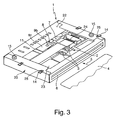
- the in Fig. 1 to 3 1 has a contact-making unit 2 with electrical contact springs 3 in order to contact electrical contact fields (not shown) of a chip card 4 introduced into the contacting unit 2.
- the smart card 4 carries a microchip (not shown) for storing data, the contacts of which are provided as electrical contact pads on the card surface.
- the smart card 4 is inserted by the user in the insertion direction 5 via a card insertion opening 6 into its data exchange position in the contacting unit 2 and after data exchange by the user again pulled out of the contacting unit 2 (so-called push / pull card reader).
- the card reader 1 has on its base or fastening side 7 a strip conductor element 8 which can be bent over against the action of an elastic restoring force with two exposed electrical contacts (eg gold contacts) 9a, 9b .
- the conductor track element 8 is formed by a single-sided, single-layer strip conductor strip, the conductor tracks of which as well as the exposed contacts 9a, 9b are provided on the fastening side 7 facing strip side.
- the bendable strip conductor element 8 is divided into three sections, namely a first section 8a, which is attached to the card reader housing 12 , a second section 8b, which adjoins the first section 8a and has an exposed contact 9a, and a third portion 8c which adjoins the second portion 8b and has the other exposed contact 9b.
- a first section 8a which is attached to the card reader housing 12
- a second section 8b which adjoins the first section 8a and has an exposed contact 9a
- a third portion 8c which adjoins the second portion 8b and has the other exposed contact 9b.
- the second portion 8b is bent around the fold line 10 in abutment against the first portion 8a and adhered thereto.
- the first section 8a may be glued to the attachment side 7.
- the third section 8c is bent so far around the fold line 11 in the direction of the second section 8b that it encloses an acute angle of, for example, 45 ° with the second section 8c and the two exposed contacts 9a, 9b now face each other, but still from each other are spaced.
- the card reader 1 is now placed with its attachment side 7 on a customer board 13 and soldered using four lateral contact legs 14 on the customer board 13 ( Fig. 1c ).
- the third section 8c against the action of the elastic restoring force further bent in the direction of the second section 8b until the two exposed contacts 9a, 9b finally electrically conductive abut each other and thus by the two exposed contacts 9a , 9b formed switch is closed. If the card reader 1 is unsoldered or even removed from the customer circuit board 13 for manipulation purposes, the two exposed contacts 9a, 9b lift off due to the elastic restoring force even at the slightest increase in the card reader 1, and the switch opens.
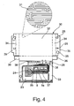
- the contacting unit 2 is of a at the Receiveein Fighting réelle 6 open Bohrschutz bag 20 ( FIG. Fig. 2 and 3 ) consisting of a single strip of conductor foil 30 ( FIG. Fig. 4 ) , which also has the bendable strip conductor element 8.
- the pocket 20 has nationwide a fine-meshed (eg meandering) conductor track structure with, for example, two continuous tracks 21 and provided on the pocket bottom 22 recess 23 , within which the terminals 24 of the card reader 1 and the bendable strip conductor element 8 are provided.
- the contact-making unit 2 has on the bottom side two pins 15 , which pass through corresponding holes 26 (FIG. Fig. 4 ) pass through the pocket 20 and so the bag Position 20 on the contacting unit 2.
- the strip conductor blank 30 has a surface-area interconnect structure with a plurality of open interconnects 31, which run at minimum distance from one another and form the continuous interconnects 22 in the erected state of the pocket 20, as well as the bendable strip conductor element 8.
- the strip conductor blank 30 has a cover section 32 forming the top of the pocket , a bottom section 33 with the recess 23 forming the underside of the pocket, three side wall sections 34 with two lateral overlapping sections 35 and two tab sections 36 , these sections being indicated by dash-dotted lines due to their flexibility Folding lines can be bent.
- the open traces 31 of the individual sections 32 to 36 are electrically connected to each other so as to form the two continuous traces 21.
- the bottom portion 33 has within its recess 23 formed as a strip conductor bendable conductor element 8 and a further strip conductor strip 37 , at its free flexible end, the connection contacts 24 are provided.
- ten soldering surfaces (soldering pads) 38 are provided in the bottom portion 33. These ten solder pads 38 and the four ends of the two continuous tracks 22 are connected to the terminals 24 via the tracks of the strip conductor 37.
- the two exposed contacts 9a, 9b of the bendable strip conductor element 8 are provided in one of the two continuous strip conductors 22, so that this strip conductor is interrupted when the contacts 9a, 9b are lifted apart from one another.
- the holes 25 for the contact legs 14 and the holes 26 for the pins 15 of the contacting unit 2 are provided.
- the card reader 1 is connected with its connection contacts 24 to a corresponding connector (eg Molex connector) of the customer circuit board 13 and then fixed by means of the contact legs 14 on the customer board 13.
- a corresponding connector eg Molex connector
- the bag 20 is removed or destroyed by drilling, for example, or when the contacting unit 2 is lifted from the customer board 13, one or more of them are removed both continuous strip conductors 21, over which a current flows during operation, cut through. This is detected by the control unit of the customer circuit board 13, which in this case no longer permits read operation or deactivates the contactor unit 2.
Landscapes
- Engineering & Computer Science (AREA)
- Artificial Intelligence (AREA)
- Computer Vision & Pattern Recognition (AREA)
- Physics & Mathematics (AREA)
- General Physics & Mathematics (AREA)
- Theoretical Computer Science (AREA)
- Coupling Device And Connection With Printed Circuit (AREA)
Claims (10)
- Lecteur de carte (1) avec une unité de contact (2) pour une carte pouvant être introduite à travers une ouverture d'introduction de carte (6),
caractérisé en ce
qu'il est prévu sur un côté de fixation (7) du lecteur de carte (1) prévu pour le montage sur une carte de circuit imprimé (13) un élément à pistes conductrices (8) pliable contre l'action d'une force de rappel élastique et présentant deux contacts électriques découverts (9a, 9b) qui sont prévus sur une piste conductrice (21) de l'élément à pistes conductrices pliable (8) comme commutateurs électriques pour interrompre ou connecter la piste conductrice (21),
que l'élément à pistes conductrices (8) peut être plié entre ses deux contacts découverts (9a, 9b) jusqu'à ce que les deux contacts découverts (9a, 9b) soient appliqués l'un contre l'autre de manière électroconductrice contre l'action de la force de rappel élastique et connectent la piste conductrice (21),
et que dans un état prêt à la fixation du lecteur de cartes (1) pour le montage sur la carte de circuit imprimé (13), l'élément à pistes conductrices (8) est plié entre ses deux contacts découverts (9a, 9b) de plus de 90° mais de moins de 180° et de ce fait les deux contacts découverts (9a, 9b) ne sont pas reliés entre eux électriquement. - Lecteur de carte selon la revendication 1, caractérisé en ce que l'élément à pistes conductrices pliable (8) présente une ligne de pliage (11) au moins entre ses deux contacts découverts (9a, 9b).
- Lecteur de carte selon la revendication 2, caractérisé en ce que dans un état prêt à la fixation du lecteur de cartes (1) les portions (8b, 8c) de l'élément à pistes conductrices pliable (8) respectivement situées entre la ligne de pliage (11) et les contacts découverts (9a, 9b) sont pliées de plus de 90° par rapport à la ligne de pliage (11).
- Lecteur de carte selon une des revendications précédentes, caractérisé en ce que l'élément à pistes conductrices pliable (8) est formé par une bande de piste conductrice fixée d'un côté.
- Lecteur de carte selon une des revendications précédentes, caractérisé en ce que l'élément à pistes conductrices pliable (8) est réalisé à une couche avec des pistes conductrices prévues seulement d'un côté ou à deux couches avec des pistes conductrices prévues des deux côtés.
- Lecteur de carte selon une des revendications précédentes, caractérisé en ce que l'élément à pistes conductrices pliable (8) comprend une première portion (8a) fixée d'un côté, une deuxième portion (8b) qui se raccorde à la première portion (8a) et présente un contact découvert (9a), et une troisième portion (8c) qui se raccorde à la deuxième portion (8b) et présente l'autre contact découvert (9a), les deux contacts découverts (9a, 9b) étant prévus du côté de l'élément à pistes conductrices pliable (8) tourné vers le côté de fixation (7), et que les trois portions (8a-8c) sont pliables ou pliées en Z.
- Lecteur de carte selon une des revendications précédentes, caractérisé en ce que l'unité de contact (2) est entourée par une cage de protection anti-perçage (20) ouverte à l'ouverture d'introduction de carte (6), qui présente une structure de pistes conductrices à mailles fines avec au moins une piste conductrice continue (22) ainsi que l'élément à pistes conductrices pliable (8).
- Lecteur de carte selon la revendication 7, caractérisé en ce que la cage (20) présente du côté inférieur de cage (22) formant le fond du lecteur de cartes (1) un évidement (23) à l'intérieur duquel l'élément à pistes conductrices pliable (8) est prévu.
- Lecteur de carte selon la revendication 7 ou 8, caractérisé en ce que la cage (20) est formée d'au moins une membrane à pistes conductrices (30) qui présente aussi l'élément à pistes conductrices pliable (8).
- Lecteur de cartes selon une des revendications 7 à 9, caractérisé en ce que la cage de protection anti-perçage (20) est formée d'une découpe de membrane à pistes conductrices (30) en une seule pièce qui présente la structure de pistes conductrices à mailles fines, laquelle, dans l'état monté de la cage (20), forme ladite au moins une piste conductrice continue (22) et présente l'élément à pistes conductrices pliable (8) avec ses deux contacts découverts (9a, 9b).
Priority Applications (3)
| Application Number | Priority Date | Filing Date | Title |
|---|---|---|---|
| DE502007004647T DE502007004647D1 (de) | 2007-06-01 | 2007-06-01 | Manipulationsgeschützter Kartenleser |
| EP07010877A EP2000945B1 (fr) | 2007-06-01 | 2007-06-01 | Lecteur de carte protégé contre la manipulation |
| US12/150,028 US20080296377A1 (en) | 2007-06-01 | 2008-04-24 | Tamper-proof card reader |
Applications Claiming Priority (1)
| Application Number | Priority Date | Filing Date | Title |
|---|---|---|---|
| EP07010877A EP2000945B1 (fr) | 2007-06-01 | 2007-06-01 | Lecteur de carte protégé contre la manipulation |
Publications (2)
| Publication Number | Publication Date |
|---|---|
| EP2000945A1 EP2000945A1 (fr) | 2008-12-10 |
| EP2000945B1 true EP2000945B1 (fr) | 2010-08-04 |
Family
ID=38474187
Family Applications (1)
| Application Number | Title | Priority Date | Filing Date |
|---|---|---|---|
| EP07010877A Ceased EP2000945B1 (fr) | 2007-06-01 | 2007-06-01 | Lecteur de carte protégé contre la manipulation |
Country Status (3)
| Country | Link |
|---|---|
| US (1) | US20080296377A1 (fr) |
| EP (1) | EP2000945B1 (fr) |
| DE (1) | DE502007004647D1 (fr) |
Cited By (1)
| Publication number | Priority date | Publication date | Assignee | Title |
|---|---|---|---|---|
| DE102011007296A1 (de) * | 2011-04-13 | 2012-10-18 | Zf Friedrichshafen Ag | Kartenleser für eine Chipkarte, Kartenlesergehäuse für den Kartenleser und Kartenlesesystem |
Families Citing this family (8)
| Publication number | Priority date | Publication date | Assignee | Title |
|---|---|---|---|---|
| CN102647855B (zh) * | 2011-02-16 | 2016-04-06 | 技嘉科技股份有限公司 | 切板机的辅助夹板治具 |
| US9122937B2 (en) * | 2012-07-23 | 2015-09-01 | Fci Americas Technology Llc | Tamper-resistant housing assembly |
| US9298956B2 (en) * | 2013-10-04 | 2016-03-29 | Square, Inc. | Tamper protection mesh in an electronic device |
| US10706400B1 (en) * | 2015-11-19 | 2020-07-07 | Wells Fargo Bank, N.A. | Systems and methods for financial operations performed at a contactless ATM |
| US10535047B1 (en) | 2015-11-19 | 2020-01-14 | Wells Fargo Bank N.A. | Systems and methods for financial operations performed at a contactless ATM |
| US10192076B1 (en) | 2016-08-29 | 2019-01-29 | Square, Inc. | Security housing with recesses for tamper localization |
| US10504096B1 (en) | 2017-04-28 | 2019-12-10 | Square, Inc. | Tamper detection using ITO touch screen traces |
| EP3495984A1 (fr) * | 2017-12-05 | 2019-06-12 | ddm hopt + schuler GmbH & Co. KG. | Lecteur de carte protégé contre la manipulation doté d'un couvercle de protection d'alésage |
Family Cites Families (9)
| Publication number | Priority date | Publication date | Assignee | Title |
|---|---|---|---|---|
| FR2625349B1 (fr) * | 1987-12-28 | 1991-06-07 | Schlumberger Ind Sa | Dispositif de lecture/ecriture pour cartes a memoire muni d'un dispositif anti fraude |
| DE3916783A1 (de) * | 1988-10-19 | 1990-04-26 | Landis & Gyr Ag | Vorrichtung zum lesen und/oder beschreiben von chip-karten |
| DE9105960U1 (de) * | 1991-05-14 | 1992-06-11 | Siemens Nixdorf Informationssysteme AG, 4790 Paderborn | Schutzvorrichtung für Schaltungsteile und/oder Daten in einem Gerät zur Authentifikation und Betragsbestätigung |
| DE19502176A1 (de) * | 1995-01-25 | 1996-08-08 | Thomas & Betts Gmbh | Chipkarten-Lesegerät |
| US5834756A (en) * | 1996-06-03 | 1998-11-10 | Motorola, Inc. | Magnetically communicative card |
| US6326568B2 (en) * | 1997-07-02 | 2001-12-04 | Molex Incorporated | Blade switch assembly for a card reader |
| FR2771834B1 (fr) * | 1997-12-03 | 2000-01-21 | Socapex Amphenol | Dispositif de connexion electrique pour cooperer avec un support electronique mobile |
| DE202006009983U1 (de) * | 2006-06-23 | 2006-08-24 | Ddm Hopt + Schuler Gmbh & Co. Kg | Manipulationsgeschützter Kartenleser |
| DE202007001626U1 (de) * | 2007-02-06 | 2007-04-19 | Ddm Hopt + Schuler Gmbh & Co. Kg | Kartenleser mit Manipulationserkennung |
-
2007
- 2007-06-01 EP EP07010877A patent/EP2000945B1/fr not_active Ceased
- 2007-06-01 DE DE502007004647T patent/DE502007004647D1/de active Active
-
2008
- 2008-04-24 US US12/150,028 patent/US20080296377A1/en not_active Abandoned
Cited By (1)
| Publication number | Priority date | Publication date | Assignee | Title |
|---|---|---|---|---|
| DE102011007296A1 (de) * | 2011-04-13 | 2012-10-18 | Zf Friedrichshafen Ag | Kartenleser für eine Chipkarte, Kartenlesergehäuse für den Kartenleser und Kartenlesesystem |
Also Published As
| Publication number | Publication date |
|---|---|
| DE502007004647D1 (de) | 2010-09-16 |
| US20080296377A1 (en) | 2008-12-04 |
| EP2000945A1 (fr) | 2008-12-10 |
Similar Documents
| Publication | Publication Date | Title |
|---|---|---|
| EP2000945B1 (fr) | Lecteur de carte protégé contre la manipulation | |
| DE69018253T2 (de) | IC Speicherkarte. | |
| DE69510620T2 (de) | Kassette für Spielmaschine | |
| DE60301099T2 (de) | Elektrischer Verbinder für eine Kamera | |
| DE102006018610A1 (de) | Schlanke elektronische USB-Vorrichtung | |
| EP1816583B1 (fr) | Dispositif de contact pour une carte à puce | |
| CH661816A5 (de) | Traeger mit einem ic-baustein. | |
| EP1873680A1 (fr) | Lecteur de carte protégé contre la manipulation | |
| EP1924947B1 (fr) | Protection contre les manipulations et les perforations pour un dispositif a relier avec un circuit electrique | |
| DE3881447T2 (de) | Vorrichtung zum anschliessen von karten mit integrierten schaltungen. | |
| DE3809999C2 (fr) | ||
| EP3066618B1 (fr) | Module de circuits intégrés pour différentes techniques de connexion | |
| DE60127748T2 (de) | Elektrischer Verbinder | |
| DE69529335T2 (de) | Chipkartenverbinder | |
| DE69825962T2 (de) | Elektrischer Verbinder für das Kooperieren mit einem entfernbaren elektronischen Medium | |
| EP1658033B1 (fr) | Système d'emballage sous blister sans risque de contact accidentel lors du prélèvement du contenu | |
| DE10061533B4 (de) | Selbsttragende Kontaktfeder, insbesondere für einen Smartcard-Connector | |
| DE602004009500T2 (de) | Verbinder | |
| EP1785911A1 (fr) | Lecteur de carte avec couvercle en plastique muni de pistes conductrices | |
| EP2950234A1 (fr) | Lecteur de carte protégé contre la manipulation doté d'une structure à pistes conductives imprimées anti-perçage | |
| DE202007010371U1 (de) | Steckverbinder für acht unterschiedliche Speicherkarten | |
| DE19802089C2 (de) | Kontakt-Steckverbindung und Kontaktstecker | |
| DE202007007847U1 (de) | Manipulationsgeschützter Kartenleser | |
| EP3196799B1 (fr) | Lecteur de carte protege contre la manipulation dote d'un couvercle presentant un circuit imprime double-couche moule | |
| EP1208727B1 (fr) | Dispositif et carte en pont pour un ordinateur |
Legal Events
| Date | Code | Title | Description |
|---|---|---|---|
| PUAI | Public reference made under article 153(3) epc to a published international application that has entered the european phase |
Free format text: ORIGINAL CODE: 0009012 |
|
| 17P | Request for examination filed |
Effective date: 20071017 |
|
| AK | Designated contracting states |
Kind code of ref document: A1 Designated state(s): AT BE BG CH CY CZ DE DK EE ES FI FR GB GR HU IE IS IT LI LT LU LV MC MT NL PL PT RO SE SI SK TR |
|
| AX | Request for extension of the european patent |
Extension state: AL BA HR MK RS |
|
| AKX | Designation fees paid |
Designated state(s): DE |
|
| GRAP | Despatch of communication of intention to grant a patent |
Free format text: ORIGINAL CODE: EPIDOSNIGR1 |
|
| GRAS | Grant fee paid |
Free format text: ORIGINAL CODE: EPIDOSNIGR3 |
|
| GRAA | (expected) grant |
Free format text: ORIGINAL CODE: 0009210 |
|
| AK | Designated contracting states |
Kind code of ref document: B1 Designated state(s): DE |
|
| REF | Corresponds to: |
Ref document number: 502007004647 Country of ref document: DE Date of ref document: 20100916 Kind code of ref document: P |
|
| PLBE | No opposition filed within time limit |
Free format text: ORIGINAL CODE: 0009261 |
|
| STAA | Information on the status of an ep patent application or granted ep patent |
Free format text: STATUS: NO OPPOSITION FILED WITHIN TIME LIMIT |
|
| 26N | No opposition filed |
Effective date: 20110506 |
|
| REG | Reference to a national code |
Ref country code: DE Ref legal event code: R097 Ref document number: 502007004647 Country of ref document: DE Effective date: 20110506 |
|
| PGFP | Annual fee paid to national office [announced via postgrant information from national office to epo] |
Ref country code: DE Payment date: 20140626 Year of fee payment: 8 |
|
| REG | Reference to a national code |
Ref country code: DE Ref legal event code: R119 Ref document number: 502007004647 Country of ref document: DE |
|
| PG25 | Lapsed in a contracting state [announced via postgrant information from national office to epo] |
Ref country code: DE Free format text: LAPSE BECAUSE OF NON-PAYMENT OF DUE FEES Effective date: 20160101 |