EP2001127B1 - Système et procédé pour la linéarisation de transmetteurs à micro-ondes - Google Patents
Système et procédé pour la linéarisation de transmetteurs à micro-ondes Download PDFInfo
- Publication number
- EP2001127B1 EP2001127B1 EP07011316A EP07011316A EP2001127B1 EP 2001127 B1 EP2001127 B1 EP 2001127B1 EP 07011316 A EP07011316 A EP 07011316A EP 07011316 A EP07011316 A EP 07011316A EP 2001127 B1 EP2001127 B1 EP 2001127B1
- Authority
- EP
- European Patent Office
- Prior art keywords
- signal
- digital signal
- nlf
- sampled
- predistortion
- Prior art date
- Legal status (The legal status is an assumption and is not a legal conclusion. Google has not performed a legal analysis and makes no representation as to the accuracy of the status listed.)
- Active
Links
Images

Classifications
-
- H—ELECTRICITY
- H03—ELECTRONIC CIRCUITRY
- H03F—AMPLIFIERS
- H03F1/00—Details of amplifiers with only discharge tubes, only semiconductor devices or only unspecified devices as amplifying elements
- H03F1/32—Modifications of amplifiers to reduce non-linear distortion
- H03F1/3241—Modifications of amplifiers to reduce non-linear distortion using predistortion circuits
- H03F1/3294—Acting on the real and imaginary components of the input signal
-
- H—ELECTRICITY
- H03—ELECTRONIC CIRCUITRY
- H03F—AMPLIFIERS
- H03F2200/00—Indexing scheme relating to amplifiers
- H03F2200/336—A I/Q, i.e. phase quadrature, modulator or demodulator being used in an amplifying circuit
-
- H—ELECTRICITY
- H04—ELECTRIC COMMUNICATION TECHNIQUE
- H04B—TRANSMISSION
- H04B1/00—Details of transmission systems, not covered by a single one of groups H04B3/00 - H04B13/00; Details of transmission systems not characterised by the medium used for transmission
- H04B1/02—Transmitters
- H04B1/04—Circuits
- H04B1/0475—Circuits with means for limiting noise, interference or distortion
Definitions
- the present invention relates to a system and method for linearizing microwave transmitters. More particularly it relates to a system and method for determining predistortion coefficients for microwave transmitters.
- microwave transmitters for radio link systems encounters a power limit given by the non-linearity of the microwave circuits, with the result that the power which these should be able to provide cannot be properly utilized.
- the power providable by microwave transmitters is necessarily under-utilized.
- the adaptive method has the main advantage of automatically identifying the feedback necessary for linearizing the device without the complicating requirement of having to know the non-linearity characteristic of the block, which would otherwise have to be obtained by laborious and costly methods in terms of measurement time.
- each physical block produced normally requires individual linearizing treatment.
- the method viewed with greatest interest by constructors is that which enables signal predistortion to be achieved just as the signal is created within the digital process.
- the action to be taken is merely represented by an addition of calculations and operations to the number already existing in the digital formation of the signal containing the information to be transmitted: an increase in these is viewed more favourably than a system using a circuit specifically added for that function.
- the document EP 1 705 801 discloses a distortion compensation apparatus which includes a memory storing distortion compensation coefficients in designated write addresses, and outputting a distortion compensation coefficient stored in a designated readout address; a predistortion section performing distortion compensation processing of a transmission signal, using the distortion compensation coefficient being output from the memory; and a distortion compensation section calculating an update value of a distortion compensation coefficient, based on an error component existing between the transmission signal before distortion compensation processing and the transmission signal after it has been amplified by an amplifier. Further, the distortion compensation section modifies the magnitude of the step size parameter, thus determining the degree of effect of the error component produced on the update value, when calculating the update value of the distortion compensation coefficient.
- the document US 2005/0157814 discloses a digital predistorter comprising an input for receiving a digital communication signal comprising a stream of signal samples.
- a linear dynamic compensation circuit is coupled to the input and provides a linear operation on a plurality of time delayed signal samples.
- a digital envelope detector is also coupled to the input and provides a stream of discrete digital envelope signal samples corresponding to the input signal samples.
- a first nonlinear dynamic compensation circuit is coupled to the envelope detector and provides a nonlinear operation on a plurality of delayed envelope signal samples.
- a second nonlinear dynamics compensation circuit is coupled in a cascade arrangement with the first nonlinear dynamic compensation circuit and provides an autoregressive operation on plural samples of the output of the first nonlinear dynamic compensation circuit.
- a combiner combines the outputs of the linear dynamics compensation circuit and the second nonlinear dynamics compensation circuit and provides a digital predistortion signal as an output.
- An object of the present invention is to provide an easily implemented system and method for linearizing microwave transmitters.
- Another object is to provide a system which enables predistortion coefficients to be obtained easily and in reduced number.
- the said objects are also attained by a method for determining predistortion coefficients for microwave transmitters according to claim 6.
- i(mt) and q(mt) be two sample sequences obtained from information transmitted at discrete moments m of time t with a suitable degree of over-sampling. This latter will be at least double the maximum frequency which it is required to control.
- the designer must thus evaluate the maximum order level to which the counter-measures have to be operated, based on the targeted performance.
- This invention provides pseudoadaptivity of the method to minimize the non-linear terms 3 ⁇ 4 ⁇ ⁇ 3 ⁇ i 3 + 3 ⁇ 4 ⁇ ⁇ 3 ⁇ q 2 - 3 ⁇ 4 ⁇ ⁇ 5 ⁇ q 3 which appear in reception.
- the most inner parts i 3 , iq 2 , q 3 ...etc. generally define non-linear functions NLF(i, q).
- the method consists of avoiding the characterization of the non-linear block with the traditional measurements necessary for the purpose which are laborious and costly even if automatable, by instead implementing an automatic adaptive system able to linearize the block by automatic predistortion of the input signal.
- the predistortion is effected by a non-linear transversal equalizer positioned before the non-linear block within the digital baseband process needed to generate the modulating signal.
- Sach equalizer is reduced to a single delay cell equivalent to a single multidimensional coefficient.
- the index k extends from 1 to 10, 10 being the exemplified NLFs (Non Linear Functions) which are used to equalize i and q and their arguments.
- NLFs Non Linear Functions
- a linear adaptive equalizer makes use of four dimension coefficients (4D in equalizer wording), in this case being the equalizer non-linear the number of dimensions is well larger than four.
- the input power can have a peak C as shown: the device responds with an effective output level D which is well below the required level F, with a loss of P. To counteract the phenomenon, the input power of that peak must be increased to the value E to provide the correct output power.
- a practical counteracting technique would be to determine and memorize the input signal within the entire input power/output power plane in order to establish the extent of the increment for each input value.
- the problem arises that this would have to be done for each non-linear device produced, with which the individual amplitude (AM-AM) and phase (AM-PM) maps would have to be associated with adequate resolution.
- AM-AM amplitude
- AM-PM phase
- the method is used of identifying said mainly responsible NLFs and of determining the corrective coefficients for each of them: the cost becomes that of memorizing only a certain number of coefficients in a single situation of mean power level of the transmitted signal, instead of an otherwise much more extensive mapping.
- Each NLF contributes to determining the total loss, and for each of them there is a corresponding corrective increment value for re-establishing the level.
- the increment and correction segments are necessarily different, as the phenomenon is non-linear, and individually variable as a function of the peak value.
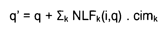
- crek ii + 1 crek ii - stsz ⁇ e ii + 1 ⁇ NLF k
- cimk ii + 1 cimk ii - stsz ⁇ e ii + 1 ⁇ NLF k in which stsz is a compression factor ( ⁇ 10 -7 ).
- the term within parentheses is proportional to the correlation between the error "e" at the time ii+1 and the NLF controlled by said coefficient and containing the i and q terms at the time ii+1; k varies from 1 to 10 as in the preceding example.
- Benedetto, Biglieri, Castellani in "Digital Transmission Theory” suggest analysing the channel to firsly reduce the number of NLFs to the necessary minimum in order to choose those which produce the most important effects, and then applying the MMSE criterion.
- the objective of controlling the transmitted spectrum regrowing along with the added noise within the baseband can be achieved only if the coefficient updating rate is the same as the transmission oversampling rate.
- the problem to be solved is therefore the method to calculate the error "e", which becomes the fundamental point.
- the chosen solution to calculate the error "e” is based on the transmitteddata and not on the decided data as is commonly done in the MMSE case.
- the error "e” is determined by the difference between the baseband signal which is to be transmitted (suitably delayed) and the signal received and demodulated (in baseband).
- Point c) relates to the fact that the non-linear block must be used under various different conditions related both to the variability of power to be transmitted, and to the variation of the peak/mean power ratio. These variations must be maintained satisfied by the single acquired measurement characterizing the non-linear block. At the discretion of the designer several measurements can be made if it is considered necessary to acquire different non-linear block characteristics due, for example, to variations in temperature or in other environmental conditions.
- the predistortion circuit consists of a block which executes the aforestated predistortion operation: the coefficients are extracted from a memory relative to the non-linear block in use and applied in accordance with the linearization formula, calculating the new predistorted modulating signals i' and q' from the original i and q signals.
- the modulating signals i' and q' corrected in this manner are then fed to the modulator to form the spectrum to be transmitted.
- the adaptive updating of the coefficients for their acquisition, at the preceding point a), involves a system which has to be implemented only during the production step, and which is described in the following block scheme.
- a system for linearizing microwave transmitters comprises a generator 10 for signals obtained from the data to be transmitted (the modulating signal), which is connected to an input port of a first adder node 11, the output of the adder node 11 being connected to a modulator 12 connected to a transmitter 13.
- a receiver 14 receives the signal transmitted by the transmitter 13.
- the output of the receiver 14 is connected to a block 15 which implements the receive equalizer function, recovers the carrier and locks the system synchronization clock.
- the signals generated by the generator 10 are also fed to a predistorter 16, the output of which is connected to the second input port of the adder 11. These signals are also fed to a delay block 17, the output of which is connected to a second adder 18 and possibly to a sampling and synchronisation block 19.
- the output of the receiver 14 is also connected to the sampling and synchronisation block 19.
- the predistorter 16 is connected to a memory 20 for storing the calculated predistortion coefficients.
- This circuit is to be set up during the testing stage for each non-linear device.
- the generator 10 generates the modulating signals in accordance with system requirements, including shaping filtering.
- the adder 11 adds to the modulating signals i and q the predistortion generated by the predistorter 16, in accordance with the preceding formula.
- the output signal from the adder node enters the modulator 12, the modulated carrier being transmitted by the non-linear block (transmitter 13) at the required maximum power for the device, and for which the required distortion conditions are to be satisfied.
- the signals are delayed by the delay block 17 and fed to the adder 18 and if necessary also to the block 19 to facilitate signal synchronization.
- the signal is returned to baseband by a receiver 14, demodulator, sampling and synchronisation block 19 in cascade.
- a wide band system as described can normally be prepared on a production bench.
- the demodulated signal is sampled at the same rate as the transmitted one.
- the block 19 synchronizes the delayed signals coming from the delay block 17 with the signals received by the receiver 14.
- the modulating samples are suitably delayed in order to be compared with their sampled version in reception.
- the adder 18 effects the difference between the signals at its input ports to provide an output indicative of the error between said two signals.
- the calculated difference error between the original and the received signals is used to apdate the coefficients.
- linear equalizer block 15 is suggested for recovering the synchronisms which are usefull for coherent demodulation of the signal transmitted by the transmitter 13.
- the coefficients are acquired, as already described, for the most severe peak/mean power ratio at which the non-linear block is operated.
- the maximum output power level on the curve hnl corresponds to the maximum allowable input level E on the horizontal axis : this is a physical limit which cannot be exceeded.
- the problem which now arises is that it may be required to modify the mean power level to be transmitted in the sense of reducing it, the previous operating point being relative to maximum power: this reduction requires the extent of the predistortion to be reduced.
- the signal at the input of the non-linear block can be varied, with a different but lower PP/MP ratio, having for example to vary the modulation order (reduced number of levels) and/or the rolloff value.
- the corresponding predistortion reduction is obtained by reducing the input power level to the predistortion block by X dB.
- the use of a new modulated signal (lower modulation order) characterized by a PP/MP ratio lower by X dB than the original characterization enables the same linearized distortion condition to be achieved, also increasing by X dB the output power from the transmitter.
- the new required degree of predistortion can be obtained by increasing the input power to the predistortion block by X dB: the designer should keep in mind that the peaks of the new signal must respect the aforedescribed maximum limit.
- the average power providable by the non-linear block can be utilized to its maximum extent.
- a multiplier could be applied before the predistortion block and a multiplier after the predistortion block to multiply the passing through signal with the previously determined coefficients.
- the log values (dB) of the coefficients vary by the same amount but are applied with opposite signs: if positive before the predistorter they become negative after the predistorter.
Landscapes
- Physics & Mathematics (AREA)
- Nonlinear Science (AREA)
- Engineering & Computer Science (AREA)
- Power Engineering (AREA)
- Amplifiers (AREA)
- Transmitters (AREA)
Claims (10)
- Système destiné à déterminer les coefficients de prédistorsion pour un émetteur à micro-ondes comprenant : une source de signal numérique (10) pour produire un signal numérique échantillonné ; un dispositif de prédistorsion (16) qui comprend un dispositif de calcul pour la distorsion dudit signal numérique ; et un émetteur (13) émettant ledit signal numérique distordu ; caractérisé en ce qu'il comprend un récepteur (14) pour recevoir ledit signal émis et fournir un signal échantillonné démodulé ; un dispositif de retard (17) pour retarder ledit signal numérique échantillonné ; un dispositif de comparaison (18) pour comparer ledit signal numérique échantillonné retardé au dit signal échantillonné démodulé pour produire un signal indiquant l'erreur entre lesdits deux signaux échantillonnés ; un dispositif de calcul (16) pour déterminer lesdits coefficients de prédistorsion sur la base dudit signal d'indication d'erreur ; et une mémoire (20) pour mémoriser lesdits coefficients de prédistorsion ; ledit dispositif de calcul (16) utilisant les formules suivantes :


où

dans lequel stsz est un facteur de compression < 10-7,
eii+1 est l'erreur entre lesdits deux signaux au moment ii+1,
NLFk est une fonction non linéaire d'indice k,
i et q sont des séquences de signaux échantillonnés,
i' et q' sont des séquences de signaux échantillonnés corrigés par la prédistorsion,
K est l'indice de l'ordre des fonctions non linéaires NLF(i, q) qui sont utilisées pour égaliser i et q et leur argument. - Système selon la revendication 1, caractérisé en ce que ledit signal numérique et ledit signal démodulé sont des signaux numériques en bande de base.
- Système selon la revendication 1, caractérisé en ce que ledit dispositif de prédistorsion (16) comprend un additionneur (11) pour ajouter au dit signal numérique un signal obtenu sur la base desdits coefficients de prédistorsion.
- Système selon la revendication 1, caractérisé en ce que ledit dispositif de retard (17) comprend un moyen pour synchroniser ledit signal numérique avec ledit signal démodulé.
- Système selon la revendication 1, caractérisé en ce que ledit émetteur (13) émet à la puissance maximale requise pour le dispositif.
- Procédé destiné à déterminer les coefficients de prédistorsion pour un émetteur à micro-ondes comprenant les étapes consistant à : générer un signal échantillonné numérique, opérer une prédistorsion dudit signal numérique, puis transmettre ledit signal numérique distordu ; caractérisé en ce qu'il comprend les étapes consistant à recevoir ledit signal transmis et à fournir un signal échantillonné démodulé, à retarder ledit signal numérique échantillonné, à comparer ledit signal numérique retardé au dit signal démodulé pour produire un signal indiquant l'erreur entre lesdits deux signaux, à déterminer lesdits coefficients de prédistorsion sur la base dudit signal d'indication d'erreur au cours de la production/du test de l'émetteur, et à mémoriser lesdits coefficients de prédistorsion ; lesdits coefficients de prédistorsion étant calculés au moyen des formules suivantes :

où

dans lequel stsz est un facteur de compression < 10-7,
eii+1 est l'erreur entre lesdits deux signaux au moment ii+1, NLFk est une fonction non linéaire d'indice k,
i et q sont des séquences de signaux échantillonnés,
i' et q' sont des séquences de signaux échantillonnés corrigés par la prédistorsion,
K est l'indice de l'ordre des fonctions non linéaires NLF(i, q) qui sont utilisées pour égaliser i et q et leur argument. - Procédé selon la revendication 6, caractérisé en ce que l'étape de prédistorsion comprend l'étape consistant à ajouter au dit signal numérique un signal obtenu sur la base desdits coefficients de prédistorsion.
- Procédé selon la revendication 6, caractérisé en ce que l'étape de retard comprend l'étape consistant à synchroniser ledit signal numérique avec ledit signal démodulé.
- Système pour linéariser des émetteurs à micro-ondes au cours d'un fonctionnement normal comprenant un dispositif de prédistorsion qui utilise les coefficients de prédistorsion déterminés selon la revendication 1.
- Système selon la revendication 1, caractérisé en ce que ledit émetteur émet à une puissance prédéterminée, une variation de ladite puissance prédéterminée engendrant une variation correspondante de la puissance d'entrée sur ledit dispositif de prédistorsion.
Priority Applications (3)
| Application Number | Priority Date | Filing Date | Title |
|---|---|---|---|
| EP07011316A EP2001127B1 (fr) | 2007-06-08 | 2007-06-08 | Système et procédé pour la linéarisation de transmetteurs à micro-ondes |
| ES07011316T ES2379994T3 (es) | 2007-06-08 | 2007-06-08 | Sistema y método para linealizar transmisiones de microondas |
| AT07011316T ATE541357T1 (de) | 2007-06-08 | 2007-06-08 | System und verfahren zur linearisierung von mikrowellensender |
Applications Claiming Priority (1)
| Application Number | Priority Date | Filing Date | Title |
|---|---|---|---|
| EP07011316A EP2001127B1 (fr) | 2007-06-08 | 2007-06-08 | Système et procédé pour la linéarisation de transmetteurs à micro-ondes |
Publications (2)
| Publication Number | Publication Date |
|---|---|
| EP2001127A1 EP2001127A1 (fr) | 2008-12-10 |
| EP2001127B1 true EP2001127B1 (fr) | 2012-01-11 |
Family
ID=38330017
Family Applications (1)
| Application Number | Title | Priority Date | Filing Date |
|---|---|---|---|
| EP07011316A Active EP2001127B1 (fr) | 2007-06-08 | 2007-06-08 | Système et procédé pour la linéarisation de transmetteurs à micro-ondes |
Country Status (3)
| Country | Link |
|---|---|
| EP (1) | EP2001127B1 (fr) |
| AT (1) | ATE541357T1 (fr) |
| ES (1) | ES2379994T3 (fr) |
Citations (1)
| Publication number | Priority date | Publication date | Assignee | Title |
|---|---|---|---|---|
| US20070129025A1 (en) * | 2005-12-01 | 2007-06-07 | Vasa John E | Open loop polar transmitter having on-chip calibration |
Family Cites Families (3)
| Publication number | Priority date | Publication date | Assignee | Title |
|---|---|---|---|---|
| JP4014343B2 (ja) * | 1999-12-28 | 2007-11-28 | 富士通株式会社 | 歪補償装置 |
| US7366252B2 (en) | 2004-01-21 | 2008-04-29 | Powerwave Technologies, Inc. | Wideband enhanced digital injection predistortion system and method |
| JP4308163B2 (ja) | 2005-03-22 | 2009-08-05 | 富士通株式会社 | 歪補償装置 |
-
2007
- 2007-06-08 ES ES07011316T patent/ES2379994T3/es active Active
- 2007-06-08 EP EP07011316A patent/EP2001127B1/fr active Active
- 2007-06-08 AT AT07011316T patent/ATE541357T1/de active
Patent Citations (1)
| Publication number | Priority date | Publication date | Assignee | Title |
|---|---|---|---|---|
| US20070129025A1 (en) * | 2005-12-01 | 2007-06-07 | Vasa John E | Open loop polar transmitter having on-chip calibration |
Also Published As
| Publication number | Publication date |
|---|---|
| ATE541357T1 (de) | 2012-01-15 |
| ES2379994T3 (es) | 2012-05-07 |
| EP2001127A1 (fr) | 2008-12-10 |
Similar Documents
| Publication | Publication Date | Title |
|---|---|---|
| US7330073B2 (en) | Arbitrary waveform predistortion table generation | |
| EP1723725B1 (fr) | Système de distorsion préalable numérique et procédé permettant de linéariser une amplification de puissance radioélectrique avec des caractéristiques de gains non linéaire et des effets de mémoire | |
| EP2443739B1 (fr) | Émetteur à haut rendement pour communication sans fil | |
| US8030997B2 (en) | Resource efficient adaptive digital pre-distortion system | |
| EP1800396B1 (fr) | Systeme et procede concernant la predistorsion de signaux | |
| EP2875620B1 (fr) | Procédé et système pour aligner des signaux largement espacés en fréquence pour une pré-distorsion numérique large bande dans des systèmes de communication sans fil | |
| EP1085668B1 (fr) | Un procédé et appareil pour reduire la puissance de canaux voisins dans des systèmes de communication sans-fil | |
| JP5251565B2 (ja) | プリディストータ及びその遅延調整方法 | |
| EP3416340A1 (fr) | Procédé et système de linéarisation de prédistorsion de bande de base dans des systèmes de communication large bande multicanaux | |
| US6630862B1 (en) | System for pre-distorting an input signal for a power amplifier using-non-orthogonal coordinates | |
| EP1450482B1 (fr) | Circuit et procédé pour la compensation des distorsions non-linéaires d'un amplificateur de puissance | |
| JP4863729B2 (ja) | 歪補償装置及び歪補償方法 | |
| EP1819040A1 (fr) | Dispositif pour la compensation des distorsions non-linéaires et méthode | |
| EP1932308B1 (fr) | Systeme amplificateur faisant appel a la predistorsion polynomiale analogique avec adaptation numerique sub-nyquist | |
| EP2001127B1 (fr) | Système et procédé pour la linéarisation de transmetteurs à micro-ondes | |
| US8538349B2 (en) | Method and device for pre-distorting an exciter and predistortion exciter | |
| WO2009011071A1 (fr) | Dispositif amplificateur avec compensation de distorsion non-linéaire | |
| US8324953B1 (en) | Method and a system for signal processing | |
| Binh et al. | The usability of distance degradation in estimation of signal to noise ratio degradation caused by the effect of nonlinear transmit amplifiers and optimum additional phase shift in 256-QAM systems | |
| JPH04292022A (ja) | 非線形歪補償器をもつディジタル無線装置 | |
| HK1066641A (en) | Circuit and method for compensating for nonliner distortion of power ampllifier |
Legal Events
| Date | Code | Title | Description |
|---|---|---|---|
| PUAI | Public reference made under article 153(3) epc to a published international application that has entered the european phase |
Free format text: ORIGINAL CODE: 0009012 |
|
| 17P | Request for examination filed |
Effective date: 20080325 |
|
| AK | Designated contracting states |
Kind code of ref document: A1 Designated state(s): AT BE BG CH CY CZ DE DK EE ES FI FR GB GR HU IE IS IT LI LT LU LV MC MT NL PL PT RO SE SI SK TR |
|
| AX | Request for extension of the european patent |
Extension state: AL BA HR MK RS |
|
| AKX | Designation fees paid |
Designated state(s): AT BE BG CH CY CZ DE DK EE ES FI FR GB GR HU IE IS IT LI LT LU LV MC MT NL PL PT RO SE SI SK TR |
|
| GRAP | Despatch of communication of intention to grant a patent |
Free format text: ORIGINAL CODE: EPIDOSNIGR1 |
|
| GRAS | Grant fee paid |
Free format text: ORIGINAL CODE: EPIDOSNIGR3 |
|
| GRAA | (expected) grant |
Free format text: ORIGINAL CODE: 0009210 |
|
| AK | Designated contracting states |
Kind code of ref document: B1 Designated state(s): AT BE BG CH CY CZ DE DK EE ES FI FR GB GR HU IE IS IT LI LT LU LV MC MT NL PL PT RO SE SI SK TR |
|
| REG | Reference to a national code |
Ref country code: GB Ref legal event code: FG4D |
|
| REG | Reference to a national code |
Ref country code: CH Ref legal event code: EP |
|
| REG | Reference to a national code |
Ref country code: AT Ref legal event code: REF Ref document number: 541357 Country of ref document: AT Kind code of ref document: T Effective date: 20120115 |
|
| REG | Reference to a national code |
Ref country code: IE Ref legal event code: FG4D |
|
| REG | Reference to a national code |
Ref country code: DE Ref legal event code: R096 Ref document number: 602007019907 Country of ref document: DE Effective date: 20120315 |
|
| REG | Reference to a national code |
Ref country code: NL Ref legal event code: VDEP Effective date: 20120111 |
|
| REG | Reference to a national code |
Ref country code: ES Ref legal event code: FG2A Ref document number: 2379994 Country of ref document: ES Kind code of ref document: T3 Effective date: 20120507 |
|
| PG25 | Lapsed in a contracting state [announced via postgrant information from national office to epo] |
Ref country code: SI Free format text: LAPSE BECAUSE OF FAILURE TO SUBMIT A TRANSLATION OF THE DESCRIPTION OR TO PAY THE FEE WITHIN THE PRESCRIBED TIME-LIMIT Effective date: 20120111 |
|
| LTIE | Lt: invalidation of european patent or patent extension |
Effective date: 20120111 |
|
| PG25 | Lapsed in a contracting state [announced via postgrant information from national office to epo] |
Ref country code: BE Free format text: LAPSE BECAUSE OF FAILURE TO SUBMIT A TRANSLATION OF THE DESCRIPTION OR TO PAY THE FEE WITHIN THE PRESCRIBED TIME-LIMIT Effective date: 20120111 Ref country code: NL Free format text: LAPSE BECAUSE OF FAILURE TO SUBMIT A TRANSLATION OF THE DESCRIPTION OR TO PAY THE FEE WITHIN THE PRESCRIBED TIME-LIMIT Effective date: 20120111 Ref country code: LT Free format text: LAPSE BECAUSE OF FAILURE TO SUBMIT A TRANSLATION OF THE DESCRIPTION OR TO PAY THE FEE WITHIN THE PRESCRIBED TIME-LIMIT Effective date: 20120111 Ref country code: BG Free format text: LAPSE BECAUSE OF FAILURE TO SUBMIT A TRANSLATION OF THE DESCRIPTION OR TO PAY THE FEE WITHIN THE PRESCRIBED TIME-LIMIT Effective date: 20120411 Ref country code: IS Free format text: LAPSE BECAUSE OF FAILURE TO SUBMIT A TRANSLATION OF THE DESCRIPTION OR TO PAY THE FEE WITHIN THE PRESCRIBED TIME-LIMIT Effective date: 20120511 |
|
| PG25 | Lapsed in a contracting state [announced via postgrant information from national office to epo] |
Ref country code: PT Free format text: LAPSE BECAUSE OF FAILURE TO SUBMIT A TRANSLATION OF THE DESCRIPTION OR TO PAY THE FEE WITHIN THE PRESCRIBED TIME-LIMIT Effective date: 20120511 Ref country code: PL Free format text: LAPSE BECAUSE OF FAILURE TO SUBMIT A TRANSLATION OF THE DESCRIPTION OR TO PAY THE FEE WITHIN THE PRESCRIBED TIME-LIMIT Effective date: 20120111 Ref country code: FI Free format text: LAPSE BECAUSE OF FAILURE TO SUBMIT A TRANSLATION OF THE DESCRIPTION OR TO PAY THE FEE WITHIN THE PRESCRIBED TIME-LIMIT Effective date: 20120111 Ref country code: LV Free format text: LAPSE BECAUSE OF FAILURE TO SUBMIT A TRANSLATION OF THE DESCRIPTION OR TO PAY THE FEE WITHIN THE PRESCRIBED TIME-LIMIT Effective date: 20120111 Ref country code: GR Free format text: LAPSE BECAUSE OF FAILURE TO SUBMIT A TRANSLATION OF THE DESCRIPTION OR TO PAY THE FEE WITHIN THE PRESCRIBED TIME-LIMIT Effective date: 20120412 |
|
| REG | Reference to a national code |
Ref country code: AT Ref legal event code: MK05 Ref document number: 541357 Country of ref document: AT Kind code of ref document: T Effective date: 20120111 |
|
| PG25 | Lapsed in a contracting state [announced via postgrant information from national office to epo] |
Ref country code: CY Free format text: LAPSE BECAUSE OF FAILURE TO SUBMIT A TRANSLATION OF THE DESCRIPTION OR TO PAY THE FEE WITHIN THE PRESCRIBED TIME-LIMIT Effective date: 20120111 |
|
| PG25 | Lapsed in a contracting state [announced via postgrant information from national office to epo] |
Ref country code: RO Free format text: LAPSE BECAUSE OF FAILURE TO SUBMIT A TRANSLATION OF THE DESCRIPTION OR TO PAY THE FEE WITHIN THE PRESCRIBED TIME-LIMIT Effective date: 20120111 Ref country code: DK Free format text: LAPSE BECAUSE OF FAILURE TO SUBMIT A TRANSLATION OF THE DESCRIPTION OR TO PAY THE FEE WITHIN THE PRESCRIBED TIME-LIMIT Effective date: 20120111 Ref country code: CZ Free format text: LAPSE BECAUSE OF FAILURE TO SUBMIT A TRANSLATION OF THE DESCRIPTION OR TO PAY THE FEE WITHIN THE PRESCRIBED TIME-LIMIT Effective date: 20120111 Ref country code: EE Free format text: LAPSE BECAUSE OF FAILURE TO SUBMIT A TRANSLATION OF THE DESCRIPTION OR TO PAY THE FEE WITHIN THE PRESCRIBED TIME-LIMIT Effective date: 20120111 Ref country code: SE Free format text: LAPSE BECAUSE OF FAILURE TO SUBMIT A TRANSLATION OF THE DESCRIPTION OR TO PAY THE FEE WITHIN THE PRESCRIBED TIME-LIMIT Effective date: 20120111 |
|
| PLBE | No opposition filed within time limit |
Free format text: ORIGINAL CODE: 0009261 |
|
| STAA | Information on the status of an ep patent application or granted ep patent |
Free format text: STATUS: NO OPPOSITION FILED WITHIN TIME LIMIT |
|
| PG25 | Lapsed in a contracting state [announced via postgrant information from national office to epo] |
Ref country code: SK Free format text: LAPSE BECAUSE OF FAILURE TO SUBMIT A TRANSLATION OF THE DESCRIPTION OR TO PAY THE FEE WITHIN THE PRESCRIBED TIME-LIMIT Effective date: 20120111 |
|
| 26N | No opposition filed |
Effective date: 20121012 |
|
| PG25 | Lapsed in a contracting state [announced via postgrant information from national office to epo] |
Ref country code: AT Free format text: LAPSE BECAUSE OF FAILURE TO SUBMIT A TRANSLATION OF THE DESCRIPTION OR TO PAY THE FEE WITHIN THE PRESCRIBED TIME-LIMIT Effective date: 20120111 Ref country code: MC Free format text: LAPSE BECAUSE OF NON-PAYMENT OF DUE FEES Effective date: 20120630 |
|
| REG | Reference to a national code |
Ref country code: CH Ref legal event code: PL |
|
| REG | Reference to a national code |
Ref country code: DE Ref legal event code: R097 Ref document number: 602007019907 Country of ref document: DE Effective date: 20121012 |
|
| REG | Reference to a national code |
Ref country code: CH Ref legal event code: PL |
|
| REG | Reference to a national code |
Ref country code: IE Ref legal event code: MM4A |
|
| PG25 | Lapsed in a contracting state [announced via postgrant information from national office to epo] |
Ref country code: LI Free format text: LAPSE BECAUSE OF NON-PAYMENT OF DUE FEES Effective date: 20120630 Ref country code: IE Free format text: LAPSE BECAUSE OF NON-PAYMENT OF DUE FEES Effective date: 20120608 Ref country code: CH Free format text: LAPSE BECAUSE OF NON-PAYMENT OF DUE FEES Effective date: 20120630 |
|
| PG25 | Lapsed in a contracting state [announced via postgrant information from national office to epo] |
Ref country code: MT Free format text: LAPSE BECAUSE OF FAILURE TO SUBMIT A TRANSLATION OF THE DESCRIPTION OR TO PAY THE FEE WITHIN THE PRESCRIBED TIME-LIMIT Effective date: 20120111 |
|
| PG25 | Lapsed in a contracting state [announced via postgrant information from national office to epo] |
Ref country code: TR Free format text: LAPSE BECAUSE OF FAILURE TO SUBMIT A TRANSLATION OF THE DESCRIPTION OR TO PAY THE FEE WITHIN THE PRESCRIBED TIME-LIMIT Effective date: 20120111 |
|
| PG25 | Lapsed in a contracting state [announced via postgrant information from national office to epo] |
Ref country code: LU Free format text: LAPSE BECAUSE OF NON-PAYMENT OF DUE FEES Effective date: 20120608 |
|
| PG25 | Lapsed in a contracting state [announced via postgrant information from national office to epo] |
Ref country code: HU Free format text: LAPSE BECAUSE OF FAILURE TO SUBMIT A TRANSLATION OF THE DESCRIPTION OR TO PAY THE FEE WITHIN THE PRESCRIBED TIME-LIMIT Effective date: 20070608 |
|
| REG | Reference to a national code |
Ref country code: FR Ref legal event code: PLFP Year of fee payment: 10 |
|
| REG | Reference to a national code |
Ref country code: FR Ref legal event code: PLFP Year of fee payment: 11 |
|
| REG | Reference to a national code |
Ref country code: FR Ref legal event code: PLFP Year of fee payment: 12 |
|
| PGFP | Annual fee paid to national office [announced via postgrant information from national office to epo] |
Ref country code: DE Payment date: 20180625 Year of fee payment: 12 |
|
| REG | Reference to a national code |
Ref country code: DE Ref legal event code: R119 Ref document number: 602007019907 Country of ref document: DE |
|
| PG25 | Lapsed in a contracting state [announced via postgrant information from national office to epo] |
Ref country code: DE Free format text: LAPSE BECAUSE OF NON-PAYMENT OF DUE FEES Effective date: 20200101 |
|
| PGFP | Annual fee paid to national office [announced via postgrant information from national office to epo] |
Ref country code: GB Payment date: 20200629 Year of fee payment: 14 |
|
| PGFP | Annual fee paid to national office [announced via postgrant information from national office to epo] |
Ref country code: ES Payment date: 20200701 Year of fee payment: 14 |
|
| PGFP | Annual fee paid to national office [announced via postgrant information from national office to epo] |
Ref country code: FR Payment date: 20210625 Year of fee payment: 15 |
|
| GBPC | Gb: european patent ceased through non-payment of renewal fee |
Effective date: 20210608 |
|
| PG25 | Lapsed in a contracting state [announced via postgrant information from national office to epo] |
Ref country code: GB Free format text: LAPSE BECAUSE OF NON-PAYMENT OF DUE FEES Effective date: 20210608 |
|
| REG | Reference to a national code |
Ref country code: ES Ref legal event code: FD2A Effective date: 20220805 |
|
| PG25 | Lapsed in a contracting state [announced via postgrant information from national office to epo] |
Ref country code: ES Free format text: LAPSE BECAUSE OF NON-PAYMENT OF DUE FEES Effective date: 20210609 |
|
| PG25 | Lapsed in a contracting state [announced via postgrant information from national office to epo] |
Ref country code: FR Free format text: LAPSE BECAUSE OF NON-PAYMENT OF DUE FEES Effective date: 20220630 |
|
| PGFP | Annual fee paid to national office [announced via postgrant information from national office to epo] |
Ref country code: IT Payment date: 20250826 Year of fee payment: 19 |