EP2003695A2 - Dünnfilmtransistor, Verfahren zur Herstellung des Dünnfilmtransistors und Anzeigegerät mit dem Dünnfilmtransistor - Google Patents
Dünnfilmtransistor, Verfahren zur Herstellung des Dünnfilmtransistors und Anzeigegerät mit dem Dünnfilmtransistor Download PDFInfo
- Publication number
- EP2003695A2 EP2003695A2 EP08252041A EP08252041A EP2003695A2 EP 2003695 A2 EP2003695 A2 EP 2003695A2 EP 08252041 A EP08252041 A EP 08252041A EP 08252041 A EP08252041 A EP 08252041A EP 2003695 A2 EP2003695 A2 EP 2003695A2
- Authority
- EP
- European Patent Office
- Prior art keywords
- metal
- layer
- semiconductor layer
- crystallization
- channel region
- Prior art date
- Legal status (The legal status is an assumption and is not a legal conclusion. Google has not performed a legal analysis and makes no representation as to the accuracy of the status listed.)
- Withdrawn
Links
Images


Classifications
-
- H—ELECTRICITY
- H10—SEMICONDUCTOR DEVICES; ELECTRIC SOLID-STATE DEVICES NOT OTHERWISE PROVIDED FOR
- H10D—INORGANIC ELECTRIC SEMICONDUCTOR DEVICES
- H10D30/00—Field-effect transistors [FET]
- H10D30/60—Insulated-gate field-effect transistors [IGFET]
- H10D30/67—Thin-film transistors [TFT]
- H10D30/6704—Thin-film transistors [TFT] having supplementary regions or layers in the thin films or in the insulated bulk substrates for controlling properties of the device
- H10D30/6706—Thin-film transistors [TFT] having supplementary regions or layers in the thin films or in the insulated bulk substrates for controlling properties of the device for preventing leakage current
-
- H—ELECTRICITY
- H10—SEMICONDUCTOR DEVICES; ELECTRIC SOLID-STATE DEVICES NOT OTHERWISE PROVIDED FOR
- H10D—INORGANIC ELECTRIC SEMICONDUCTOR DEVICES
- H10D30/00—Field-effect transistors [FET]
- H10D30/60—Insulated-gate field-effect transistors [IGFET]
- H10D30/67—Thin-film transistors [TFT]
- H10D30/6757—Thin-film transistors [TFT] characterised by the structure of the channel, e.g. transverse or longitudinal shape or doping profile
-
- H—ELECTRICITY
- H10—SEMICONDUCTOR DEVICES; ELECTRIC SOLID-STATE DEVICES NOT OTHERWISE PROVIDED FOR
- H10D—INORGANIC ELECTRIC SEMICONDUCTOR DEVICES
- H10D86/00—Integrated devices formed in or on insulating or conducting substrates, e.g. formed in silicon-on-insulator [SOI] substrates or on stainless steel or glass substrates
- H10D86/01—Manufacture or treatment
- H10D86/021—Manufacture or treatment of multiple TFTs
- H10D86/0221—Manufacture or treatment of multiple TFTs comprising manufacture, treatment or patterning of TFT semiconductor bodies
- H10D86/0223—Manufacture or treatment of multiple TFTs comprising manufacture, treatment or patterning of TFT semiconductor bodies comprising crystallisation of amorphous, microcrystalline or polycrystalline semiconductor materials
- H10D86/0225—Manufacture or treatment of multiple TFTs comprising manufacture, treatment or patterning of TFT semiconductor bodies comprising crystallisation of amorphous, microcrystalline or polycrystalline semiconductor materials using crystallisation-promoting species, e.g. using a Ni catalyst
-
- H—ELECTRICITY
- H10—SEMICONDUCTOR DEVICES; ELECTRIC SOLID-STATE DEVICES NOT OTHERWISE PROVIDED FOR
- H10D—INORGANIC ELECTRIC SEMICONDUCTOR DEVICES
- H10D86/00—Integrated devices formed in or on insulating or conducting substrates, e.g. formed in silicon-on-insulator [SOI] substrates or on stainless steel or glass substrates
- H10D86/40—Integrated devices formed in or on insulating or conducting substrates, e.g. formed in silicon-on-insulator [SOI] substrates or on stainless steel or glass substrates characterised by multiple TFTs
- H10D86/60—Integrated devices formed in or on insulating or conducting substrates, e.g. formed in silicon-on-insulator [SOI] substrates or on stainless steel or glass substrates characterised by multiple TFTs wherein the TFTs are in active matrices
-
- H—ELECTRICITY
- H10—SEMICONDUCTOR DEVICES; ELECTRIC SOLID-STATE DEVICES NOT OTHERWISE PROVIDED FOR
- H10P—GENERIC PROCESSES OR APPARATUS FOR THE MANUFACTURE OR TREATMENT OF DEVICES COVERED BY CLASS H10
- H10P14/00—Formation of materials, e.g. in the shape of layers or pillars
- H10P14/20—Formation of materials, e.g. in the shape of layers or pillars of semiconductor materials
- H10P14/32—Formation of materials, e.g. in the shape of layers or pillars of semiconductor materials characterised by intermediate layers between substrates and deposited layers
- H10P14/3202—Materials thereof
- H10P14/3238—Materials thereof being insulating materials
-
- H—ELECTRICITY
- H10—SEMICONDUCTOR DEVICES; ELECTRIC SOLID-STATE DEVICES NOT OTHERWISE PROVIDED FOR
- H10P—GENERIC PROCESSES OR APPARATUS FOR THE MANUFACTURE OR TREATMENT OF DEVICES COVERED BY CLASS H10
- H10P14/00—Formation of materials, e.g. in the shape of layers or pillars
- H10P14/20—Formation of materials, e.g. in the shape of layers or pillars of semiconductor materials
- H10P14/34—Deposited materials, e.g. layers
- H10P14/3402—Deposited materials, e.g. layers characterised by the chemical composition
- H10P14/3404—Deposited materials, e.g. layers characterised by the chemical composition being Group IVA materials
- H10P14/3411—Silicon, silicon germanium or germanium
-
- H—ELECTRICITY
- H10—SEMICONDUCTOR DEVICES; ELECTRIC SOLID-STATE DEVICES NOT OTHERWISE PROVIDED FOR
- H10P—GENERIC PROCESSES OR APPARATUS FOR THE MANUFACTURE OR TREATMENT OF DEVICES COVERED BY CLASS H10
- H10P14/00—Formation of materials, e.g. in the shape of layers or pillars
- H10P14/20—Formation of materials, e.g. in the shape of layers or pillars of semiconductor materials
- H10P14/38—Formation of materials, e.g. in the shape of layers or pillars of semiconductor materials characterised by treatments done after the formation of the materials
- H10P14/3802—Crystallisation or recrystallisation of non-monocrystalline semiconductor materials, e.g. regrowth
- H10P14/3806—Crystallisation or recrystallisation of non-monocrystalline semiconductor materials, e.g. regrowth using crystallisation-enhancing elements
Definitions
- TFT thin film transistor
- TFTs thin film transistors
- AMLCDs active matrix liquid crystal displays
- OLED organic light emitting diode
- a leakage current is proportional to the width of a channel region and inversely proportional to the length of the channel region.
- the length of the channel region is increased in order to reduce the leakage current, it is difficult to produce the intended effect.
- the size of the display device also increases and an aperture ratio decreases. Therefore, there is a specific technical limit to increase the length of the channel region.
- a crystallization technique using a crystallization-inducing metal for example a metal induced crystallization (MIC) technique, a metal induced lateral crystallization(MILC) technique and a super grain silicon(SGS) technique, because the techniques may crystallize an amorphous silicon (a-Si) layer at a lower temperature in a shorter amount of time than a solid-phase crystallization (SPC) technique or an excimer laser annealing (ELA) technique.
- MIC metal induced crystallization
- MILC metal induced lateral crystallization
- SGS super grain silicon
- a leakage current of the TFT varies irrespective of the length or width of a channel region unlike in typical TFTs.
- aspects of the present invention provide a thin film transistor (TFT) using a semiconductor layer crystallized using a crystallization-inducing metal, a method of fabricating the TFT, and a display device including the TFT.
- TFT thin film transistor
- a leakage current may be reduced by eliminating a crystallization-inducing metal from a channel region of the semiconductor layer.
- a leakage current may be predicted according to the width and length of the channel region of the semiconductor layer. Conversely, the width and length of the channel region of the semiconductor layer may be determined considering a leakage current to be controlled.
- a thin film transistor comprising: a semiconductor layer having source and drain regions and a channel region from which a crystallization-inducing metal has been gettered, and the semiconductor layer having a predetermined leakage current determined according to a length and a width of the channel region.
- a thin film transistor comprising: a semiconductor layer having source and drain regions and a channel region from which a crystallization-inducing metal has been gettered, and the semiconductor layer having a predetermined length and a predetermined width determined according to a leakage current of the semiconductor layer.
- a method of fabricating a thin film transistor comprising: crystallizing an amorphous silicon (a-Si) layer into a polycrystalline silicon (poly-Si) layer using a crystallization-inducing metal; determining a length and a width of a channel region of a semiconductor layer according to a predetermined leakage current; patterning the poly-Si layer to form the semiconductor layer having the channel region with the determined length and determined width; and gettering the crystallization-inducing metal from the channel region with a metal other than the crystallization-inducing metal or a silicide of a metal other than the crystallization metal.
- a method of fabricating a thin film transistor comprising: crystallizing an amorphous silicon (a-Si) layer into a polycrystalline silicon (poiy-Si) layer using a crystallization-inducing metal; determining a length of a channel region of a semiconductor layer according to a predetermined width and a predetermined leakage current: patterning the poly-Si layer to form the semiconductor layer having the channel region with the determined length and determined width; and gettering the crystallization-inducing metal from the channel region with a metal other than the crystallization-inducing metal or a silicide of a metal other than the crystallization metal.
- a method of fabricating a thin film transistor comprising crystallizing an amorphous silicon (a-Si) layer into a polycrystalline silicon (poly-Si) layer using a crystallization-inducing metal; determining a width of a channel region of a semiconductor layer according to a predetermined length and a predetermined leakage current: patterning the poly-Si layer to form the semiconductor layer having the channel region with the determined length and determined width; and gettering the crystallization-inducing metal from the channel region with a metal other than the crystallization-inducing metal or a silicide of a metal other than the crystallization metal.
- FIG. 1 is a cross-sectional view of a thin film transistor (TFT) according to an embodiment of the present invention
- FIG. 2 is a cross-sectional view of a semiconductor layer of the TFT shown in FIG. 1 .
- TFT thin film transistor
- a substrate 100 is provided.
- the substrate 100 may be a glass as shown in this embodiment substrate or a plastic substrate.
- a buffer layer 105 may be disposed on the substrate 100.
- the buffer layer 105 may prevent diffusion of moisture or impurities generated in the substrate 100 or control the transmission rate of heat during a crystallization process so as to facilitate the crystallization of an amorphous silicon (a-Si) layer.
- the buffer layer 105 may be formed of a single or multiple-layer insulating layer, such as a silicon oxide layer or a silicon nitride layer.
- a patterned semiconductor layer 135 is disposed on the buffer layer 105.
- the semiconductor layer 135 may be obtained through a crystallization technique using a crystallization-inducing metal such as a metal induced crystallization (MIC) technique, a metal induced lateral crystallization (MILC) technique, or a super grain silicon (SGS) technique.
- the semiconductor layer 135 includes a channel region 136 and source and drain regions 137 and 138.
- the SGS technique is more appropriate than the MIC technique or the MILC technique in forming the semiconductor layer 135 because the SGS technique may retain a low concentration of a crystallization-inducing metal.
- a channel region 136 of the semiconductor layer 135 has a length L and a width W.
- the length L of the channel region 136 corresponds to a distance between the source and drain regions 137 and 138 of the semiconductor layer 135, and the width W of the channel region 136 corresponds to a width of the channel region 136 perpendicular to the distance between the source and drain regions 137 and 138.
- the length L( ⁇ m) of the channel region 136 of the semiconductor layer 135 and a leakage current loff(A) per 1 mm of the width W of the channel region 136 of the semiconductor layer 135, i.e., the leakage current loff/W as a function of the length L, can be expressed as in Equation 1:
- Equation 1 since a leakage current may be predicted according to the size of the channel region 136 of the semiconductor layer 135, the leakage current may be controlled using the width W or length L of the channel region 136 of the semiconductor layer 135. Conversely, since the leakage current may be predicted, the length L or width W of the channel region 136 of the semiconductor layer 135 may be determined considering a leakage current to be controlled.
- a leakage current per 1 mm of the width W of the channel region 136 also decreases because of the more efficient removal of the crystallization-inducing metal from the channel region 136 using a region where either a metal other than the crystallization-inducing metal or a metal silicide thereof is formed.
- a value loff/W may be 1.0x10 -12 A or less due to a high gettering effect, so that the TFT can exhibit good characteristics in a display device.
- a region 145a in which either a metal, the metal being other than the crystallization-inducing metal or a metal silicide thereof is formed is disposed in the semiconductor layer 135 to a predetermined depth from a surface of the semiconductor layer 135 and spaced apart from the channel region 136.
- the metal or the metal silicide is used for the gettering process.
- the gettering process is performed using the region 145a in which the metal or the metal silicide is formed, thereby removing the crystallization-inducing metal from the channel region 136 of the semiconductor layer 135.
- a leakage current may be reduced and the length L( ⁇ m) of the channel region 136 of the semiconductor layer 135 and the leakage current loff/W(A/mm) per 1 mm of the width W of the channel region 136 of the semiconductor layer 135 may satisfy Equation 1.
- a distance between the channel region 136 and the region 145a in which either the metal other than the crystallization-inducing metal or the metal silicide thereof is formed may be constant irrespective of the length L of the channel region 136.
- the length L of the channel region 136 may vary, and the distance between the channel region 136 and the region 145a may be constant with respect to the length L of the channel region 136.
- the metal or metal silicide used for the gettering process may have a lower diffusion coefficient than the crystallization-inducing metal in the semiconductor layer 135.
- the diffusion coefficient of the metal or metal silicide used for the gettering process may be 1% or less of the diffusion coefficient of the crystallization-inducing metal in the semiconductor layer 135.
- the metal or metal silicide used for the gettering process may be prevented from diffusing from the region 145a into the remaining region of the semiconductor layer 135.
- Ni nickel
- Ni has a diffusion coefficient of about 10 -5 cm 2 /s or less in the semiconductor layer 135. Therefore, when Ni is used as the crystallization-inducing metal, the diffusion coefficient of the metal or metal silicide used for the gettering process may be 1% or less of the diffusion coefficient of Ni. Specifically, the metal or metal silicide may have a diffusion coefficient of 10 -7 cm 2 /s or less.
- the metal or metal silicide used for the gettering process may be one selected from the group consisting of Sc, Ti, Zr, Hf, V, Nb, Ta, Cr, Mo, W, Mn, Re, Ru, Os, Co, Rh, Ir, Pt, Y, La, Ce, Pr, Nd, Dy, Ho, TiN, TaN, alloys thereof, and metal silicides thereof.
- a gate insulating layer 150 is disposed on the surface of the substrate 100 including the semiconductor layer 135.
- the gate insulating layer 150 may be a silicon oxide layer, a silicon nitride layer, or a double layer thereof.
- a gate electrode 155 is disposed on a region of the gate insulating layer 150 corresponding to the channel region 136 of the semiconductor layer 135.
- the gate electrode 155 may be a single layer formed of aluminum (Al) or an Al alloy, such as aluminum-neodymium (Al-Nd), or a multiple layer obtained by stacking an Al alloy layer on a chromium (Cr) alloy layer or a molybdenum (Mo) alloy layer.
- An interlayer insulating layer 160 is disposed on the surface of the substrate 100 including the gate electrode 155.
- the interlayer insulating layer 160 may be a silicon nitride layer, a silicon oxide layer, or include multiple layers thereof.
- Source and drain electrodes 167 and 168 are disposed on the interlayer insulating layer 160 and electrically connected to the source and drain regions 137 and 138, respectively, of the semiconductor layer 135. Thus, the TFT according to the present embodiment is completed.
- the metal or metal silicide may comprise the same material as the gate electrode 155 or the source and drain electrodes 167 and 168.
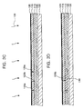
- FIGS. 3A through 3G are cross-sectional views illustrating a process of fabricating the TFT shown in FIG. 1 .
- a buffer layer 105 is formed on a substrate 100 formed of glass, stainless steel, or plastic.
- the buffer layer 105 may be a single layer or a multiple layer obtained by depositing an insulating layer, such as a silicon oxide layer or a silicon nitride layer, using a chemical vapor deposition (CVD) technique or a physical vapor deposition (PVD) technique.
- CVD chemical vapor deposition
- PVD physical vapor deposition
- the buffer layer 105 may prevent diffusion of moisture or impurities generated in the substrate 100 or control the transmission rate of heat during a crystallization process so as to facilitate crystallization of an amorphous silicon (a-Si) layer.
- a-Si amorphous silicon
- an a-Si layer 110 is formed on the buffer layer 105.
- the a-Si layer 110 may be formed using a CVD technique or a PVD technique.
- a dehydrogenation process may be performed during or after the formation of the a-Si layer 110, thereby lowering the concentration of hydrogen therein.
- the a-Si layer 110 is crystallized into a polycrystalline silicon (poly-Si) layer 130 (of FIG. 3D ).
- the crystallization of the a-Si layer 110 into the poly-Si layer 130 may be performed by a method using a crystallization-inducing metal, such as a metal induced crystallization (MIC) technique, a metal induced lateral crystallization (MILC) technique, or a super grain silicon (SGS) technique.
- MIC metal induced crystallization
- MILC metal induced lateral crystallization
- SGS super grain silicon
- a crystallization-inducing metal such as nickel (Ni), palladium (Pd), or aluminum (Al)
- Ni nickel
- Pd palladium
- Al aluminum
- metal silicide obtained by a reaction between a crystallization-inducing metal and silicon continuously diffuses in a lateral direction so that the a-Si layer 110 is crystallized into a poly-Si layer 130 by sequentially inducing crystallization of the silicon in the a-Si layer 110.
- the SGS technique maintains a lower concentration of a crystallization-inducing metal diffusing into the a-Si layer 110 than in the MIC technique or the MILC technique, so that crystal grains may be controlled to be in the range of several ⁇ m to several hundred ⁇ m.
- a capping layer 115 (of FIG. 3B ) may be formed on the a-Si layer 110, and a crystallization-inducing metal layer may be formed on the capping layer and annealed so as to diffuse a crystallization-inducing metal.
- the capping layer 115 may be omitted and a low-concentration crystallization-inducing metal layer may be formed so that the concentration of a crystallization-inducing metal diffusing into the a-Si layer 110 may be reduced.
- FIG. 3B is a cross-sectional view of a process of forming the capping layer 115 and a crystallization-inducing metal on the a-Si layer 110.
- the capping layer 115 is formed on the a-Si layer 110.
- the capping layer 115 may be a silicon nitride layer, in which case it is easy to control diffusion of a subsequently formed crystallization-inducing metal during an annealing process.
- the capping layer 115 may be a double layer of a silicon nitride layer and a silicon oxide layer.
- the capping layer 115 may be formed using a CVD technique or a PVD technique. In this case, the capping layer 115 may be formed to a thickness of about 0.1 to 200 nm. When the capping layer 115 is less than 0.1 nm, the capping layer 115 may not control the amount of the crystallization-inducing metal diffusing into the a-Si layer 110. When the capping layer 115 is greater than 200 nm, only a small amount of the crystallization-inducing metal diffuses into the a-Si layer 110, thereby precluding crystallization of the a-Si layer 110 into a poly-Si layer 130.
- a crystallization-inducing metal is deposited on the capping layer 115, thereby forming a crystallization-inducing metal layer 120.
- the crystallization-inducing metal may be one selected from the group consisting of Ni, Pd, Ag, Au, Al, Sn, Sb, Cu, Tb, and Cd. Ni may be preferred as the crystallization-inducing metal.
- the crystallization-inducing metal layer 120 may be formed to an areal density of 10 11 to 10 15 atoms/cm 2 on the capping layer 115.
- the crystallization-inducing metal layer 120 When the crystallization-inducing metal layer 120 is formed to an areal density lower than 10 11 to 10 15 atoms/cm 2 , it is difficult to crystallize the a-Si layer 110 into a poly-Si layer due to the small number of crystallization nuclei (i.e., seeds). Conversely, when the crystallization-inducing metal layer 120 is formed to an areal density higher than 10 11 to 10 15 atoms/cm 2 , an excessively large amount of the crystallization-inducing metal diffuses into the a-Si layer 110, thereby reducing the size of crystal grains of a poly-Si layer and increasing the amount of the remaining crystallization-inducing metal. As a result, a semiconductor layer obtained by patterning the poly-Si layer may have degraded characteristics.
- FIG. 3C is a cross-sectional view of a process of annealing the substrate 100 to diffuse the crystallization-inducing metal via the capping layer 115 to an interface between the capping layer 115 and the a-Si layer 110.
- the substrate 100 on which the buffer layer 105, the a-Si layer 110, the capping layer 115, and the crystallization-inducing metal layer 120 are formed is annealed (as indicated by reference numeral 125) so as to diffuse part of the crystallization-inducing metal of the crystallization-inducing metal layer 120 into the surface of the a-Si layer 110.
- the amount of the crystallization-inducing metal 120b that reaches the surface of the a-Si layer 110 depends on the diffusion barrier capability of the capping layer 115, which is closely associated with the thickness and density of the capping layer 115. Specifically, as the thickness or density of the capping layer 115 increases, the amount of the crystallization-inducing metal 120b that diffuses into the a-Si layer 110 decreases, and thus the size of crystal grains of a poly-Si layer 130 increases. Conversely, as the thickness or density of the capping layer 115 decreases, the amount of the crystallization-inducing metal 120b that diffuses into the a-Si layer 110 increases, and thus the size of the crystal grains of the poly-Si layer 130 decreases.
- the annealing process for diffusing the crystallization-inducing metal is performed at a temperature of about 200 to 900°C for several seconds to several hours in consideration of the fabrication cost and yield.
- the annealing process may be one of a furnace process, a rapid thermal annealing (RTA) process, an ultraviolet (UV) process, and a laser process.
- FIG. 3D is a cross-sectional view of a process of crystallizing the a-Si layer 110 into a poly-Si layer 130 due to the diffused crystallization-inducing metal.
- the a-Si layer 110 is crystallized into the poly-Si layer 130 due to the crystallization-inducing metal 120b that passes through the capping layer 115 and diffuses into the surface of the a-Si layer 110.
- the diffused crystallization-inducing metal 120b combines with silicon (Si) of the a-Si layer 110 to form metal silicide as crystallization nuclei (i.e., seeds).
- the a-Si layer 110 is crystallized into the poly-Si layer 130 using the seeds.
- FIG. 3D illustrates that the annealing process is performed on the resultant structure from which the capping layer 115 and the crystallization-inducing metal layer 120 are not removed
- aspects of the present invention is not limited thereto. That is, after the crystallization-inducing metal is diffused into the a-Si layer 110 to form metal silicide, the capping layer 115 and the crystallization-inducing metal layer 120 may be removed and the resultant structure may be annealed to form the poly-Si layer 130.
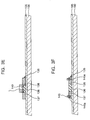
- the capping layer 115 and the crystallization-inducing metal layer 120 are removed, and the poly-Si layer 130 is patterned to form a semiconductor layer 135. Unlike in the present embodiment, the poly-Si layer 130 may be patterned during a subsequent process.
- a length and width of the semiconductor layer 135 are determined in consideration of Equation 1:
- a length L and a width W of a channel region 136 of the semiconductor layer 135 are determined according to a leakage current to be controlled, and the length and width of the semiconductor layer 135 are determined in consideration of the length L and width W of the channel region 136.
- a leakage current per 1 mm of the width W of the channel region also decreases because of more efficient removal of the crystallization-inducing metal from the channel region using a subsequent metal layer or metal silicide layer used for a gettering process.
- a value loff/W can be 1.0x10 -12 A or less due to a high gettering effect so that the resultant TFT can exhibit good characteristics as a display device.
- a photoresist pattern 140 is formed on a region of the semiconductor layer 135 where a channel region 136 will be defined.
- Conductive impurity ions are doped into the semiconductor layer 135 using the photoresist pattern 140 as a mask, thereby forming a source region 137, a drain region 138, and a channel region 136 having a length L and a width W.
- the impurity ions may be p-type impurity ions or n-type impurity ions.
- the p-type impurity ions may be ions of one selected from the group consisting of boron (B), aluminum (Al), gallium (Ga), and indium (In), and the n-type impurity ions may be ions of one selected from the group consisting of phosphorus (P), arsenic (Ar), and antimony (Sb).
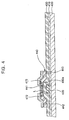
- the photoresist pattern 140 is removed, and a metal layer pattern or metal silicide layer pattern 145 is formed a predetermined distance apart from the channel region 136.
- the metal layer pattern or metal silicide layer pattern 145 is in contact with a region of the semiconductor layer 135 other than the channel region 136.
- depositing the metal layer pattern or metal silicide layer pattern 145 is followed by performing an annealing process to form a region 145a in the semiconductor layer 135, and a gettering process is performed using the region 145a.
- the crystallization-inducing metal is removed from the channel region 136 of the semiconductor layer 135 so that a leakage current may be reduced and the length L of the channel region 136 of the semiconductor layer 135 and the leakage current loff/W(A/mm) per 1 mm of the width W of the channel region 136 of the semiconductor layer 135 may satisfy Equation 1.
- the position of the metal layer pattern or metal silicide layer pattern 145 may be constant irrespective of the length L of the channel region 136.
- the length L of the channel region 136 may vary, and the metal layer pattern or metal silicide layer pattern 145 may be formed such that a distance between the channel region 136 and the metal layer pattern or metal silicide layer pattern 145 is constant with respect to the length L of the channel region 136.
- the metal layer pattern or metal silicide layer pattern 145 for gettering in the semiconductor layer 135 may be a metal layer pattern or metal silicide layer pattern including a metal or alloy thereof having a diffusion coefficient less than the crystallization-inducing metal 120a and 120b.
- the diffusion coefficient of the metal or metal silicide of the metal layer pattern or metal silicide layer pattern 145 in the semiconductor layer 135 may be 1% or less of the diffusion coefficient of the crystallization-inducing metal 120a and 120b. In this case, the metal or metal silicide of the metal layer pattern or metal silicide layer pattern 145 may be prevented from diffusing from the region 145a into the remaining region of the semiconductor layer 135.
- Ni may be used as the crystallization-inducing metal 120a and 120b used for the crystallization of the semiconductor layer 135.
- Ni has a diffusion coefficient of about 10 -5 cm 2 /s or less in the semiconductor layer 135. Therefore, when Ni is used as the crystallization-inducing metal 120a and 120b, the diffusion coefficient of the metal or metal silicide of the metal layer pattern or metal silicide layer pattern 145 used for gettering in the semiconductor layer 135 may be 1% or less of the diffusion coefficient of Ni.
- the metal or metal silicide may have a diffusion coefficient of 10 -7 cm 2 /s or less.
- the metal or metal silicide may be one selected from the group consisting of Sc, Ti, Zr, Hf, V, Nb, Ta, Cr, Mo, W, Mn, Re, Ru, Os, Co, Rh, Ir, Pt, Y, La, Ce, Pr, Nd, Dy, Ho, TiN, TaN, alloys thereof, and metal silicides thereof.
- the metal layer pattern or metal silicide layer pattern 145 may be formed to a thickness of about 3 to 1000 nm. When the metal layer pattern or metal silicide layer pattern 145 is formed to a thickness of less than about 3 nm, the crystallization-inducing metal may inefficiently getter into the region 145a of the semiconductor layer 135 that contacts the metal layer pattern or metal silicide layer pattern 145. When the metal layer pattern or metal silicide layer pattern 145 is formed to a thickness of more than about 1000 nm, the metal layer pattern or metal silicide layer pattern 145 may be delaminated due to thermal stress during a subsequent annealing process.
- a metal of the metal layer pattern may diffuse from the surface of the semiconductor layer 135 that contacts the metal layer pattern or metal silicide layer pattern 145 into the semiconductor layer 135 or combine with the semiconductor layer 135 to form a metal silicide.
- a metal silicide of the metal silicide layer pattern diffuses into the semiconductor layer 135.
- the region 145a containing a metal other than the crystallization-inducing metal or a metal silicide thereof is formed in a region of the semiconductor layer 135 that contacts the metal layer pattern or metal silicide layer pattern 145.
- the crystallization-inducing metal 120b When the crystallization-inducing metal remaining in the channel region 136 of the semiconductor layer 135 diffuses into the region 145a of the semiconductor layer 135 that contacts the metal layer pattern or metal silicide layer pattern 145 due to the annealing process, the crystallization-inducing metal 120b is precipitated in the region 145a and does not diffuse any more. This is because the crystallization-inducing metal 120b is thermodynamically more stable in the region 145a containing the other metal or a metal silicide thereof than in silicon. Based on this principle, the crystallization-inducing metal 120b may be removed from the channel region 136 of the semiconductor layer 135.
- the annealing process may be performed at a temperature of about 500 to 993°C for 10 seconds to 10 hours.
- the annealing process is performed at a temperature lower than 500°C, diffusion of the crystallization-inducing metal into the semiconductor layer 135 does not occur so that the crystallization-inducing metal 120b cannot move to the region 145a of the semiconductor layer 135.
- the annealing process is performed at a temperature higher than 993°C and Ni is used as the crystallization-inducing metal 120a and 120b, the Ni may be liquefied since Ni has a eutectic point of 993°C, and the substrate 100 may be deformed due to high heat.
- the annealing process when the annealing process is performed for a time shorter than 10 seconds, it may be difficult to sufficiently remove the crystallization-inducing metal 120b from the channel region 136 of the semiconductor layer 135.
- the long-duration annealing process gives rise to deformation of the substrate 100, increases the fabrication cost, and may decrease yield.
- the annealing process is performed at a sufficiently high temperature, it is possible to remove the crystallization-inducing metal 120b in a short time.
- the metal layer pattern or metal silicide layer pattern 145 is removed, and a gate insulating layer 150 is formed on the surface of the substrate 100 having the semiconductor layer 135.
- the gate insulating layer 150 may be a silicon oxide layer, a silicon nitride layer, or a multi-layer thereof.
- a metal layer (not shown) for a gate electrode is formed.
- the metal layer may be a single layer formed of AI or an Al alloy, such as Al-Nd, or a multiple layer formed by stacking an Al alloy on a Cr alloy or a Mo alloy. Photolithographic and etching processes are performed on the metal layer for the gate electrode, thereby forming a gate electrode 155 to correspond to the channel region 136 of the semiconductor layer 135.
- an interlayer insulating layer 160 is formed on the surface of the substrate 100 having the gate electrode 155.
- the interlayer insulating layer 160 may be a silicon nitride layer, a silicon oxide layer, or a multiple layer thereof.
- the interlayer insulating layer 160 and the gate insulating layer 150 are etched to form contact holes to expose the source and drain regions 137 and 138 of the semiconductor layer 135.
- Source and drain electrodes 167 and 168 are formed to be connected to the source and drain regions 137 and 138 through the contact holes.
- the source and drain electrodes 167 and 168 may be formed of one selected from the group consisting of molybdenum (Mo), chromium (Cr), tungsten (W), molybdenum tungsten (MoW), aluminum (Al), aluminum-neodymium (Al-Nd), titanium (Ti), titanium nitride (TiN), copper (Cu), a Mo alloy, an Al alloy, and a Cu alloy.
- the metal layer pattern or metal silicide layer pattern 145 and the gate electrode 155 or the source and drain electrodes 167 and 168 may be formed of the same material.
- the metal layer pattern or metal silicide layer pattern 145 may be simultaneously formed when the gate electrode 155 or the source and the drain electrodes 167 and 168 is formed.
- FIG. 4 is a cross-sectional view of a TFT according to another embodiment of the present invention.
- the TFT shown in FIG. 4 is generally the same as the TFT shown in FIGs. 1 and 2 except for the following description.
- a substrate 400 is prepared.
- a buffer layer 410 may be disposed on the substrate 400, as shown in this embodiment.
- a gate electrode 420 is disposed on the buffer layer 410.
- a gate insulating layer 430 is disposed on the gate electrode 420.
- a patterned semiconductor layer 440 is disposed on the gate insulating layer 430.
- the semiconductor layer 440 is a semiconductor layer crystallized by a method using a crystallization-inducing metal, such as an MIC technique, an MILC technique, or an SGS technique.
- the semiconductor layer 440 includes a channel region 441 and source and drain regions 442 and 443.
- the SGS technique is more appropriate than the MIC technique or the MILC technique in forming the semiconductor layer 440 because the SGS technique may maintain a low concentration of a crystallization-inducing metal diffusing into an a-Si layer.
- a length L( ⁇ m) of the channel region 441 of the semiconductor layer 440 and a leakage current loff(A) per 1 mm of a width W of the channel region 441 of the semiconductor layer 440 satisfy Equation 1:
- the leakage current may be controlled using the width W or length L of the channel region 441 of the semiconductor layer 440. Conversely, since the leakage current may be predicted, the length L or width W of the channel region 441 of the semiconductor layer 440 may be determined considering a leakage current to be controlled.
- a leakage current per 1 mm of the width W of the channel region 441 also decreases because of the more efficient removal of the crystallization-inducing metal from the channel region 441 using a region in which a metal other than the crystallization-inducing metal or metal silicide thereof is formed.
- a value loff/W can be 1.0x10 -12 A/mm or less due to a high gettering effect, so that the TFT can exhibit good characteristics in a display device.
- a region 460a in which either a metal other than the crystallization-inducing metal or a metal silicide thereof is formed is disposed to a predetermined depth from the surface of the semiconductor layer 135 in the semiconductor layer 440 and spaced apart from the channel region 441.
- the metal or the metal silicide is used for a gettering process.
- a gettering process is performed using the region 460a in which the metal or the metal silicide is formed, thereby removing the crystallization-inducing metal from the channel region 441 of the semiconductor layer 440.
- a leakage current may be reduced and the length L( ⁇ m) of the channel region 441 of the semiconductor layer 440 and the leakage current loff(A) per 1 mm of the width W of the channel region 441 of the semiconductor layer 440 may satisfy Equation 1.
- a distance between the channel region 441 and the region 460a in which either the metal other than the crystallization-inducing metal or the metal silicide thereof is formed may be constant irrespective of the length L of the channel region 441.
- Source and drain electrodes 472 and 473 are disposed on the semiconductor layer 440 and electrically connected to the source and drain regions 442 and 443, respectively, of the semiconductor layer 440. Thus, the TFT according to the present embodiment is completed.
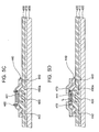
- FIGS. 5A through 5D are cross-sectional views of a process of fabricating the TFT shown in FIG. 4 .
- the process shown in FIGs. 5A through 5D is generally the same as the process shown in FIGs. 3A through 3G except for the following description.
- a buffer layer 410 is formed on a substrate 400.
- a metal layer (not shown) for a gate electrode is formed on the buffer layer 410 and etched using photolithographic and etching processes, thereby forming a gate electrode 420.
- a gate insulating layer 430 is formed on the substrate 400 having the gate electrode 420.
- an a-Si layer is formed on the gate insulating layer 430 and crystallized into a poly-Si layer using a crystallization-inducing metal as in the previous embodiment.
- the poly-Si layer is patterned to form a semiconductor layer 440.
- the poly-Si layer may be patterned during a subsequent process.
- a length and width of the semiconductor layer 135 are determined in consideration of Equation 1:
- a length L and a width W of a channel region of the semiconductor layer 440 are determined according to a leakage current to be controlled, and the length and width of the semiconductor layer 440 are determined in consideration of the length L and width W of the channel region.
- a leakage current per 1 mm of the width W of the channel region also decreases because of the more efficient removal of the crystallization-inducing metal from the channel region using a subsequent metal layer or metal silicide layer used for a gettering process.
- a value loff/W can be 1.0x10 -12 A/mmor less due to a high gettering effect, so that the resultant TFT can exhibit good characteristics in a display device.
- a photoresist pattern 450 is formed on a region of the semiconductor layer 440 where a channel region will be defined.
- Conductive impurity ions are doped into the semiconductor layer 440 using the photoresist pattern 450 as a mask, thereby forming a source region 442, a drain region 443, and a channel region 441 having a length L and a width W.
- the photoresist pattern 450 is removed, and a metal layer pattern or metal silicide layer pattern 460 is formed a predetermined distance apart from the channel region 441.
- the metal layer pattern or metal silicide layer pattern 460 is in contact with a region of the semiconductor layer 440 other than the channel region 441.
- depositing the metal layer pattern or metal silicide layer pattern 460 is followed by performing an annealing process to form a region 460a in the semiconductor layer 440, and a gettering process is performed using the region 460a.
- the crystallization-inducing metal is removed from the channel region 136 of the semiconductor layer 135 so that a leakage current may be reduced and the length L of the channel region 136 of the semiconductor layer 135 and the leakage current loff(A) per 1 mm of the width W of the channel region 136 of the semiconductor layer 135 may satisfy Equation 1.
- the position of the metal layer pattern or metal silicide layer pattern 460 may be constant irrespective of the length L of the channel region 441.
- the length L of the channel region 441 may vary, and the metal layer pattern or metal silicide layer pattern 460 may be formed such that a distance between the channel region 441 and the metal layer pattern or metal silicide layer pattern 460 is constant with respect to the length L of the channel region 441.
- an annealing process is performed in order to remove the crystallization-inducing metal from the semiconductor layer 440, especially, the channel region 441 of the semiconductor layer 440.
- a region 460a containing a metal other than the crystallization-inducing metal or a metal silicide thereof is formed in a region of the semiconductor layer 440 that contacts the metal layer pattern or metal silicide layer pattern 460.
- the region 460a is formed in the surface of the semiconductor layer 440 to a predetermined depth.
- the crystallization-inducing metal existing in the channel region 441 of the semiconductor layer 440 is gettered by diffusion into the region 460a.
- the annealing process is performed in a similar manner as described above.
- the metal layer pattern or metal silicide layer pattern 460 is removed, and a source/drain conductive layer is formed on the semiconductor layer 440 and patterned, thereby forming source and drain electrodes 472 and 473.
- a TFT including the gate electrode 420, the semiconductor layer 440, and the source and drain electrodes 472 and 473 is completed.
- FIG. 6 is a graph of leakage current loff(A) versus channel ratio (i.e., a channel width W(mm)/a channel length L( ⁇ m)) of a conventional TFT using a semiconductor layer crystallized using a crystallization-inducing metal.
- the abscissa denotes the channel ratio (i.e., the channel width W(mm)/the channel length L( ⁇ m))
- the ordinate denotes the leakage current loff(A).
- the leakage current loff(A) of the conventional TFT using the semiconductor layer crystallized using the crystallization-inducing metal shows no tendency but irregularly increases or decreases when the channel width W is 4, 10, and 50 mm, respectively, or when the channel length L ranges from 3 to 20 ⁇ m. Also, even if the channel ratio varies, the leakage current loff(A) varies within only a small range from 2.0x10 -12 to 4.0x10 -12 A, which makes no significant difference. Therefore, it can be seen that in the conventional TFT, the leakage current loff(A) is not effectively controlled by changing the channel ratio.
- FIG. 7 is a graph of leakage current loff(A) versus channel ratio of a TFT according to an embodiment of the present invention in which a metal layer pattern or metal silicide layer pattern for a gettering process is formed and annealed.
- the leakage current loff(A) was greatly reduced to approximately 5.0x10 -13 A. That is, when the metal layer pattern or metal silicide layer pattern for the gettering process is formed and annealed, it can be confirmed that a crystallization-inducing metal existing in a channel region is gettered.
- FIG. 8 is a graph of leakage current loff (A) per 1mm of the channel width W of a semiconductor layer versus channel length L ( ⁇ m) of a TFT according to an embodiment of the present invention.
- the abscissa denotes the channel length L( ⁇ m)
- the ordinate denotes the leakage current loff (A) per 1 mm of the channel width W.
- the leakage current loff shown in FIG. 7 is divided by the channel width W
- FIG. 8 shows leakage current loff/W divided by the channel width W versus channel length L.
- FIG. 9 is a graph of a function of a leakage current loff(A) per 1 mm of the channel width W of a semiconductor layer and the channel length L ( ⁇ m) of the TFT, which is obtained using regression analysis based on data shown in FIG. 8 .
- the abscissa denotes the channel length L ( ⁇ m)
- the ordinate denotes the leakage current loff(A) per 1 mm of the channel width W.
- the leakage current loff, the channel width W, and the channel length L are expressed in units of A, mm, and ⁇ m, respectively.
- the crystallization-inducing metal may be removed from the channel region of the semiconductor layer, thereby reducing the leakage current.
- the leakage current since the leakage current may be predicted according to the size of the channel region of the semiconductor layer, the leakage current may be determined by controlling the width W or length L of the channel region of the semiconductor layer. Conversely, the length L or width W of the channel region of the semiconductor layer may be determined considering the leakage current to be controlled.
- the width W of the channel region of the semiconductor layer is constant, as the length L of the channel region decreases, a leakage current per 1 mm of the width W of the channel region also decreases according to a secondary functional curve because of the more efficient removal of the crystallization-inducing metal from the channel region using the metal layer pattern or metal silicide layer pattern for a gettering process.
- the length L of the channel region is more than 0 and 15 ⁇ m or less, the value loff/W can be 1.0x10 -12 A or less due to a high gettering effect, so that the resultant TFT can exhibit good characteristics as a display device.
- FIG. 10 is a cross-sectional view of an organic light emitting diode (OLED) display device including the TFT shown in FIG. 1 .
- OLED organic light emitting diode
- FIG. 10 an insulating layer 170 is formed on the surface of the substrate 100 having the TFT shown in FIG. 3G , according to the present embodiment.
- the insulating layer 170 may be an inorganic layer selected from the group consisting of a silicon oxide layer, a silicon nitride layer, and a silicon on glass (SOG) layer, an organic layer formed of one selected from the group consisting of polyimide, benzocyclobutene (BCB) series resin, and acrylate, or a stacked layer of the inorganic layer and the organic layer.
- a silicon oxide layer selected from the group consisting of a silicon oxide layer, a silicon nitride layer, and a silicon on glass (SOG) layer
- an organic layer formed of one selected from the group consisting of polyimide, benzocyclobutene (BCB) series resin, and acrylate or a stacked layer of the inorganic layer and the organic layer.
- the insulating layer 170 may be etched to form a via hole exposing one of the source and drain electrodes 167 and 168.
- a first electrode 175 is formed and connected to one of the source and drain electrodes 167 and 168 through the via hole.
- the first electrode 175 may be an anode or a cathode.
- the anode may be formed of a transparent conductive material selected from the group consisting of indium tin oxide (ITO), indium zinc oxide (IZO), and indium tin zinc oxide (ITZO).
- ITO indium tin oxide
- IZO indium zinc oxide
- ITZO indium tin zinc oxide
- the cathode may be formed of one selected from the group consisting of Mg, Ca, Al, Ag, Ba, and alloys thereof.
- a pixel defining layer 180 is formed on the first electrode 175 to have an opening that exposes a portion of the first electrode 175.
- An organic layer 185 including an emission layer (EML) is formed on the exposed portion of the first electrode 175.
- the organic layer 185 may further include a hole injection layer (HIL), a hole transport layer (HTL), a hole blocking layer (HBL), an electron blocking layer (EBL), an electron injection layer (EIL), and an electron transport layer (ETL), among other layers.
- HIL hole injection layer
- HTL hole transport layer
- HBL hole blocking layer
- EBL electron blocking layer
- EIL electron injection layer
- ETL electron transport layer
- a region in which either a metal other than a crystallization-inducing metal or a metal silicide thereof is formed is disposed in a semiconductor layer crystallized using the crystallization-inducing metal.
- the region in which the metal or metal silicide is formed is spaced apart from a channel region of the semiconductor layer and extends from the surface of the semiconductor layer to a predetermined depth.
- a gettering process is performed using the region in which the metal or the metal silicide is formed, thereby removing the crystallization-inducing metal from the channel region of the semiconductor layer. As a result, a leakage current may be decreased.
- the leakage current may be predicted according to the size of the channel region of the semiconductor layer, the leakage current may be determined by controlling the width W or length L of the channel region of the semiconductor layer. Conversely, the width W or length L of the channel region of the semiconductor layer may be determined considering a leakage current to be controlled.
- the crystallization-inducing metal in a TFT including a semiconductor layer crystallized using a crystallization-inducing metal, can be removed from a channel region of the semiconductor layer. As a result, a leakage current can be reduced. Also, the leakage current can be predicted according to the width or length of the channel region of the semiconductor layer. Furthermore, the width or length of the channel region of the semiconductor layer may be determined considering a leakage current to be controlled.
- aspects of the present invention are described in association with an organic light emitting diode display devices, the aspects of the present invention are not limited thereto such that the thin film transistor according to the aspects of the present invention may be used with other display devices, such as liquid crystal displays and plasma display paneis.
Landscapes
- Thin Film Transistor (AREA)
- Recrystallisation Techniques (AREA)
- Electroluminescent Light Sources (AREA)
- Electrodes Of Semiconductors (AREA)
Applications Claiming Priority (1)
| Application Number | Priority Date | Filing Date | Title |
|---|---|---|---|
| KR1020070057900A KR100848341B1 (ko) | 2007-06-13 | 2007-06-13 | 박막트랜지스터, 그의 제조방법, 및 이를 포함하는유기전계발광표시장치 |
Publications (2)
| Publication Number | Publication Date |
|---|---|
| EP2003695A2 true EP2003695A2 (de) | 2008-12-17 |
| EP2003695A3 EP2003695A3 (de) | 2011-08-10 |
Family
ID=39791336
Family Applications (1)
| Application Number | Title | Priority Date | Filing Date |
|---|---|---|---|
| EP08252041A Withdrawn EP2003695A3 (de) | 2007-06-13 | 2008-06-13 | Dünnfilmtransistor, Verfahren zur Herstellung des Dünnfilmtransistors und Anzeigegerät mit dem Dünnfilmtransistor |
Country Status (6)
| Country | Link |
|---|---|
| US (1) | US7838885B2 (de) |
| EP (1) | EP2003695A3 (de) |
| JP (1) | JP5091017B2 (de) |
| KR (1) | KR100848341B1 (de) |
| CN (1) | CN101325220B (de) |
| TW (1) | TWI377681B (de) |
Cited By (6)
| Publication number | Priority date | Publication date | Assignee | Title |
|---|---|---|---|---|
| EP2146371A1 (de) * | 2008-07-14 | 2010-01-20 | Samsung Mobile Display Co., Ltd. | Dünnschichttransistor, Herstellungsverfahren dafür und organische LED-Anzeigevorrichtung mit dem Dünnschichttransistor |
| US8101952B2 (en) | 2008-03-27 | 2012-01-24 | Samsung Mobile Display Co., Ltd. | Thin film transistor, method of fabricating the same, and organic lighting emitting diode display device including the same |
| US8283668B2 (en) | 2007-08-23 | 2012-10-09 | Samsung Display Co., Ltd. | Thin film transistor, method of fabricating the same, and organic light emitting diode display device including the same |
| US8318523B2 (en) | 2008-04-11 | 2012-11-27 | Samsung Display Co., Ltd. | Thin film transistor, method of fabricating the same and organic light emitting diode display device having the same |
| US8513669B2 (en) | 2007-08-22 | 2013-08-20 | Samsung Display Co., Ltd. | Thin film transistor including metal or metal silicide structure in contact with semiconductor layer and organic light emitting diode display device having the thin film transistor |
| US8790967B2 (en) | 2007-05-31 | 2014-07-29 | Samsung Display Co., Ltd. | Method of fabricating polycrystalline silicon layer, TFT fabricated using the same, method of fabricating TFT, and organic light emitting diode display device having the same |
Families Citing this family (13)
| Publication number | Priority date | Publication date | Assignee | Title |
|---|---|---|---|---|
| KR101043953B1 (ko) | 2009-05-29 | 2011-06-24 | 전자부품연구원 | 박막 트랜지스터 제조방법 및 제조된 박막 트랜지스터 |
| CN104681568B (zh) | 2009-10-21 | 2017-11-21 | 株式会社半导体能源研究所 | 显示装置和包括显示装置的电子设备 |
| WO2011058865A1 (en) * | 2009-11-13 | 2011-05-19 | Semiconductor Energy Laboratory Co., Ltd. | Semiconductor devi ce |
| TWI555205B (zh) * | 2010-11-05 | 2016-10-21 | 半導體能源研究所股份有限公司 | 半導體裝置及半導體裝置的製造方法 |
| CN102810569A (zh) * | 2011-06-01 | 2012-12-05 | 广东中显科技有限公司 | 可同时驱入镍和调整阈值电压的多晶硅薄膜晶体管 |
| KR101809661B1 (ko) * | 2011-06-03 | 2017-12-18 | 삼성디스플레이 주식회사 | 박막 트랜지스터, 그 제조 방법 및 이를 포함하는 유기 발광 표시 장치 |
| KR102239841B1 (ko) * | 2014-08-06 | 2021-04-14 | 삼성디스플레이 주식회사 | 박막 트랜지스터, 이를 구비하는 디스플레이 장치, 박막 트랜지스터의 제조방법 및 디스플레이 장치의 제조방법 |
| CN104143533B (zh) * | 2014-08-07 | 2017-06-27 | 深圳市华星光电技术有限公司 | 高解析度amoled背板制造方法 |
| CN107533979B (zh) * | 2015-04-20 | 2020-11-10 | 堺显示器制品株式会社 | 薄膜晶体管的制造方法和显示面板 |
| CN106298547A (zh) * | 2016-08-12 | 2017-01-04 | 烟台南山学院 | 一种新型非晶氧化物薄膜晶体管的高效退火方法 |
| CN106356378B (zh) | 2016-09-26 | 2023-10-27 | 合肥鑫晟光电科技有限公司 | 阵列基板及其制作方法 |
| CN110391264A (zh) * | 2018-04-19 | 2019-10-29 | 群创光电股份有限公司 | 电子装置 |
| US11521972B2 (en) * | 2020-05-01 | 2022-12-06 | Tokyo Electron Limited | High performance multi-dimensional device and logic integration |
Family Cites Families (26)
| Publication number | Priority date | Publication date | Assignee | Title |
|---|---|---|---|---|
| JP3844552B2 (ja) * | 1997-02-26 | 2006-11-15 | 株式会社半導体エネルギー研究所 | 半導体装置の作製方法 |
| JP3974229B2 (ja) * | 1997-07-22 | 2007-09-12 | 株式会社半導体エネルギー研究所 | 半導体装置の作製方法 |
| JPH11261075A (ja) * | 1998-03-13 | 1999-09-24 | Semiconductor Energy Lab Co Ltd | 半導体装置およびその作製方法 |
| US6346437B1 (en) | 1998-07-16 | 2002-02-12 | Sharp Laboratories Of America, Inc. | Single crystal TFT from continuous transition metal delivery method |
| US6294441B1 (en) * | 1998-08-18 | 2001-09-25 | Semiconductor Energy Laboratory Co., Ltd. | Method of manufacturing a semiconductor device |
| TW473800B (en) | 1999-12-28 | 2002-01-21 | Semiconductor Energy Lab | Method of manufacturing a semiconductor device |
| JP2001319878A (ja) * | 2000-05-11 | 2001-11-16 | Sharp Corp | 半導体製造方法 |
| KR100439345B1 (ko) * | 2000-10-31 | 2004-07-07 | 피티플러스(주) | 폴리실리콘 활성층을 포함하는 박막트랜지스터 및 제조 방법 |
| US7045444B2 (en) | 2000-12-19 | 2006-05-16 | Semiconductor Energy Laboratory Co., Ltd. | Method of manufacturing semiconductor device that includes selectively adding a noble gas element |
| JP4712197B2 (ja) * | 2001-01-29 | 2011-06-29 | 株式会社半導体エネルギー研究所 | 半導体装置の作製方法 |
| JP3961240B2 (ja) * | 2001-06-28 | 2007-08-22 | 株式会社半導体エネルギー研究所 | 半導体装置の作製方法 |
| JP2003100633A (ja) | 2001-09-25 | 2003-04-04 | Sharp Corp | 半導体装置の製造方法および半導体装置 |
| JP2003188098A (ja) | 2001-12-13 | 2003-07-04 | Sharp Corp | 半導体装置およびその製造方法 |
| JP3961310B2 (ja) * | 2002-02-21 | 2007-08-22 | 株式会社半導体エネルギー研究所 | 半導体装置の作製方法 |
| KR100488959B1 (ko) | 2002-03-08 | 2005-05-11 | 비오이 하이디스 테크놀로지 주식회사 | 다결정 실리콘 박막트랜지스터의 제조 방법 |
| JP2003318403A (ja) * | 2002-04-23 | 2003-11-07 | Sharp Corp | 半導体装置およびその製造方法 |
| JP4115252B2 (ja) * | 2002-11-08 | 2008-07-09 | シャープ株式会社 | 半導体膜およびその製造方法ならびに半導体装置およびその製造方法 |
| JP4115283B2 (ja) * | 2003-01-07 | 2008-07-09 | シャープ株式会社 | 半導体装置およびその製造方法 |
| KR100666564B1 (ko) * | 2004-08-04 | 2007-01-09 | 삼성에스디아이 주식회사 | 박막트랜지스터의 제조 방법 |
| KR100611766B1 (ko) * | 2004-08-24 | 2006-08-10 | 삼성에스디아이 주식회사 | 박막트랜지스터 제조 방법 |
| KR200369852Y1 (ko) | 2004-09-24 | 2004-12-09 | 성원이엔티 주식회사 | 폐 콘크리트 재생 골재 제조장치의 세척수 중화장치 |
| KR200373076Y1 (ko) | 2004-10-12 | 2005-01-15 | 황금수 | 톱밥제조기용 칼날고정장치 및 그 칼날 |
| KR20060099694A (ko) | 2005-03-14 | 2006-09-20 | 삼성전자주식회사 | 게터링사이트층을 구비하는 반도체 기판 및 그 형성 방법 |
| TWI545380B (zh) * | 2006-05-16 | 2016-08-11 | 半導體能源研究所股份有限公司 | 液晶顯示裝置和半導體裝置 |
| KR100875432B1 (ko) * | 2007-05-31 | 2008-12-22 | 삼성모바일디스플레이주식회사 | 다결정 실리콘층의 제조 방법, 이를 이용하여 형성된박막트랜지스터, 그의 제조방법 및 이를 포함하는유기전계발광표시장치 |
| KR200441074Y1 (ko) | 2008-03-27 | 2008-07-21 | 조동명 | 철도차량 보수용 리프트 대차 |
-
2007
- 2007-06-13 KR KR1020070057900A patent/KR100848341B1/ko not_active Expired - Fee Related
-
2008
- 2008-06-10 JP JP2008152204A patent/JP5091017B2/ja active Active
- 2008-06-11 TW TW097121812A patent/TWI377681B/zh active
- 2008-06-13 CN CN200810125129.XA patent/CN101325220B/zh active Active
- 2008-06-13 EP EP08252041A patent/EP2003695A3/de not_active Withdrawn
- 2008-06-13 US US12/138,884 patent/US7838885B2/en active Active
Cited By (9)
| Publication number | Priority date | Publication date | Assignee | Title |
|---|---|---|---|---|
| US8790967B2 (en) | 2007-05-31 | 2014-07-29 | Samsung Display Co., Ltd. | Method of fabricating polycrystalline silicon layer, TFT fabricated using the same, method of fabricating TFT, and organic light emitting diode display device having the same |
| EP2009680B1 (de) * | 2007-05-31 | 2015-04-01 | Samsung Display Co., Ltd. | Verfahren zur Herstellung einer Polykristallinsiliziumschicht |
| US8513669B2 (en) | 2007-08-22 | 2013-08-20 | Samsung Display Co., Ltd. | Thin film transistor including metal or metal silicide structure in contact with semiconductor layer and organic light emitting diode display device having the thin film transistor |
| US8283668B2 (en) | 2007-08-23 | 2012-10-09 | Samsung Display Co., Ltd. | Thin film transistor, method of fabricating the same, and organic light emitting diode display device including the same |
| US8101952B2 (en) | 2008-03-27 | 2012-01-24 | Samsung Mobile Display Co., Ltd. | Thin film transistor, method of fabricating the same, and organic lighting emitting diode display device including the same |
| US8436360B2 (en) | 2008-03-27 | 2013-05-07 | Samsung Display Co., Ltd. | Thin film transistor, method of fabricating the same, and organic lighting emitting diode display device including the same |
| US8318523B2 (en) | 2008-04-11 | 2012-11-27 | Samsung Display Co., Ltd. | Thin film transistor, method of fabricating the same and organic light emitting diode display device having the same |
| EP2146371A1 (de) * | 2008-07-14 | 2010-01-20 | Samsung Mobile Display Co., Ltd. | Dünnschichttransistor, Herstellungsverfahren dafür und organische LED-Anzeigevorrichtung mit dem Dünnschichttransistor |
| US8253141B2 (en) | 2008-07-14 | 2012-08-28 | Samsung Mobile Display Co., Ltd. | Thin film transistor, method of fabricating the same, and organic light emitting diode display device including the thin film transistor |
Also Published As
| Publication number | Publication date |
|---|---|
| KR100848341B1 (ko) | 2008-07-25 |
| TW200908337A (en) | 2009-02-16 |
| US20080308809A1 (en) | 2008-12-18 |
| EP2003695A3 (de) | 2011-08-10 |
| CN101325220A (zh) | 2008-12-17 |
| US7838885B2 (en) | 2010-11-23 |
| TWI377681B (en) | 2012-11-21 |
| JP5091017B2 (ja) | 2012-12-05 |
| JP2008311649A (ja) | 2008-12-25 |
| CN101325220B (zh) | 2011-03-23 |
Similar Documents
| Publication | Publication Date | Title |
|---|---|---|
| US7838885B2 (en) | Thin film transistor, method of fabricating the thin film transistor, and display device including the thin film transistor | |
| US8513669B2 (en) | Thin film transistor including metal or metal silicide structure in contact with semiconductor layer and organic light emitting diode display device having the thin film transistor | |
| US8445336B2 (en) | Method of fabricating polycrystalline silicon, TFT fabricated using the same, method of fabricating the TFT, and organic light emitting diode display device including the TFT | |
| EP2009680B1 (de) | Verfahren zur Herstellung einer Polykristallinsiliziumschicht | |
| US8283668B2 (en) | Thin film transistor, method of fabricating the same, and organic light emitting diode display device including the same | |
| EP2083440B1 (de) | Verfahren zur Herstellung eines Dünnfilmtransistors | |
| US8409887B2 (en) | Organic light emitting diode display device and method of fabricating the same | |
| EP2226833B1 (de) | Herstellungsverfahren eines Dünnschichttransistors | |
| EP1939933A2 (de) | Dünnschichttransistor, Herstellungsverfahren dafür und organische lichtemittierende Diodenanzeigevorrichtung damit | |
| EP2146371B1 (de) | Herstellungsverfahren für Dünnschichttransistor | |
| EP2117048B1 (de) | Dünnschichttransistor, Herstellungsverfahren dafür und organische LED-Anzeigevorrichtung damit | |
| US8288216B2 (en) | Thin film transistor and method of fabricating the same | |
| EP2226848A1 (de) | Dünnschichttransistor, Herstellungsverfahren dafür und organische LED-Anzeigevorrichtung damit |
Legal Events
| Date | Code | Title | Description |
|---|---|---|---|
| PUAI | Public reference made under article 153(3) epc to a published international application that has entered the european phase |
Free format text: ORIGINAL CODE: 0009012 |
|
| 17P | Request for examination filed |
Effective date: 20080626 |
|
| AK | Designated contracting states |
Kind code of ref document: A2 Designated state(s): AT BE BG CH CY CZ DE DK EE ES FI FR GB GR HR HU IE IS IT LI LT LU LV MC MT NL NO PL PT RO SE SI SK TR |
|
| AX | Request for extension of the european patent |
Extension state: AL BA MK RS |
|
| RIN1 | Information on inventor provided before grant (corrected) |
Inventor name: PARK, BYOUNG-KEON Inventor name: SEO, JIN-WOOK Inventor name: YANG, TAE-HOON Inventor name: LEE, KI-YONGC |
|
| RAP1 | Party data changed (applicant data changed or rights of an application transferred) |
Owner name: SAMSUNG MOBILE DISPLAY CO., LTD. |
|
| PUAL | Search report despatched |
Free format text: ORIGINAL CODE: 0009013 |
|
| AK | Designated contracting states |
Kind code of ref document: A3 Designated state(s): AT BE BG CH CY CZ DE DK EE ES FI FR GB GR HR HU IE IS IT LI LT LU LV MC MT NL NO PL PT RO SE SI SK TR |
|
| AX | Request for extension of the european patent |
Extension state: AL BA MK RS |
|
| RIC1 | Information provided on ipc code assigned before grant |
Ipc: H01L 21/77 20060101ALI20110707BHEP Ipc: H01L 27/12 20060101AFI20110707BHEP |
|
| AKX | Designation fees paid |
Designated state(s): DE FR GB |
|
| STAA | Information on the status of an ep patent application or granted ep patent |
Free format text: STATUS: THE APPLICATION IS DEEMED TO BE WITHDRAWN |
|
| 18D | Application deemed to be withdrawn |
Effective date: 20140103 |