EP2003783A9 - Digitales verarbeitungsgerät - Google Patents
Digitales verarbeitungsgerät Download PDFInfo
- Publication number
- EP2003783A9 EP2003783A9 EP07741163A EP07741163A EP2003783A9 EP 2003783 A9 EP2003783 A9 EP 2003783A9 EP 07741163 A EP07741163 A EP 07741163A EP 07741163 A EP07741163 A EP 07741163A EP 2003783 A9 EP2003783 A9 EP 2003783A9
- Authority
- EP
- European Patent Office
- Prior art keywords
- frequency
- rotating vector
- digital
- converter
- output
- Prior art date
- Legal status (The legal status is an assumption and is not a legal conclusion. Google has not performed a legal analysis and makes no representation as to the accuracy of the status listed.)
- Withdrawn
Links
Images


Classifications
-
- H—ELECTRICITY
- H03—ELECTRONIC CIRCUITRY
- H03M—CODING; DECODING; CODE CONVERSION IN GENERAL
- H03M1/00—Analogue/digital conversion; Digital/analogue conversion
- H03M1/06—Continuously compensating for, or preventing, undesired influence of physical parameters
- H03M1/0617—Continuously compensating for, or preventing, undesired influence of physical parameters characterised by the use of methods or means not specific to a particular type of detrimental influence
- H03M1/0634—Continuously compensating for, or preventing, undesired influence of physical parameters characterised by the use of methods or means not specific to a particular type of detrimental influence by averaging out the errors, e.g. using sliding scale
- H03M1/0636—Continuously compensating for, or preventing, undesired influence of physical parameters characterised by the use of methods or means not specific to a particular type of detrimental influence by averaging out the errors, e.g. using sliding scale in the amplitude domain
- H03M1/0639—Continuously compensating for, or preventing, undesired influence of physical parameters characterised by the use of methods or means not specific to a particular type of detrimental influence by averaging out the errors, e.g. using sliding scale in the amplitude domain using dither, e.g. using triangular or sawtooth waveforms
- H03M1/0641—Continuously compensating for, or preventing, undesired influence of physical parameters characterised by the use of methods or means not specific to a particular type of detrimental influence by averaging out the errors, e.g. using sliding scale in the amplitude domain using dither, e.g. using triangular or sawtooth waveforms the dither being a random signal
-
- H—ELECTRICITY
- H03—ELECTRONIC CIRCUITRY
- H03L—AUTOMATIC CONTROL, STARTING, SYNCHRONISATION OR STABILISATION OF GENERATORS OF ELECTRONIC OSCILLATIONS OR PULSES
- H03L7/00—Automatic control of frequency or phase; Synchronisation
- H03L7/06—Automatic control of frequency or phase; Synchronisation using a reference signal applied to a frequency- or phase-locked loop
- H03L7/08—Details of the phase-locked loop
- H03L7/085—Details of the phase-locked loop concerning mainly the frequency- or phase-detection arrangement including the filtering or amplification of its output signal
- H03L7/091—Details of the phase-locked loop concerning mainly the frequency- or phase-detection arrangement including the filtering or amplification of its output signal the phase or frequency detector using a sampling device
-
- H—ELECTRICITY
- H03—ELECTRONIC CIRCUITRY
- H03L—AUTOMATIC CONTROL, STARTING, SYNCHRONISATION OR STABILISATION OF GENERATORS OF ELECTRONIC OSCILLATIONS OR PULSES
- H03L7/00—Automatic control of frequency or phase; Synchronisation
- H03L7/06—Automatic control of frequency or phase; Synchronisation using a reference signal applied to a frequency- or phase-locked loop
- H03L7/08—Details of the phase-locked loop
- H03L7/10—Details of the phase-locked loop for assuring initial synchronisation or for broadening the capture range
- H03L7/104—Details of the phase-locked loop for assuring initial synchronisation or for broadening the capture range using an additional signal from outside the loop for setting or controlling a parameter in the loop
-
- H—ELECTRICITY
- H03—ELECTRONIC CIRCUITRY
- H03L—AUTOMATIC CONTROL, STARTING, SYNCHRONISATION OR STABILISATION OF GENERATORS OF ELECTRONIC OSCILLATIONS OR PULSES
- H03L7/00—Automatic control of frequency or phase; Synchronisation
- H03L7/06—Automatic control of frequency or phase; Synchronisation using a reference signal applied to a frequency- or phase-locked loop
- H03L7/08—Details of the phase-locked loop
- H03L7/10—Details of the phase-locked loop for assuring initial synchronisation or for broadening the capture range
- H03L7/113—Details of the phase-locked loop for assuring initial synchronisation or for broadening the capture range using frequency discriminator
-
- H—ELECTRICITY
- H03—ELECTRONIC CIRCUITRY
- H03L—AUTOMATIC CONTROL, STARTING, SYNCHRONISATION OR STABILISATION OF GENERATORS OF ELECTRONIC OSCILLATIONS OR PULSES
- H03L7/00—Automatic control of frequency or phase; Synchronisation
- H03L7/06—Automatic control of frequency or phase; Synchronisation using a reference signal applied to a frequency- or phase-locked loop
- H03L7/16—Indirect frequency synthesis, i.e. generating a desired one of a number of predetermined frequencies using a frequency- or phase-locked loop
- H03L7/18—Indirect frequency synthesis, i.e. generating a desired one of a number of predetermined frequencies using a frequency- or phase-locked loop using a frequency divider or counter in the loop
- H03L7/183—Indirect frequency synthesis, i.e. generating a desired one of a number of predetermined frequencies using a frequency- or phase-locked loop using a frequency divider or counter in the loop a time difference being used for locking the loop, the counter counting between fixed numbers or the frequency divider dividing by a fixed number
-
- H—ELECTRICITY
- H03—ELECTRONIC CIRCUITRY
- H03M—CODING; DECODING; CODE CONVERSION IN GENERAL
- H03M1/00—Analogue/digital conversion; Digital/analogue conversion
- H03M1/12—Analogue/digital converters
Definitions
- the present invention relates to a spurious reduction system of a digital processor obtaining analog signals through an analog/digital (A/D) converter, and is concerned with prevention of a mal function of the A/D converter especially in a PLL system frequency synthesizer
- the digital processor of this sort includes, for instance, a radio communication device such as a cellular phone, a waveform analyzer, a frequency synthesizer and the like.
- the frequency synthesizer includes a device to which a phase locked loop (PLL) shown in FIG. 18 is applied, and further includes a phase comparison function configured with a programmable logic device (PLD).
- PLL phase locked loop
- PLD programmable logic device
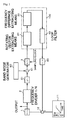
- the PLL works such that it divides an oscillation output of a voltage controlled oscillator 101 into 1/N with a divider 102, inputs the divided output into one input terminal of a phase comparator 103, and at the same time, divides an oscillation output 104 of, for instance, a crystal oscillator 104 being a reference signal generator into 1/M with a divider 100, inputs the divided output into the other input terminal of the phase comparator 103, and feeds back the compared signal to the voltage controlled oscillator 101 via a loop filter 105.
- the frequency synthesizer is able to switch an output frequency of the voltage controlled oscillator 101 in a wide frequency range in steps of 1 MHz or the like by changing the frequency divider ratios of the dividers 100 and 102 with an outside circuit, and further, by forming the PLL in a multiple configuration.
- the oscillation output of the voltage controlled oscillator 101 is converted into a digital signal at the A/D converter, the digital signal and the oscillation output (clock signal) of the quartz oscillator 104 are captured into a digital processing circuit to perform a phase comparison processing, and the comparison result is restored to an analog signal at a D/A converter to be a voltage controlled signal of the voltage controlled oscillator 101.
- Patent Document 1 there is a description that M-series pseudo-random numbers uncorrelated to each other are generated, and digitally added. Then, they are subjected to D/A conversion, and analogously added to an analog input signal to be an input of the A/D converter.
- a band noise generator since a band noise generator is not used, a considerably large output level is generated even within an output frequency of the A/D converter.
- the circuit is used in the device, and if it is used for restraint of spurious generation with the advance of charge/discharge of the holding current of the A/D converter, it affects the signal processing at the subsequent stage.
- An object of the present invention is to provide a digital processor that reduces spurious generation due to a malfunction of an A/D converter in a device conducting digital processing by converting an analog signal of high cyclic characteristics into a digital signal at an A/D converter
- a digital processor of the present invention includes an analog/digital converter into which an analog input signal of high cyclic characteristics is input; a band noise generator generating noise in a prescribed frequency band; an adder for adding noise generated in the band noise generator to the input signal of the above-described analog/digital converter; and a digital processing unit executing digital processing based on a digital signal converted by the above-described analog/digital converter, in which the frequency band of the noise outputted from the above-described noise generator is a band not affecting the digital signal processing in the above-described digital processing unit.
- the following example can be cited for instance.
- a configuration further including: a voltage controlled oscillator provided on an input side of the above-described analog/digital converter; and a digital/analog converter provided on an output side of the above-described digital processing unit, in which a PLL loop is formed by feeding back a signal processed by the above-described digital processing unit to the voltage controlled oscillator via the above-described digital/analog converter.
- a frequency synthesizer can be cited for example.
- noise from the band noise generator is added to the input side of the A/D converter, and since the frequency band of the above-described noise is a band not affecting digital signal processing in the above-described digital processing unit, it is possible to reduce spurious generation due to a malfunction of an A/D converter to which an analog signal of high cyclic characteristics is inputted.
- FIG. 1 is a view showing an embodiment in which a digital processor of the present invention is applied to a frequency synthesizer.
- the frequency synthesizer operates based on a new principle
- the present invention is not limited to be applied to this kind of frequency synthesizer, but can be widely applied to a device to A/D-convert an input signal of high cyclic characteristics and to perform digital processing of the output. Accordingly, an outline of the new frequency synthesizer will be explained only simply at the time before an explanation of the present invention, and a detailed configuration of the frequency synthesizer will be described after completion of the explanation of the present invention.
- FIG. 1 an operation principle of the frequency synthesizer will be briefly explained referring to FIG. 1 . In FIG.
- 1, "1" is a voltage controlled oscillator as a voltage controlled oscillation unit, which outputs a frequency signal which is a rectangular wave having a frequency corresponding to a supplied voltage.
- the frequency signal from the voltage controlled oscillator 1 is divided in 1/N (N is an integer) by a frequency dividing means 2, and converted into a sine wave further to be converted into a digital signal.
- the conversion corresponds to processing to extract a rotating vector rotating at a frequency (speed) corresponding to a frequency of the above-described frequency signal by a rotating vector extracting means 20.
- a frequency difference extracting means 30 at the subsequent stage of the rotating vector extracting means 20 extracts the difference between a frequency of the above-described rotating vector and a frequency fr of the rotating vector when an output frequency of the voltage controlled oscillator 1 becomes a set frequency.
- a method of extracting the frequency difference for instance, a method can be cited, in which an inverse rotating vector rotating at a frequency fr in the opposite direction to the rotational direction of a rotating vector extracted by the rotating vector extracting means 20 when the output frequency of the voltage controlled oscillator 1 becomes a set frequency is prepared, the above-described rotating vector and the inverse rotating vector are multiplied and a frequency difference therebetween is extracted.
- the frequency of the rotating vector is reduced in some extent with an inverse rotating vector and a remaining frequency difference portion, for instance, the speed of a rotating vector may be detected with an approximate expression.
- adjustment to make the frequency of a rotating vector coincide with fr is divided into rough adjustment and fine adjustment.
- n is an integer
- n is an integer
- an inverse rotating vector inversely rotating at the frequency n•fa is multiplied by the above-described rotating vector, and a very slowly rotating vector of frequency obtained by deducting the frequency of the inverse rotating vector from the frequency of the above-described rotating vector is extracted.
- a frequency m•fb (m is an integer) which is closest to the difference between fr and the above-described frequency n•fa is calculated, the difference between the frequency of the above-described very slowly rotating vector and the frequency m•fb is extracted, and thus, the difference between the frequency of a rotating vector obtained by the rotating vector extracting means and fr is determined.
- the voltage corresponding to a frequency difference extracted by the frequency difference extracting means 30 is negatively fed back from a loop filter 40 being an integrating means to the input side of the voltage controlled oscillator 1, and an input voltage of the voltage controlled oscillator 1 is deducted from a voltage output unit 11 for frequency pull-in by this amount of voltage.
- the voltage for the frequency pull-in is supplied to the voltage controlled oscillator 1, and when the loop operates, a voltage corresponding to the above-described frequency difference is integrated in the loop filter 40, a voltage corresponding to the integrated value is added to be inputted into the voltage controlled oscillator 1, and the above-described frequency difference becomes small as the output frequency comes close to the set frequency.
- the manner of the increase in the integrated value becomes small, and when the above-described frequency. difference comes to zero, the PLL is locked, so that the output frequency of the voltage controlled oscillator 1 is locked to the set frequency.
- the input voltage is linearly increased, for instance, in relation to time, the output frequency is increased as the increase of the input voltage, and the frequency of the rotating vector extracted by the rotating vector extracting means 20 is increased.
- this frequency comes in a controllable range of the PLL, the difference between the frequency fr of the rotating vector at the time when the output frequency of the voltage controlled oscillator 1 comes to the set frequency and the frequency of the rotating vector, becomes small.
- an amount of the feed back becomes small.
- An oscillation output of the voltage controlled oscillator is input into a lowpass filter 21 via a frequency divider 2 to be extracted as a sinusoidal wave signal having only a fundamental wave component, and the sinusoidal wave signal is input into an A/D converter 3.
- a sampling clock of 40 MHz is input from a digital processing unit 100.
- the rotating vector extracting means 20, the frequency difference extracting means 30 and the loop filter 40 compose the digital processing unit 100, and the digital processing unit 100 is configured with a digital processor device, for instance, a field programmable gate array (FPGA).
- a band noise generator 90 is provided, and an output of the band noise generator 90 is added to an analog output of the lowpass filter 21 with an adder 91 to designate this as a conversion input of the A/D converter 3.
- a band noise generator 90 it is possible to cite a configuration that, for instance, a pseudo-random pulse is generated from digital processing to convert this to an analog signal, so that a band noise output close to a white noise is obtained. It is necessary for the frequency band of this noise to be a band not affecting digital signal processing in the above-described digital processing unit. Accordingly, it is necessary for the signal level of the above-described noise to be sufficiently small compared with the level of the input signal of the A/D converter 3 in the output frequency of the A/D converter 3. For its frequency characteristics, as shown in FIG.
- the filter 2 for instance, it may have a frequency band at a position lower than the output frequency of the A/D converter 3, or conversely, it may have a frequency band at a position higher than the above-described output frequency.
- a filter to eliminate low frequencies is generally provided on the subsequent stage side of the A/D converter 3, namely, in the FPGA being the digital processing unit 100, it is one of preferable embodiments to set the noise frequency band in a band removed by the filter.
- FIG. 3 shows an example of a band noise output waveform by the band noise generator 90, and it is possible to obtain a band noise whose noise center frequency is 20 MHz. Note that the portion with slant lines corresponds to a part to record a signal waveform, and its waveform image is expressed in black because the gap between pulses is narrower than the resolving power of the image.
- noise is generated by the band noise generator 90, and it is possible to reduce spurious generation due to a malfunction of the A/D converter 3 by adding the noise to an analog input of the A/D converter 3.
- this will be explained concretely.
- FIG. 4 shows the timing of sampling of an input signal of the A/D converter 3 and an outline of the inside circuit of the A/D converter 3.
- a switche SW is closed, and a discharge current passes through at the time of T2 because voltage VC is smaller at the time of T2 compared with that at the time of T1.
- This flow has cyclic characteristics, and the A/D converter 3 causes a malfunction as a consequence, due to the cyclic characteristics, which is considered to be a main cause of the spurious.
- an increase and decrease cycle (envelope) of this charging current and a spurious frequency are consistence with each other, and the spurious generation is assumed such that the increase and decrease cycle of the charging current periodically affects a sampling timing at the A/D converter, which causes the spurious.
- FIG. 5 shows large/small of the change in holding charge current with an envelope "36666750 Hz" input/40 MHz sample. These changes are repeated at a certain cycle, which results in malfunctions.
- addition of noise from the band noise generator 90 according to the present embodiment diffuses the level of sampling points and eliminates the cyclic characteristics of the holding charge current as shown in FIG. 6 and spurious generation can be reduced as a result.
- FIGs. 7A and 7B show a frequency spectrum in an output of the voltage controlled oscillator 1 in the embodiment in FIG. 1 , where FIG. 7A is data to which noise is added, and FIG. 7B is data without noises.
- the center frequency is 888 MHz, and the frequency of added noise is 1 MHz. From this result, it is understood that the spurious can be reduced by adding a band noise.
- a band noise from which cyclic characteristics are eliminated by digital processing of a pseudo-random pulse is generated, and spurious generation due to a malfunction of the A/D converter 3 can be reduced only by addition of this to an analog input signal at the A/D converter 3.
- the band noise is not limited to random noise in which frequency changes as time passes, but it may be noise having cyclic characteristics.
- the voltage output unit 11 is configured such that, for instance, the output voltage is increased linearly to a prescribed voltage as time passes.
- the prescribed voltage is a voltage close to the voltage corresponding to the set frequency to be obtained from the voltage controlled oscillator 1, and is designated by a parameter output unit to be described later.
- the lowpass filter 21 is provided as a means to convert a rectangular wave signal being a frequency signal from the frequency divider 2 into the sinusoidal wave signal.
- “3" is the A/D (analog/digital) converter, and the sinusoidal wave signal being a frequency signal from the lowpass filter 21 is taken as a sample by a clock signal from a reference clock generator unit 31 to output the sampling value as a digital signal.
- the reference clock generator unit 31 outputs a clock signal that is a frequency signal of which frequency stability is extremely high for the purpose of sampling the above-described frequency signal.
- a high-frequency signal specified by a digital signal obtained by the A/D converter 3 includes harmonics other than the fundamental wave. That is, when the sine wave having harmonic distortion is sampled, its harmonic component is affected by aliasing, and according to circumstances, it is supposed that the frequency of the fundamental wave and the frequency of the harmonics are overlapped above the frequency axis in a frequency spectrum. Then, it is necessary to avoid such overlap, and to extract a rotating vector corresponding to the output frequency of the voltage controlled oscillator 1 correctly at a later time.
- the frequency divider ratio N is set so that fc becomes 36 MHz when the rotating vector is stopped, and fs is set to 40 MHz.
- the fundamental wave of a frequency signal specified by an output signal that is a digital signal from the A/D converter 3 is a sine wave of 4 MHz. Note that when fc/fs is adjusted to 9/10, the frequency of the fundamental wave and the frequency of the harmonics are not overlapped, but fc/fs is not limited to this value.
- a carrier remove 4 is provided at the subsequent stage of the A/D converter 3.
- the carrier remove 4 corresponds to a means to execute quadrature detection to the sinusoidal wave signal specified by a digital signal from the A/D converter 3 using the sinusoidal wave signal of ⁇ 0 t/2 ⁇ (angular velocity is ⁇ 0 t) in frequency, and to extract a rotating vector rotating at a frequency equal to a difference between the frequency of the frequency signal specified by a digital signal at the A/D converter 3 and the frequency of the sinusoidal wave signal used for the detection.
- it corresponds to a means for extracting the real part and the imaginary part of a complex number when the rotating vector is expressed in a complex expression.
- the carrier remove 4 includes a multiplying unit 41 a multiplying the above-described sinusoidal wave signal by cos ( ⁇ 0 t) and a multiplying unit 41b multiplying the above-described sinusoidal wave signal by -sin ( ⁇ 0 t), lowpass filters 42a and 42b respectively provided at the subsequent stages of the multiplying units 41a and 41b, as shown in FIG. 9 . Accordingly, when the sinusoidal wave signal obtained at the A/D converter 3 is taken as Acos ( ⁇ 0 t + 0), an output of the multiplying unit 41a and an output of the multiplying unit 41b are expressed by equations (2) and (3) respectively.
- the outputs obtained from the lowpass filters 42a and 42b are the real part (I) and the imaginary part (Q) which are complex expression of the vector rotating at a speed of the frequency of the signal corresponding to the amount of change ( ⁇ 1 t) in frequency of the sinusoidal wave signal [Acos ( ⁇ 0 t + ⁇ )], in other words, at a speed of the differential ( ⁇ 0 t/2 ⁇ ) between the frequency of a sinusoidal wave signal obtained by the A/D converter 3 and the frequency of a sinusoidal wave signal used in the quadrature detection.
- the word "frequency” and the word “angular velocity” are often used mixedly.
- the frequency used for the quadrature detection is 4 MHz, and if the frequency of the sinusoidal wave signal obtained by the A/D converter 3 is 4 MHz, the rotational velocity of the rotating vector is zero. However, if it is shifted from 4 MHz, it rotates at a frequency (rotational speed) according to the shifted frequency difference.
- An inverse rotating vector multiplying unit 5 is provided at the subsequent stage of the carrier remove 4.
- the inverse rotating vector multiplying unit 5 multiplies a rotating vector V obtained by the carrier remove 4 by an inverse rotating vector V' created in a parameter output unit 6.
- this multiplication decelerates the speed of the rotating vector V by an amount of the speed of the inverse rotating vector V'. In other words, it is possible to obtain a rotating vector rotating at the difference in frequency between the rotating vector V and the inverse rotating vector V'.
- the carrier remove 4 and the inverse rotating vector multiplying unit 5 are executed by calculation in a computer, and when a sampling value at a certain timing of the sampling in the calculation, for instance, the sampling value of the rotating vector V at n-th time is I(n) + jQ(n), the sampling value of the inverse rotating vector V' at n-th time is I'(n) + jQ'(n).
- the vector I + jQ obtained by multiplying both vectors together is ⁇ I(n) + jQ(n) ⁇ ⁇ ⁇ I'(n) + jQ'(n) ⁇ .
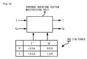
- FIG. 11 shows a configuration of the inverse rotating vector multiplying unit 5, which calculates equation (4).
- To generate the inverse rotating vector V' means to generate the values of a real part and an imaginary part of the vector, that is, to generate cos ⁇ ' and sin ⁇ ', where ⁇ is the phase of the inverse rotating vector V' in a manner that the vector on a complex plane rotates inversely.
- FIG. 11 shows a configuration of the inverse rotating vector multiplying unit 5, which calculates equation (4).
- FIG. 12 shows an I/Q table 60 on which pairs of cos ⁇ ' and sin ⁇ ' of a vector are arranged in order along the rotational direction of the vector, and the parameter output unit 6 is provided with the above-described I/Q table 60 in this example, addresses on the I/Q table 60 is read out at an increment or a decrement determined according to a set frequency of a designated voltage controlled oscillator 1, and is outputted to the inverse rotating vector multiplying unit 5. For instance, the addresses are read out one by one at the clock read-out timings from "0" to "11" and by returning to "0" again, the vector is to make one turn clockwise on a complex plane in 12 clocks. If the addresses are read at every other time by making the increment to be 2, the speed of the vector is doubled.
- the I/Q table 60 in FIG. 12 is diagrammatically prepared to make the understanding of the present embodiment easy, and it is not intended to list a preferable preparation example for the actual table.
- the frequency of the rotating vector V extracted from the carrier remove 4 is 40 MHz - (fvco/N) - 4 MHz.
- the set frequency of the voltage controlled oscillator 1 is fset, it is preferable for fset/N be close to 36 MHz as much as possible, and in this example, in the parameter output unit 6, an integer causing fset/N to be as close to 36 MHz as possible is operated, so that the integer is used as the frequency divider ratio N of the frequency divider.
- the frequency of the inverse rotating vector V' for stopping the rotating vector V extracted from the carrier remove 4 gets a value smaller than 4 MHz, and it is possible to generate the inverse rotating vector V' with small amount of data.
- the frequency after frequency division is 36 MHz as described above
- Such a calculation is conducted at the parameter output unit 6 before starting the voltage controlled oscillator 1 by inputting the set frequency to the frequency synthesizer.
- the parameter output unit 6 refers to a memory (not shown) and selects a voltage value with which a frequency close to the set frequency is obtained. Through this procedure, the output voltage of the voltage output unit 11 rises toward the voltage value.
- the frequency divider ratio N is set to 14
- the frequency of the inverse rotating vector V' is set to 1.1428642857143 MHz
- the output frequency fvco of the voltage controlled oscillator 1 is increased till the frequency of the frequency signal obtained at the A/D conversion unit 3 becomes 1.1428642857143 MHz.
- the frequency of the rotating vector V and the frequency of the inverse rotating vector V' are consistent with each other after a while, the PLL is locked and fvco converges to fset.
- FIG. 13 is a view showing a state that the rotating vector V is inversely processed by the inverse rotating vector V' and stopped in an image.
- the above-described operation is that in the case of stopping the rotating vector V relying on the inverse rotating vector V' only, and it is enough for this case to input a signal corresponding to the frequency of the rotating vector obtained at the inverse rotating vector multiplying unit 5 into a loop filter 8.
- an amount of data for generating the inverse rotating vector V' would be considerably great.
- the frequency of the rotating vector V is decelerated to a certain extent by the inverse rotating vector V', and the remaining reduction in speed is left to the operation of a time difference detection unit 71, an addition unit 72 and a cumulative addition unit 73 for phase difference at the subsequent stage.
- rough adjustment of the frequency of the rotating vector V is performed in the inverse rotating vector multiplying unit 5, and the rotating vector V is stopped by performing fine adjustment of the rotating vector V at parts in the subsequent stages.
- fb is 1 Hz
- m is 19, so that the adjustment worth of 19 Hz is executed by the part at the subsequent stage of the inverse rotating vector multiplying unit 5.
- 71 is the time difference detection unit for phases
- 72 is the second addition unit
- 73 is the cumulative addition unit 73 for phase differences
- 8 is the loop filter
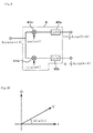
- 80 is the D/A (digital/analog) conversion unit. Since the rotation of the rotating vector V is reduced in speed by the inverse rotating vector V', it is possible to determine a frequency (speed) of the rotating vector V with a simple approximate expression. On a complex plane as shown in FIG.
- phase difference ⁇ is expressed by equation (5).
- imag is an imaginary part
- conj ⁇ V(n) ⁇ is a conjugate vector of V (n)
- K is a constant.
- ⁇ I I(n) - I(n - 1)
- ⁇ Q Q(n) - Q(n - 1).
- time difference detection unit 71 for phases is provided with a function to determine ⁇ using the approximate expression in this manner. Since this ⁇ is a value corresponding to the frequency of the rotating vector V reduced in speed by the inverse rotating vector multiplying unit 5, the time difference detection unit 71 for phases can be said to be a means (very slow speed vector detection means) outputting the frequency of the rotating vector reduced in speed.
- the parameter output unit 6 determines the value of 19Hz which is the amount corresponding to a frequency fine adjustment of the rotating vector V by calculation, the frequency of the rotating vector V detected at the time difference detection unit 71 for phases and 19Hz worthy of the fine adjustment are compared at the addition unit 72, and the difference between the frequency of the rotating vector V and 19Hz worthy of the fine adjustment is extracted, which is inputted into the cumulative addition unit 73.
- the output value from the cumulative addition unit 73 for phase differences is inputted into the loop filter 8.
- the frequency synthesizer performs a processing to stop the rotating vector V as shown in FIG. 8 .
- the processing is classified into rough suspension processing by so-called inverse rotation and processing to stop correctly the rotating vector V becoming a slow speed, and the latter processing is left to the time difference detection unit 71 for phases and the addition unit 72 in the example shown in FIG. 8 .
- the inverse rotating vector multiplying unit 5, the time difference detection unit 71 for phases and the second addition unit 72 correspond to a frequency difference extracting means.
- the cumulative addition unit 73 for phase differences is configured such that it stores an input value at the time of a certain sampling time to a resistor 73a as shown in FIG. 15A , outputs values stored till then at the time of next sampling to return them into the addition unit 73b for adding them to the input value, and the added value is inputted to the register 73a.
- the loop filter 8 is configured to cumulatively add the input value at a cumulative addition unit 8a and to add the input value to its cumulative addition value at an addition unit 8b.
- the reason to input the input value to the addition unit 8b is because the output of the loop filter 8 is stabilized.
- the output voltage of the loop filter 8 is converted into analog voltage at a D/A conversion unit 80, and is inputted into a first addition unit 12 so as to deduct the output voltage from the output voltage of the voltage output unit 11.
- a loop returning to the voltage controlled oscillation unit 1 from the voltage controlled oscillation unit via the frequency difference extracting means and the loop filter 8 forms a PLL.
- calculation processing of each part from the A/D converter 3 to the loop filter 8 is conducted by a software.
- a set frequency fset of the voltage controlled oscillator 1 is supposed to be, for instance, 520.0001 MHz, and is inputted from an input unit (not shown).
- the parameter output unit 6 is provided with a table in which a relation between a set frequency of the voltage controlled oscillator 1 and a supplied voltage is written, and a set frequency closest to 520.0001 MHz in this table is selected.
- the frequency divider ratio N 14 being an integer closest to fset/36 MHz, and the respective amounts obtained by dividing the frequency of the rotating vector V at the time the set frequency is obtained into a rough adjustment amount and a fine adjustment amount, are calculated.
- 1142883.30078125 Hz which is a rough adjustment amount of the frequency, in other words, the frequency of the inverse rotating vector, and the frequency 19 Hz of the rotating vector after inverse rotation processing which is a fine adjustment amount inputted into the second adder 72 are calculated.
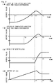
- the voltage corresponding to a set frequency is outputted from the voltage output unit 11 so as to rise linearly in relation to time for instance. Since voltage is supplied, the voltage controlled oscillator 1 outputs a frequency signal, and its frequency is increased. At the beginning, since the output frequency of the voltage controlled oscillator 1 is low, the frequency ⁇ 40 MHz - (output frequency/N) ⁇ extracted at the A/D conversion unit 3 is large, which makes the frequency of the rotating vector V extracted by the carrier remove 4 a negative large value, and the output of each unit after the carrier remove 4 is kept at a negative lowest level till the time 1. When the output frequency of the voltage controlled oscillator 1 rises to a certain value, the extracting calculation of the rotating vector V from the carrier remove 4 becomes effective so that the frequency (speed) of the rotating vector V starts decreasing (refer to FIG. 16A ).
- the output of the second addition unit 72 in other words, the input of the cumulative addition unit 73 for the phase differences is increased, the output of the cumulative addition unit 73 for the phase differences starts increasing at time t2 after time t1.
- the output frequency of the voltage controlled oscillator 1 is increased, the frequency after frequency division comes to 36 MHz, and it gets to the timing of stopping the speed of the rotating vector V extracted from the carrier remove 4.
- the frequency of the rotating vector V extracted from the carrier remove 4 is still smaller than the amount worthy of frequency adjustment ⁇ F + ⁇ f, and since its frequency difference (output of the second addition unit 72) is a negative value, the frequency of the rotating vector V is increased. Then, the frequency of the rotating vector V will be equal to the amount worthy of the above-described frequency adjustment ⁇ F + ⁇ f at the time of t3, but it is further increased according to the history of the PLL up to that time.
- the output of the time difference detection unit 71 for phases is finally converged to ⁇ f (in the above-described concrete example, it is 19 Hz) ( FIG. 16C ), and the output of the second addition unit 72, in other words, the frequency difference extracted by the frequency difference extracting means becomes zero.
- the PLL is locked, the output frequency of the voltage controlled oscillator 1 is locked to 520.0001 MHz, the set frequency.
- the loop filter 8 since the loop filter 8 has a complete integral function in this example, it converges to a positive direct current voltage.
- the time from starting the operation of the voltage controlled oscillator 1 till the PLL is locked is about 150 msec in simulation.
- the PLL is formed by extracting a rotating vector rotating at a speed (frequency) according to the output frequency of the voltage controlled oscillator 1, and by extracting the difference between the frequency of this rotating vector and the frequency of a rotating vector when the output frequency becomes a set frequency to feed it back to the voltage controlled oscillator 1, it is possible to perform a minute frequency setting over a wide frequency band at low noise. Then, at the time of extracting the frequency difference, the speed of the rotating vector is reduced using an inverse rotating vector inversely rotating at a rough frequency setting to detect the speed of the vector in its very slow speed rotation and by comparing its detected value with the amount of the fine adjustment calculated in advance, the difference is extracted. Accordingly, it is possible to detect the frequency of a rotating vector with a reduced data amount and with a simple calculation as described above, which makes it possible to configure a frequency synthesizer with a small memory size and small calculation load.
- the method of determining a frequency divider ratio N is not limited to the manner such that it is determined to be a frequency closest to a difference between the frequency of the reference clock signal used in the A/D conversion unit 3 and ⁇ 0 /2 ⁇ used in the rotating vector extracting means when the set value of an output frequency of the voltage controlled oscillator 1 is divided by N.
- a band noise generator 90 similar to that in embodiment 1 is provided, and this noise output is added to the output of the lowpass filter 21 in an adder 91 and this result is used as an analog input of the A/D converter 3.
- spurious generation due to a malfunction of the A/D converter 3 is reduced, and high performance at the frequency synthesizer can be realized.
Landscapes
- Engineering & Computer Science (AREA)
- Theoretical Computer Science (AREA)
- Stabilization Of Oscillater, Synchronisation, Frequency Synthesizers (AREA)
Applications Claiming Priority (2)
| Application Number | Priority Date | Filing Date | Title |
|---|---|---|---|
| JP2006100087 | 2006-03-31 | ||
| PCT/JP2007/057727 WO2007114523A1 (ja) | 2006-03-31 | 2007-03-30 | ディジタル処理装置 |
Publications (3)
| Publication Number | Publication Date |
|---|---|
| EP2003783A2 EP2003783A2 (de) | 2008-12-17 |
| EP2003783A9 true EP2003783A9 (de) | 2009-05-20 |
| EP2003783A4 EP2003783A4 (de) | 2011-03-09 |
Family
ID=38563781
Family Applications (1)
| Application Number | Title | Priority Date | Filing Date |
|---|---|---|---|
| EP07741163A Withdrawn EP2003783A4 (de) | 2006-03-31 | 2007-03-30 | Digitales verarbeitungsgerät |
Country Status (5)
| Country | Link |
|---|---|
| US (1) | US7764207B2 (de) |
| EP (1) | EP2003783A4 (de) |
| CN (1) | CN101416395B (de) |
| BR (1) | BRPI0709654A2 (de) |
| WO (1) | WO2007114523A1 (de) |
Families Citing this family (4)
| Publication number | Priority date | Publication date | Assignee | Title |
|---|---|---|---|---|
| KR100995173B1 (ko) * | 2006-03-31 | 2010-11-17 | 니혼 덴파 고교 가부시끼가이샤 | 주파수 신시사이저 |
| JP4787870B2 (ja) * | 2008-10-02 | 2011-10-05 | 日本電波工業株式会社 | 周波数シンセサイザ |
| FR3004035A1 (fr) * | 2013-03-26 | 2014-10-03 | Jacques Louis Marie Pontois | Dispositif et procede de synthese de frequence utilisant de multiples convertisseurs analogique numerique |
| KR20240056876A (ko) * | 2022-10-21 | 2024-05-02 | 연세대학교 산학협력단 | 확장된 정규 표현식 매칭 과정에서 nfa 자료 구조의 경량화를 위한 비트-패킹 방법, 이를 수행하는 장치 및 컴퓨터 프로그램 |
Family Cites Families (22)
| Publication number | Priority date | Publication date | Assignee | Title |
|---|---|---|---|---|
| JPH0634152Y2 (ja) * | 1988-12-08 | 1994-09-07 | 多機能カード | |
| JPH03283822A (ja) | 1990-03-30 | 1991-12-13 | Toshiba Corp | A/d変換装置 |
| JPH06132825A (ja) | 1992-10-16 | 1994-05-13 | Nippon Precision Circuits Kk | 信号生成回路 |
| SE505090C2 (sv) * | 1995-10-05 | 1997-06-23 | Ericsson Telefon Ab L M | Förfarande och anordning vid generering av en signal |
| US5903857A (en) * | 1996-11-18 | 1999-05-11 | Cirrus Logic, Inc. | Method and apparatus for calibrating an analog filter in a sampled amplitude read channel |
| JP3283822B2 (ja) | 1998-05-08 | 2002-05-20 | 賢親 鈴木 | ブレーキ装置付キャスタ |
| EP0961412B1 (de) * | 1998-05-29 | 2004-10-06 | Motorola Semiconducteurs S.A. | Frequenzsynthetisierer |
| US6157271A (en) * | 1998-11-23 | 2000-12-05 | Motorola, Inc. | Rapid tuning, low distortion digital direct modulation phase locked loop and method therefor |
| US6646386B1 (en) * | 1999-07-20 | 2003-11-11 | Tokyo Electron Limited | Stabilized oscillator circuit for plasma density measurement |
| US6268814B1 (en) | 2000-03-14 | 2001-07-31 | Lucent Technologies Inc. | Carrier-dependent dithering for analog-to-digital conversion |
| JP4652546B2 (ja) * | 2000-09-21 | 2011-03-16 | 三星電子株式会社 | 受信機 |
| US6512470B2 (en) * | 2001-01-05 | 2003-01-28 | Lite-On It Corp. | Method of voltage controlled oscillator digital/analog converted value adjustment of compact disk read only memory device |
| US6486810B1 (en) * | 2001-01-16 | 2002-11-26 | 3Com Corporation | Method and apparatus for continuously variable slope delta modulation coding of signals |
| JP2004104228A (ja) * | 2002-09-05 | 2004-04-02 | Matsushita Electric Ind Co Ltd | 信号処理装置および信号処理方法、デルタ・シグマ変調型分数分周pll周波数シンセサイザ、無線通信機器、デルタ・シグマ変調型d/a変換器 |
| US6834183B2 (en) * | 2002-11-04 | 2004-12-21 | Motorola, Inc. | VCO gain tracking for modulation gain setting calibration |
| US6924678B2 (en) * | 2003-10-21 | 2005-08-02 | Altera Corporation | Programmable phase-locked loop circuitry for programmable logic device |
| WO2006002844A1 (en) * | 2004-07-01 | 2006-01-12 | Ericsson Technology Licensing Ab | Apparatus comprising a sigma-delta modulator and method of generating a quantized signal in a sigma-delta modulator |
| KR100929084B1 (ko) * | 2004-12-03 | 2009-11-30 | 삼성전자주식회사 | 통신 시스템에서 디더링 장치 및 방법 |
| US7015853B1 (en) * | 2005-03-09 | 2006-03-21 | Cirrus Logic, Inc. | Data converter with reduced differential nonlinearity |
| US7224299B2 (en) * | 2005-09-30 | 2007-05-29 | Nxp, B.V. | System and method for adjusting dither in a delta sigma modulator |
| CN101421929B (zh) * | 2006-02-24 | 2011-11-30 | 日本电波工业株式会社 | Pll电路 |
| JP2008282506A (ja) * | 2007-05-14 | 2008-11-20 | Hitachi Ltd | 再生信号処理回路、再生信号処理方法及び光ディスクドライブ |
-
2007
- 2007-03-30 EP EP07741163A patent/EP2003783A4/de not_active Withdrawn
- 2007-03-30 CN CN2007800119023A patent/CN101416395B/zh not_active Expired - Fee Related
- 2007-03-30 BR BRPI0709654-2A patent/BRPI0709654A2/pt not_active IP Right Cessation
- 2007-03-30 WO PCT/JP2007/057727 patent/WO2007114523A1/ja not_active Ceased
- 2007-03-30 US US12/225,566 patent/US7764207B2/en active Active
Also Published As
| Publication number | Publication date |
|---|---|
| BRPI0709654A2 (pt) | 2011-07-19 |
| EP2003783A4 (de) | 2011-03-09 |
| WO2007114523A1 (ja) | 2007-10-11 |
| CN101416395B (zh) | 2011-03-16 |
| CN101416395A (zh) | 2009-04-22 |
| EP2003783A2 (de) | 2008-12-17 |
| US7764207B2 (en) | 2010-07-27 |
| US20090115652A1 (en) | 2009-05-07 |
Similar Documents
| Publication | Publication Date | Title |
|---|---|---|
| CN102291131B (zh) | 频率合成器 | |
| JP5006417B2 (ja) | Pll発振回路 | |
| US7764207B2 (en) | Digital processor | |
| US7642862B2 (en) | Digital phase locked loop | |
| US11588491B2 (en) | Signal generation circuit and method, and digit-to-time conversion circuit and method | |
| CN110518906A (zh) | 信号生成电路及其方法、数字时间转换电路及其方法 | |
| WO2008118659A1 (en) | Hardware and method to test phase linearity of phase synthesizer | |
| US8509296B2 (en) | Spectrum analyzer and spectrum analysis method | |
| WO2007049365A1 (ja) | 試験装置、クロック発生装置、及び電子デバイス | |
| US6377644B1 (en) | Periodic signal digital testing | |
| JP4299352B2 (ja) | ディジタル処理装置 | |
| EP2003779A9 (de) | Phasenregelkreiselement | |
| JP4397363B2 (ja) | 周波数シンセサイザ | |
| US8466724B2 (en) | Frequency synthesizer | |
| JP4606112B2 (ja) | 等間隔パルス列生成装置および生成方法 | |
| KR100980168B1 (ko) | 위상차 검출 장치 및 회전 위치 검출 장치 | |
| JP4874151B2 (ja) | ディジタル処理装置及び周波数シンセサイザ | |
| JP4713525B2 (ja) | 周波数シンセサイザ | |
| JP3201437B2 (ja) | 波形発生器のトリガ同期化回路 | |
| WO2004083875A1 (ja) | 検波装置、方法、プログラム、記録媒体 | |
| EP2330743A1 (de) | Frequenzsynthesizer | |
| JPH0697186B2 (ja) | 振動信号の解析装置 |
Legal Events
| Date | Code | Title | Description |
|---|---|---|---|
| PUAI | Public reference made under article 153(3) epc to a published international application that has entered the european phase |
Free format text: ORIGINAL CODE: 0009012 |
|
| 17P | Request for examination filed |
Effective date: 20080924 |
|
| AK | Designated contracting states |
Kind code of ref document: A2 Designated state(s): DE FR GB IT |
|
| PUAB | Information related to the publication of an a document modified or deleted |
Free format text: ORIGINAL CODE: 0009199EPPU |
|
| RBV | Designated contracting states (corrected) |
Designated state(s): DE FR GB IT |
|
| A4 | Supplementary search report drawn up and despatched |
Effective date: 20110204 |
|
| DAX | Request for extension of the european patent (deleted) | ||
| STAA | Information on the status of an ep patent application or granted ep patent |
Free format text: STATUS: THE APPLICATION HAS BEEN WITHDRAWN |
|
| 18W | Application withdrawn |
Effective date: 20130313 |