EP2005278B1 - Optoelektronische einrichtung zur bestimmung relativer bewegungen oder relativer positionen zweier objekte - Google Patents
Optoelektronische einrichtung zur bestimmung relativer bewegungen oder relativer positionen zweier objekte Download PDFInfo
- Publication number
- EP2005278B1 EP2005278B1 EP07724090A EP07724090A EP2005278B1 EP 2005278 B1 EP2005278 B1 EP 2005278B1 EP 07724090 A EP07724090 A EP 07724090A EP 07724090 A EP07724090 A EP 07724090A EP 2005278 B1 EP2005278 B1 EP 2005278B1
- Authority
- EP
- European Patent Office
- Prior art keywords
- light
- light shield
- optoelectronic device
- board
- relative
- Prior art date
- Legal status (The legal status is an assumption and is not a legal conclusion. Google has not performed a legal analysis and makes no representation as to the accuracy of the status listed.)
- Active
Links
Images






Classifications
-
- G—PHYSICS
- G06—COMPUTING OR CALCULATING; COUNTING
- G06F—ELECTRIC DIGITAL DATA PROCESSING
- G06F3/00—Input arrangements for transferring data to be processed into a form capable of being handled by the computer; Output arrangements for transferring data from processing unit to output unit, e.g. interface arrangements
- G06F3/01—Input arrangements or combined input and output arrangements for interaction between user and computer
- G06F3/03—Arrangements for converting the position or the displacement of a member into a coded form
- G06F3/033—Pointing devices displaced or positioned by the user, e.g. mice, trackballs, pens or joysticks; Accessories therefor
- G06F3/0354—Pointing devices displaced or positioned by the user, e.g. mice, trackballs, pens or joysticks; Accessories therefor with detection of two-dimensional [2D] relative movements between the device, or an operating part thereof, and a plane or surface, e.g. 2D mice, trackballs, pens or pucks
-
- G—PHYSICS
- G06—COMPUTING OR CALCULATING; COUNTING
- G06F—ELECTRIC DIGITAL DATA PROCESSING
- G06F3/00—Input arrangements for transferring data to be processed into a form capable of being handled by the computer; Output arrangements for transferring data from processing unit to output unit, e.g. interface arrangements
- G06F3/01—Input arrangements or combined input and output arrangements for interaction between user and computer
- G06F3/03—Arrangements for converting the position or the displacement of a member into a coded form
- G06F3/041—Digitisers, e.g. for touch screens or touch pads, characterised by the transducing means
- G06F3/042—Digitisers, e.g. for touch screens or touch pads, characterised by the transducing means by opto-electronic means
- G06F3/0421—Digitisers, e.g. for touch screens or touch pads, characterised by the transducing means by opto-electronic means by interrupting or reflecting a light beam, e.g. optical touch-screen
-
- G—PHYSICS
- G01—MEASURING; TESTING
- G01D—MEASURING NOT SPECIALLY ADAPTED FOR A SPECIFIC VARIABLE; ARRANGEMENTS FOR MEASURING TWO OR MORE VARIABLES NOT COVERED IN A SINGLE OTHER SUBCLASS; TARIFF METERING APPARATUS; MEASURING OR TESTING NOT OTHERWISE PROVIDED FOR
- G01D5/00—Mechanical means for transferring the output of a sensing member; Means for converting the output of a sensing member to another variable where the form or nature of the sensing member does not constrain the means for converting; Transducers not specially adapted for a specific variable
- G01D5/26—Mechanical means for transferring the output of a sensing member; Means for converting the output of a sensing member to another variable where the form or nature of the sensing member does not constrain the means for converting; Transducers not specially adapted for a specific variable characterised by optical transfer means, i.e. using infrared, visible, or ultraviolet light
- G01D5/32—Mechanical means for transferring the output of a sensing member; Means for converting the output of a sensing member to another variable where the form or nature of the sensing member does not constrain the means for converting; Transducers not specially adapted for a specific variable characterised by optical transfer means, i.e. using infrared, visible, or ultraviolet light with attenuation or whole or partial obturation of beams of light
- G01D5/34—Mechanical means for transferring the output of a sensing member; Means for converting the output of a sensing member to another variable where the form or nature of the sensing member does not constrain the means for converting; Transducers not specially adapted for a specific variable characterised by optical transfer means, i.e. using infrared, visible, or ultraviolet light with attenuation or whole or partial obturation of beams of light the beams of light being detected by photocells
-
- G—PHYSICS
- G01—MEASURING; TESTING
- G01L—MEASURING FORCE, STRESS, TORQUE, WORK, MECHANICAL POWER, MECHANICAL EFFICIENCY, OR FLUID PRESSURE
- G01L5/00—Apparatus for, or methods of, measuring force, work, mechanical power, or torque, specially adapted for specific purposes
- G01L5/16—Apparatus for, or methods of, measuring force, work, mechanical power, or torque, specially adapted for specific purposes for measuring several components of force
- G01L5/166—Apparatus for, or methods of, measuring force, work, mechanical power, or torque, specially adapted for specific purposes for measuring several components of force using photoelectric means
-
- G—PHYSICS
- G06—COMPUTING OR CALCULATING; COUNTING
- G06F—ELECTRIC DIGITAL DATA PROCESSING
- G06F3/00—Input arrangements for transferring data to be processed into a form capable of being handled by the computer; Output arrangements for transferring data from processing unit to output unit, e.g. interface arrangements
- G06F3/01—Input arrangements or combined input and output arrangements for interaction between user and computer
- G06F3/03—Arrangements for converting the position or the displacement of a member into a coded form
- G06F3/033—Pointing devices displaced or positioned by the user, e.g. mice, trackballs, pens or joysticks; Accessories therefor
- G06F3/0338—Pointing devices displaced or positioned by the user, e.g. mice, trackballs, pens or joysticks; Accessories therefor with detection of limited linear or angular displacement of an operating part of the device from a neutral position, e.g. isotonic or isometric joysticks
-
- G—PHYSICS
- G06—COMPUTING OR CALCULATING; COUNTING
- G06F—ELECTRIC DIGITAL DATA PROCESSING
- G06F3/00—Input arrangements for transferring data to be processed into a form capable of being handled by the computer; Output arrangements for transferring data from processing unit to output unit, e.g. interface arrangements
- G06F3/01—Input arrangements or combined input and output arrangements for interaction between user and computer
- G06F3/03—Arrangements for converting the position or the displacement of a member into a coded form
- G06F3/041—Digitisers, e.g. for touch screens or touch pads, characterised by the transducing means
- G06F3/042—Digitisers, e.g. for touch screens or touch pads, characterised by the transducing means by opto-electronic means
-
- G—PHYSICS
- G01—MEASURING; TESTING
- G01D—MEASURING NOT SPECIALLY ADAPTED FOR A SPECIFIC VARIABLE; ARRANGEMENTS FOR MEASURING TWO OR MORE VARIABLES NOT COVERED IN A SINGLE OTHER SUBCLASS; TARIFF METERING APPARATUS; MEASURING OR TESTING NOT OTHERWISE PROVIDED FOR
- G01D2205/00—Indexing scheme relating to details of means for transferring or converting the output of a sensing member
- G01D2205/95—Three-dimensional encoders, i.e. having codes extending in three directions
Definitions
- the present invention relates to an optoelectronic device for determining relative movements or relative positions of two objects.
- the invention also relates to a force and/or moment sensor incorporating such an optoelectronic device.
- the two- or three-dimensional displacements are detected by the peripheral device and described as a translation (X, Y, Z) and/or a rotation (A, B, C) in space. Furthermore, such displacements may be used to determine a corresponding applied force and/or moment.
- the optoelectronic device will typically include one or more measuring cell comprising a position-sensitive detector illuminated by a light-emitting element, such as a light emitting diode (LED), for measuring displacements in multiple (i.e. up to six degrees from freedom.
- a light-emitting element such as a light emitting diode (LED)
- Examples of such devices are known from United States Patent Application Publication No. 2003/102422 A1 and United States Patent Application Publication No. 2003/103217 A1 .
- US 2003102422 A1 discloses an optoelectronic arrangement for the detection of relative movements or relative positions of two objects.
- the arrangement comprises at least two position sensitive detectors, with each position sensitive detector being illuminated by a light emitting means in order to form a measuring cell.
- Each light emitting means illuminates two detectors, in order to form two measuring cells with a common light emitting means.
- a force and/or moment sensor is provided within this arrangement, with a first board and a second board, with the first board and the second board being elastically connected with each other and movable relative to one another.
- US 6 353 217 B1 discloses a transmitter receiver in which a light-shielding sheet is arranged in front of a light-emitting portion having a LED whose light-emitting central axis is inclined. An aperture from which only the head of the light-emitting portion is exposed is made in the light-shielding sheet.
- the light-shielding sheet masks the inclined side portion of the light-emitting portion to prevent a light-receiving portion from detecting the light leaking from the inclined side portion. Therefore, the light-receiving portion can detect with high accuracy a change in the amount of light emission that is produced by a change in the direction of the light-emitting portion.
- the present invention is based on the object of creating a more compact, more efficient and more easily assembled device design compared with known arrangements. That is, the design of the device is preferably more flexible and should require a smaller area. Also, the design of the device should be more economical to produce and should provide even more reliable operation. This design may then be implemented in the creation of an input device for use in The office or entertainment sectors or a force/moment sensor which allows uncomplicated input in up to six degrees-of-freedom.
- the present invention provides a light shield for an optoelectronic device as defined in the claims.
- the optoelectronic device of the invention is embodied as a force/moment sensor and is designed to function as an input device to allow uncomplicated and user-friendly motion input in up to six degrees-of-freedom in a 3D computer environment.
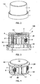
- the optoelectronic device 100 includes a frame or base 1 which typically remains stationary on a desktop or bench during use, and a knob-like cap 2 which is movably mounted on the base 1 and forms the input means with which a user may input movements to be detected and interpreted by the device 100.
- the cap 2 of the device 100 is designed to be grasped by the user and manipulated relative to the base 1 to generate the desired input.
- the lower edge of the cap is positioned in an annular recess 3 at the periphery of the base 1 with sufficient clearance to allow a degree of movement of the cap in all directions.
- the device 100 is thus designed to detect and ascertain or determine the movements or displacements of the cap 2 relative to the base 1.
- the optoelectronic device 100 includes a first board member 10 fixed relative to the base of the device, a second circular board member 20 resiliently mounted in spaced relation to the first board member 10 and adapted for movement or displacement relative thereto, and a plurality of optoelectronic measuring cells for determining relative movements or displacements between the first and second board members.
- the first and second board members 10, 20 are substantially rigid, plate-like members which preferably comprise a printed-circuit substrate and preferably also carry at least some of the electronic components of the optoelectronic measuring cells, as is known for example from US 2003/102422 and US 2003/103217 noted earlier.
- the first and second board members 10, 20 will simply be referred to as the first board 10 and the second board 20, respectively.
- the knob-like cap 2 is rigidly fixed to the second board 20 at an outer periphery thereof. That is, the second board 20 is fixed, e.g. using cement or adhesive, in abutment with a shoulder 4 formed on an inner surface of the cap 2. Furthermore, the first board 10 is rigidly connected to the frame or base 1, typically by means of screws inserted through mounting holes 5 formed in the base and through corresponding screw-holes 11 formed in the first board 10. Thus, the movement or position of the cap 2 relative to the base frame 1 is determined by detecting and measuring relative movements and/or positions of the first board 10 and the second board 20.
- the two 'objects' for which the optoelectronic device 100 of the invention determines relative movements or positions may be understood as being the first board 10 and the second board 20. Nevertheless, the relative movements or positions of those two objects also correspond to the relative movements or positions of the base 1 and the cap 2 to which the first board 10 and the second board 20 are respectively rigidly connected.
- the second board 20 is elastically connected to the first board 10 by three equally spaced coil spring elements 6.
- a lower end of each of the spring elements 6 is adapted to be received and fixed (preferably by soldering) within a corresponding mounting hole 12 formed in the first board 10.
- an upper end of each of the spring elements 6 is adapted to be received and fixed (again, preferably by soldering) within a corresponding mounting hole 22 formed in the second board 20.
- the substantially circular second board 20 is mounted in a neutral position (shown in Fig. 4 ) spaced directly above and essentially parallel to the substantially circular first board 10, such that the second board 20 is elastically biased to the neutral position by the spring elements 6.
- the springs 6 act to return the second board 20 to the neutral position when it is moved or displaced relative to the first board 10.
- each of the measuring cells for determining the relative movements and/or positions of the first and second boards 10, 20 comprises a light emitting element in the form of an infrared light-emitting diode (ILED) 13 projecting from on an upper side the first board 10 and a position-sensitive infrared detector (PSID) 23 mounted on an underside of the second board 20, facing the first board 10.
- ILED infrared light-emitting diode
- PSID position-sensitive infrared detector
- a light shield 30 is provided between the first board 10 and the second board 20 for effectively housing the ILEDs 13 and for shielding the PSIDs 23 from unwanted or extraneous light which might otherwise affect the accuracy of the readings the PSIDs provide.
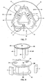
- the light shield 30 takes the form of a multi-sided (generally triangular) prismatic housing which is designed to be mounted stationary on the first board 10 such that it covers and substantially houses the ILEDs 13.
- Each PSID 23 is thereby designed to form a part of two separate measuring cells.
- the light shield 30 has a generally hollow structure with a number of cavities that define individual light-path channels 31 between each ILED 13 on the first board 10 and its respective PSID 23 mounted on the second board 20 above. Furthermore, as shown in Fig. 5 , the light shield housing 30 includes slit diaphragms 32 formed in a top side or wall 33 thereof, such that each of the slit diaphragms 32 is arranged in the light-path between one ILED 13 and the respective PSID 23 which that ILED is intended to illuminate.
- each of the ILEDs 13 is arranged in a vicinity of a vertex between two adjacent sides of the generally triangular housing 30 and the respective slit diaphragms 32 are centrally located along the lengths of each side at the top wall portion 33.
- the slit direction of each slit diaphragm 32 is substantially transverse, and preferably perpendicular, to a light-sensitive part or axis of the associated PSID 23.
- the wall portions 33 of the light shield 30 are non-transparent, i.e. typically opaque, to exclude unwanted or extraneous light from the PSIDs 23 and thereby ensure that only light transmitted through the slit diaphragms 32 falls upon the detectors.
- each of the PSIDs 23 is illuminated by two separate ILEDs 13 because each of the sides of the generally three-sided light shield housing 30 is divided into two separate light-path channels 31 by a central dividing wall 34.
- each PSID 23 is illuminated by its two separate ILEDs 13 via two separate slit diaphragms 32.
- Each of the slits 32 provides optical communication with the associated PSID for only one of the ILEDs 13. That is, each ILED 13 is provided with its own dedicated slit diaphragm 32.
- the slit diaphragms 32 of each pair are arranged substantially parallel and extend generally perpendicular to a light-sensitive part of the associated PSID 23.
- the two channels 31 formed along each side of the generally triangular housing 30 define converging light beam paths from the ILEDs 13 at the vertices towards the common PSID 23.
- the channels 31 of the light shield 30 thus define a plurality of individual light beam paths between the ILEDs 13 on the first board 10 and the PSIDs 23 on the second board 20, such that each of the light beam paths is arranged to extend at an angle in the range of about 30° to about 60° (and preferably at about 45°) relative to the plane of the first board 10, i.e. relative to a base reference plane for the device 100. Furthermore; the light beam paths defined by the light-path channels 31 formed along each side of the light shield 30 extend in three separate, intersecting planes generally corresponding to the planes of the sides of the housing 30.
- the light beam paths of the two measuring cells having a common PSID 23 may be considered to lie within the same plane, such that the light shield 30 forms a three-dimensional array of light beam paths between the ILEDs 13 and the PSIDs 23.
- This provides for a particularly compact optoelectronic device 100, while also affording great flexibility in modifications to the shape of the light shield.
- other light shield configurations including e.g. quadratic and pentagonal prisms and other multi-sided shapes, as well as curved sided shapes, are also contemplated by the present invention.
- the channels 31 on adjacent sides of the light shield housing 30 join with each other to form a V-shape recess at each of the corner regions, such that the light shield 30 has three V-shaped cavities or recesses separated from each other by the intermediate dividing walls 34.
- the pairs of ILEDs 13 arranged in each corner of the housing have relatively focussed light beams directed at their respective slit diaphragms 32 and PSIDs 23. This, together with the design and non-transparent nature of the light shield 30 itself, assists in ensuring that only light from an associated ILED 13 illuminates the respective PSID 23.
- each pair of ILEDs 13 mounted in each corner region of the light shield 30 could be replaced by a single ILED 13 having a broader beam.
- each ILED 13 could then illuminate both of the light-path channels 31 extending along adjacent sides of the housing, and thereby simultaneously illuminate two separate PSIDs 23.
- the optoelectronic device 100 further includes a stop arrangement 40 which is designed to provide a physical barrier to movement or displacement of the second board 20 relative to the first board 10 beyond a specific predetermined limit.
- the stop arrangement 40 thereby prevents any inadvertent overloading of the device 100 during use.
- the stop arrangement 40 comprises three generally elongate stop members 41 in the form of cylindrical studs or pins which are interconnected with one another at an upper end region thereof via a plate-like connecting member 42.
- the three pin members 41 are equally spaced apart from one another and extend substantially parallel from one side of the plate member 42.
- the pin members 41 are adapted to be received through corresponding openings or holes 24 formed through the second board 20 and to extend towards the base 1 to be rigidly secured relative thereto.
- the pin members 41 are arranged to align with the mounting holes 5 in the base 1 used for rigidly securing the first board 10. Accordingly, the pin members 41 are preferably also secured relative to the base 1 using the same mounting holes 5.
- the pin members 41 are preferably provided with an internally threaded bore at their end regions distal from the plate member 42.
- the distal ends of the pin members 41 could be secured to the first board 10 using an adhesive cement or other fastening means.
- the pin-like stop members 41 also form a mounting part 44 for fixing the stop arrangement 40 to the frame 1 of the optoelectronic device 100.
- the stop 40 has a generally robust and rigid structure for defining a solid limit to movement of the second board 20 relative to the first board 10.
- the pin members 41 and the rigid plate member 42 could conceivably be separately formed and pre-assembled as a sub-assembly of the optoelectronic device 100, the stop 40 is more preferably formed as a rigid unitary component, e.g. by injection molding using a relatively high-density polymer-plastics material.
- the openings or holes 24 formed through the second board 20 have a diameter substantially larger than the diameter of the pin members 41 they receive.
- each of the pin members 41 is positioned substantially centrally in its respective hole 24 through the second board.
- three elastomeric elements 7 in the form of rectangular foam blocks may be disposed between the first board 10 and the second board 20.
- the elastomeric blocks 7 may be attached to an underside of the second board 20 at positions closely adjacent to one of the pin members 41. In this way, as the second board 20 is displaced or moved such that an edge of the hole 24 approaches a point of contact with a lateral side of the respective pin member 41, the elastomeric block 7 is adapted to come into contact with the pin 41 and thereby dampen or cushion the contact between the second board 20 and the pin member of the stop.
- the foam blocks 7 may be mounted to extend from the second board 20 towards the first board 10, while terminating with a small gap between an end thereof and the first board. As the second board 20 is moved or displaced towards the first board 10, the elastomeric blocks 7 initially have no effect while the displacement is within the limits of the gap. Upon further displacement of the second board 20 towards the first board 10, however, the free end of at least one of the elastomeric blocks 7 comes into contact with the first board member 10 to cushion or dampen the movement of the second board 20 before it engages the stop 40.
- the foam blocks 7 may be mounted, e.g. adhered, to outer surfaces of the light shield 30 or may be mounted on the first board 10.
- the plate member 42 connecting the upper ends of the pin members 41 of the stop arrangement 40 comprises an annular peripheral region 43 where the surface is pitched at a specific predetermined angle relative to the neutral orientation angle of the second board 20 to thereby define a maximum angle of tilt of the second board 20 (and the cap 2) relative to the first board 10 (and the base frame 1) of the device.
- Such an angled annular peripheral region 43 may be provided on both an upper side and an underside of the plate member 42, as is apparent from Fig. 12 .
- a tilting (i.e. rotational) movement is applied to the second board 20 (via the cap 2) as shown, the second board 20 will deflect until, after a predetermined amount of tilting has occurred, the second board 20 engages the plate member 42 in the angled peripheral region 43.
- the contact or engagement with the angled peripheral surface region 43 of the fixed plate member 42 acts to stop further relative movement of the second board 20 in that direction.
- an upper inside surface of the cap 2 may engage a corresponding angled peripheral portion 43 of the plate member 42 as indicated in Fig. 12 .
- the first board 10, the light shield 30 and the stop 40 all remain stationary relative to the frame of the device 100, while the cap 2 and the second board 20 are moved relative thereto during operation of the device.
- FIG. 13 An alternative embodiment of an optoelectronic device according to the invention is schematically illustrated in Figs. 13 and 14 of the drawings.
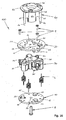
- An exploded view of the principle or core elements of this alternative embodiment of the device 100 is shown in Fig. 13 .
- This view generally corresponds to the exploded view shown in Fig. 1 , but with the base 1 and the cap 2 of the device omitted in this case.
- Like features of the optoelectronic device 100 corresponding to those features already described with reference to Fig. 1 to 12 are labeled with the same reference numerals.
- the embodiment of the optoelectronic device 100 in Figs. 13 and 14 of the drawings incorporates the same principles of the invention which are present in the previous embodiment, but in a somewhat different manner.
- the optoelectronic device 100 includes a first board 10 which is fixed to the base (not shown) and a second circular board 20 which is resiliently mounted on helical spring elements 6 in spaced and substantially parallel relation to the first board 10.
- the helical spring elements 6 are fixed to the first and second boards 10, 20 in the same manner as was described for the first embodiment, rendering the second board 20 resiliently movable relative to the first board 10 about a neutral position.
- the optoelectronic device has a plurality of measuring cells, each of which comprises an ILED 13 and a PSID 23.
- the ILEDs 13 are mounted on the second board 20 for movement relative to the first board 10
- the PSIDs 23 are mounted on the first board 10 facing the ILEDs 13 and are fixed relative to the frame of the device.
- the optoelectronic device 100 of this embodiment has six measuring cells arranged in three groups, such that pairs of the ILEDs 13 are directed to illuminate a common PSID 23.
- the light shield 30 in this embodiment has quite a different configuration to the generally prismatic shape in the first embodiment, but certain characteristic features remain unchanged.
- the light shield 30 still has a roughly triangular configuration and includes two individual light-path channels 31 formed at each of the three side regions of that triangular configuration. In this case, however, rather than being defined by the parallel walls of a prismatic housing, the light-path channels 31 are formed in separate or discrete compartments 35 attached at the sides of the integral light shield component 30.
- Each of the compartments 35 has a pod-like structure, the wall portions 33 of which surround and enclose two individual channels 31 which are separated from each other by a central by dividing wall portion 34.
- each compartment 35 defines a pair of cavities forming light-path channels 31 which extend downwardly from the second board 20 towards the first board 10 for directing or guiding light from the respective ILEDs 13 to a PSID 23.
- each channel 31 receives and partially houses one of the ILEDs 13. Note that, because the ILEDs 13 have relatively focused light beams, a full enclosure or full housing of each ILED 13 within the light shield 30 is not necessary.
- the light paths defined by the pair of channels 31 for the ILEDs 13 which illuminate a common PSID 23 i.e. the channels 31 in each of the pod-like compartments 35 in this case
- the light beam paths defined by the channels 31 at each side of the light shield 30 extend in separate, intersecting planes such that the light shield 30 forms a three-dimensional array of light beam paths between the ILEDs 13 and the PSIDs 23.
- the light shield 30 of this second embodiment can be seen in more detail in Fig. 15 , albeit with some minor modifications compared with the schematic version shown in Fig. 13 .
- the upper part of the side wall portions 33 of each pod-like compartment 35 forming the light-path channels 31 are not cut away, such that each of the ILEDs 13 in this light shield 30 will be substantially fully enclosed and housed within a respective channel of the light shield when the device 100 is assembled.
- the wall portions of the light shield 30 on an underside of each of the pod-like compartments 35 incorporates slit diaphragms 32 above each of the PSIDs 23 in the same way as slit diaphragms were incorporated into the light shield housing in the first embodiment.
- the light shield component 30 in this embodiment is designed to be securely fixed to, and thus suspended from, the movable second board 20 for movement therewith relative to the first board member 10.
- Fig. 15 shows screw holes 36 formed adjacent the dividing wall portion 34 between each of the channels 31 in the pod-like compartments 35 for screw-fastening the light shield 30 to the second board 20.
- the PSIDs 23 of the optoelectronic device 100 fixed on the fist board member 10 detect movements and positions of the second board 20 by detecting light transmitted from the movable ILEDs 13 and illuminating the PSIDs 23 via the slit diaphragms 32 formed in the underside of the pod-like structures 35.
- the light shield 30 of this second embodiment constitutes a multi-function component of the optoelectronic device 100. That is, its function is not merely to direct or guide light to the PSIDs 23 in such a way that they are shielded from extraneous or unwanted light.
- the light shield component 30 also has a mounting capacity for connection to the second board 20 via screw holes 36.
- the light shield component 30 incorporates a central space or cavity 37 which is designed to receive the stop arrangement 40, and in particular, the elongate stop members 41.
- the light shield 30 could incorporate three cylindrical spaces or cavities for a stop arrangement 40 having the same configuration as in the first embodiment.
- the stop arrangement 40 has a somewhat different configuration (as described in more detail below) and as a result, the space or cavity 37 is continuous.
- the previous circular openings 24 formed in the second board 20 for accommodating the pin members 41 of the stop arrangement 40 have been interconnected in this embodiment to form a single continuous opening 25 with portions of the circular openings 24 still in the corners.
- an edge region of the light shield component 30 may be shaped to match the opening 25 formed in the board 20 to facilitate positioning and mounting of the light shield. In this regard, as can be seen in Fig.
- an upper edge region of the light shield component 30 has an upstanding rim 38, the outer profile of which is designed to match the shape of the opening 25 formed in the second board 20.
- the rim 38 can be fittingly received within the opening 38 when the light shield component 30 is attached to the second board 20.
- the space or cavity 37 in the light shield component 30 includes a central region for receiving a mounting part of the stop arrangement 40 and lobes extending therefrom for receiving the respective stop members 41, as noted below.
- the stop 40 comprises a central mounting part 44 in the form of an elongate cylindrical member which is designed to be fixed relative to a frame of the optoelectronic device at a lower end thereof.
- a large screw fastener 8 is provided which passes through the central screw hole 14 formed in the first board 10 and which engages a correspondingly threaded bore (not shown) in the central mounting part 44.
- the same screw fastener 8 may also rigidly secure the first board 10 to the base or frame of the optoelectronic device 100. (See Fig. 1 ).
- the stop arrangement 40 comprises three elongate stop members 41 in the form of generally cylindrical pin- or stud-members, as was the case in the first embodiment. These stop members 41 are arranged laterally of and spaced around the central mounting part 44. Furthermore, the stop members 41 extend substantially parallel to the mounting part 44 and to one another. As was also the case in the first embodiment, the stop arrangement 40 incorporates a disc-shaped plate member 42 which rigidly interconnects an upper end of each of the stop members 41 with one another. Importantly, this plate member 42 also rigidly connects each of the stop members 41 with an upper end region of the cylindrical mounting member 44 - that is, the end region of the mounting part 44 which is opposite the lower end region that is fixed to the frame of the device with the screw fastener 8.
- a connection between the stop members 41 and the mounting part 44 is also effected by web elements 45 which extend radially outward from the central mounting part 44 towards the stop members.
- Such radial webs, fins or rib elements enhance the rigidity of the stop arrangement 40 and in particular serve to stabilize the elongate stop members 41.
- the thickness of the web elements 45 can be selected according to the degree of rigidity required.
- the web elements 45 are shown to extend over substantially the entire length of the stop members 41, but this too may be altered according to the degree of rigidity required.
- the elongate stop members 41 have substantially the same length as the central mounting member 44, such that the lower ends of the stop members 41 extend to the first board 10. Unlike the first embodiment, however, these lower end regions of the stop members 41 are not fixed to the first board 10. Rather, the lower end regions of the stop members 41 merely contact and bear against the upper surface of the first board. In this way, the stop 40 of this embodiment is able to be mounted and secured to the frame by a single fastening operation via the screw fastener 8 secured to the mounting part 44.
- stop members 41 it will be understood by persons skilled in the art that it is not necessary that the stop members 41 be particularly long nor that they extend from the plate member 42 to the first board 10.
- the central mounting part 44 is responsible for rigidly fixing the stop arrangement 40 to the frame of the device 100 at its lower end region, the stop members 41 do not need to contact the first board at all (although such a configuration may provide enhanced stability).
- the stop members 41 need only extend an amount sufficient to interact with the second board member 20 and/or with the upper rim 38 or an upper wall portion of the light shield component 30 forming the cavity 37 which receives the stop members 41.
- FIG. 16 and 17 of the drawings a more detailed illustration of an embodiment of the optoelectronic device of the invention corresponding to the schematic illustrations in Figs. 13 and 14 is provided.
- These drawings show more detail, but like features are labeled with corresponding reference numerals.
- the plate connecting member 42 of the stop arrangement 40 has an angled peripheral region 43 having the same design and function as that described with reference to Figs. 8 to 12 .
- each stop member 41 includes a small projection 46 which is designed to be received and located in a respective hole 15 formed in the first board member 10.
- the lower ends of the stop members 41 having the projection 46 are not fixed to the first board member 10, but are merely inserted into the holes 15 to properly position or register the stop member 40.
- the interaction between the projections 46 and the holes 15 also provides the stop members 41 with enhanced stability when a lateral rotation of the second board 20 (i.e. via the cap 2) - e.g. as illustrated in Fig. 10 - brings the board into contact with the stop members 41.
- FIG. 16 and 17 A further detail of the embodiment shown in Figs. 16 and 17 relates to a functional aspect of the light shield component 30 not previously described with reference to Figs. 13 and 14 .
- This further functional aspect relates to the provision of small nodules or rounded projections (not shown) on an underside of the light shield component 30 at locations between the three PSIDs 23 mounted on the first board 10.
- These nodules or rounded projections are designed to act as stop elements to prevent the light shield component 30 from inadvertently coming into contact with the PSIDs 23 in the event that the second board 20 is pressed downwardly against the bias of the helical spring elements 6 before the cap 2 is attached to the optoelectronic device 100.
- Fig. 16 and 17 A further detail of the embodiment shown in Figs. 16 and 17 relates to a functional aspect of the light shield component 30 not previously described with reference to Figs. 13 and 14 .
- This further functional aspect relates to the provision of small nodules or rounded projections (not
- the plate-like connecting member 42 typically interacts with the cap 2 to limit the range of downward movement of the second board.
- the nodules or rounded projections (not shown) on the underside of the light shield component 30 provide a clearance above the level of the PSIDs 23 to ensure that the sensitive PSID components 23 cannot be damaged by an inadvertent depression of the second board 20 prior to attachment of the cap 2.
- the PSIDs 23 are typically mounted and electrically connected by wire elements soldered to the first board 10, while each of the ILEDs 13 is typically correspondingly mounted and electrically connected by wire elements soldered to the movable second board 20.
- the light shield component 30 is rigidly secured to the second board 20 by fastening screws 9 which pass through holes 26 in the second and engage into the holes 36 after the upper rim has been mated or fittingly received in the matching opening 25 provided in the second board 20.
- the provision of lugs or projections 39 e.g. on the rim 38
- corresponding recesses or indentation in the opening 25 in board 20 further assists to properly locate the light shield component 30 relative to the board 20 and ensure that the respective orientation of the parts is correct.
Landscapes
- Engineering & Computer Science (AREA)
- General Engineering & Computer Science (AREA)
- Theoretical Computer Science (AREA)
- Physics & Mathematics (AREA)
- General Physics & Mathematics (AREA)
- Human Computer Interaction (AREA)
- Length Measuring Devices By Optical Means (AREA)
- Switches Operated By Changes In Physical Conditions (AREA)
Claims (16)
- Lichtabschirmelement (30) für eine optoelektronische Vorrichtung (100), die relative Bewegungen oder relative Positionen von zwei Objekten, umfassend ein erstes Objekt und ein zweites Objekt, bestimmt, wobei das Lichtabschirmelement (30) eine Mehrzahl von Kanälen (31) umfasst, von denen jeder einen Strahlengang für einen Lichtstrahl zwischen einem lichtemittierenden Element (13) und einem Detektor (23) der optoelektronischen Vorrichtung bildet, dadurch gekennzeichnet, dass das Lichtabschirmelement eine im Wesentlichen hohle Struktur mit einer Anzahl von Hohlräumen hat, die individuelle Strahlengangkanäle (31) zwischen jedem lichtemittierenden Element (13) und dem zugehörigen Detektor (23) bilden, und dass mindestens zwei der Kanäle (31) Strahlengänge definieren, die von den lichtemittierenden Elementen (13) zu dem zugehörigen Detektor (23) hin miteinander konvergieren.
- Lichtabschirmelement (30) nach Anspruch 1, wobei die Mehrzahl von Strahlengangkanälen (31) in einer oder mehreren Gruppen von mindestens zwei angeordnet ist und separate Strahlengänge definiert, die zu einem gemeinsamen Detektor (23) hin konvergieren.
- Lichtabschirmelement (30) nach Anspruch 1, wobei die Mehrzahl von Kanälen (31) gemeinsam eine nicht-planare oder dreidimensionale Anordnung von Strahlengängen zwischen dem ersten und dem zweiten Objekt (10, 20) der optoelektronischen Vorrichtung definiert und/oder wobei die Mehrzahl von Kanälen (31) vorzugsweise so angeordnet ist, dass sich die von den Kanälen (31) definierten Strahlengänge in separaten Ebenen, vorzugsweise sich schneidenden Ebenen, zwischen dem ersten und dem zweiten Objekt erstrecken.
- Lichtabschirmelement (30) nach Anspruch 1, wobei das zweite Objekt (20) im Wesentlichen flach ist und im Wesentlichen parallel beabstandet zu dem ersten Objekt (10) angebracht ist, wobei das Lichtabschirmelement (30) zwischen dem ersten Objekt (10) und dem zweiten Objekt (20) angebracht zu werden vermag.
- Lichtabschirmelement (30) nach einem der Ansprüche 1 bis 4, wobei die Kanäle (31) von Wandteilen (33, 34) des Lichtabschirmelements (30) gebildet werden und wobei jeder Kanal den Strahlengang mindestens teilweise umgibt oder umschließt, um einen Hohlraum zu definieren, an dem entlang das Licht zwischen einem lichtemittierenden Element (13) und einem Detektor (23) der optoelektronischen Vorrichtung geleitet oder geführt wird.
- Lichtabschirmelement (30) nach Anspruch 5, wobei das Lichtabschirmelement (30) lichtemittierende Elemente (13) der optoelektronischen Vorrichtung mindestens teilweise zu umschließen oder aufzunehmen vermag und/oder ferner eine oder mehrere Schlitzblenden (32) in den Wandteilen (33, 34) umfasst, die die Kanäle (31) umschließen.
- Lichtabschirmelement (30) nach einem der Ansprüche 1 bis 6, wobei die Strahlengangkanäle (31) Strahlengänge definieren, die in einem Winkel relativ zu einer Bezugsebene geneigt sind, die einer Ebene des Rahmens der Vorrichtung und/oder einer Ebene des ersten Objekts (10) entspricht, und/oder wobei die Strahlengangkanäle (31) vorzugsweise Lichtstrahlengänge definieren, die in einem Winkel zwischen 0° und 90° relativ zu der Bezugsebene, vorzugsweise in einem Winkel im Bereich von 0° bis 60° und noch bevorzugter in einem Winkel im Bereich von 10° bis 30° geneigt sind.
- Lichtabschirmelement (30) nach einem der Ansprüche 1 bis 7, wobei das Lichtabschirmelement (30) als eine einheitliche oder integrale Komponente gebildet ist und vorzugsweise ferner einen Raum oder Hohlraum (35) umfasst, der eine Anschlaganordnung (40) oder mindestens ein Anschlagelement (41) der optoelektronischen Vorrichtung (100) aufzunehmen vermag, wobei Wandteile (36) des Lichtabschirmelements, die den Raum oder Hohlraum (35) definieren, vorzugsweise bei einer Grenze der relativen Bewegung zwischen dem ersten Objekt (10) und dem zweiten Objekt (20) mit der Anschlaganordnung (40) oder dem mindestens einen Anschlagelement (41) in Kontakt zu kommen vermögen.
- Lichtabschirmelement (30) nach Anspruch 8, wobei die Strahlengangkanäle (31) um den Raum oder Hohlraum (35) zum Aufnehmen der Anschlaganordnung (40) oder des mindestens einen Anschlagelements (41) herum angeordnet sind und/oder wobei das Lichtabschirmelement (30) entweder an dem ersten Objekt (10) oder an dem zweiten Objekt (20) angebracht zu werden vermag.
- Optoelektronische Vorrichtung (100) zum Bestimmen von relativen Bewegungen oder relativen Positionen von zwei Objekten, umfassend:ein erstes Objekt (10), das relativ zu einem Rahmen (1) der Vorrichtung befestigt ist;ein zweites Objekt (20), das beabstandet zu dem ersten Objekt (10) angebracht ist und sich relativ dazu zu bewegen vermag;eine Mehrzahl von Messzellen zum Bestimmen von Bewegung oder Verschiebung des zweiten Objekts (20) relativ zu dem ersten Objekt (10), wobei jede Messzelle ein lichtemittierendes Element (13) und einen Detektor (23) zum Detektieren von Licht von dem lichtemittierenden Element (13) umfasst; undein Lichtabschirmelement (30) nach einem der vorhergehenden Ansprüche, das zwischen dem ersten Objekt und dem zweiten Objekt angebracht ist, wobei sich jeder Strahlengangkanal (31) des Lichtabschirmelements (30) mindestens über einen Teil der Entfernung zwischen einem lichtemittierenden Element (13) und einem Detektor (23) einer der Messzellen erstreckt.
- Optoelektronische Vorrichtung (100) nach Anspruch 10, wobei jede Messzelle ferner eine Schlitzblende (32) umfasst, die in dem Strahlengang zwischen dem positionsempfindlichen Detektor (23) und dem lichtemittierenden Element (13) angeordnet ist, wobei das Lichtabschirmelement (30) die Schlitzblende (32) in einem Seiten- oder Wandteil (33, 34) davon enthält und wobei sich vorzugsweise jeder von dem Lichtabschirmelement (30) definierte Strahlengangkanal (31) zwischen einem lichtemittierenden Element (13) und einer zugehörigen Schlitzblende (32) erstreckt.
- Optoelektronische Vorrichtung (100) nach einem der Ansprüche 10 oder 11, wobei mindestens ein Detektor (23) von zwei separaten lichtemittierenden Elementen (13) angestrahlt wird, um dadurch zwei Messzellen mit einem gemeinsamen Detektor zu bilden, wobei das Lichtabschirmelement (30) separate Strahlengangkanäle (31) definiert, die sich zwischen den separaten lichtemittierenden Elementen (13) und dem gemeinsamen positionsempfindlichen Detektor (23) erstrecken, und wobei vorzugsweise jede der zwei Messzellen mit dem gemeinsamen Detektor (23) eine separate Schlitzblende (32) hat, die in dem Strahlengang des entsprechenden lichtemittierenden Elements (13) angeordnet ist, wobei die separaten Schlitzblenden (32) in einem Seiten- oder Wandteil (33, 34) des Lichtabschirmelements (30) einander benachbart, vorzugsweise parallel, angeordnet sind oder wobei jeder Detektor (23), der von mehr als einem lichtemittierenden Element (13) angestrahlt wird, um mehrere Messzellen zu bilden, abwechselnd (d.h. periodisch) von den lichtemittierenden Elementen angestrahlt wird.
- Optoelektronische Vorrichtung (100) nach einem der Ansprüche 10 bis 12, wobei eine Anschlaganordnung (40) oder mindestens ein Anschlagelement (41) in einem Raum oder Hohlraum (35) des Lichtabschirmelementes (30) aufgenommen wird, um eine Bewegung des zweiten Objekts (20) relativ zu dem ersten Objekt (10) zu begrenzen.
- Optoelektronische Vorrichtung (100) nach Anspruch 13, wobei Wandteile (36) des Lichtabschirmelements (30), die den Raum oder Hohlraum (35) definieren, bei einer Grenze der relativen Bewegung zwischen dem ersten Objekt (10) und dem zweiten Objekt (20) mit der Anschlaganordnung (40) oder dem mindestens einen Anschlagelement (41) in Kontakt zu kommen vermögen, oder wobei die Strahlengangkanäle (31) in dem Lichtabschirmelement (30) um den Raum oder Hohlraum (35) zum Aufnehmen der Anschlaganordnung (40) oder des Anschlagelements (41) herum angeordnet sind.
- Kraft- und/oder Momentensensor, der eine optoelektronische Vorrichtung (100) nach einem der Ansprüche 10 bis 14 enthält.
- Tastatur für einen Personalcomputer, die eine optoelektronische Vorrichtung (100) nach einem der Ansprüche 10 bis 14 enthält.
Priority Applications (1)
| Application Number | Priority Date | Filing Date | Title |
|---|---|---|---|
| EP07724090A EP2005278B1 (de) | 2006-04-05 | 2007-04-05 | Optoelektronische einrichtung zur bestimmung relativer bewegungen oder relativer positionen zweier objekte |
Applications Claiming Priority (3)
| Application Number | Priority Date | Filing Date | Title |
|---|---|---|---|
| EP06007195A EP1843243B1 (de) | 2006-04-05 | 2006-04-05 | Optoelektronische Vorrichtung zur Bestimmung der relativen Bewegungen oder relativen Positionen zweier Objekte |
| EP07724090A EP2005278B1 (de) | 2006-04-05 | 2007-04-05 | Optoelektronische einrichtung zur bestimmung relativer bewegungen oder relativer positionen zweier objekte |
| PCT/EP2007/003149 WO2007115812A2 (en) | 2006-04-05 | 2007-04-05 | Optoelectronic device for determining relative movements or relative positions of two objects |
Publications (2)
| Publication Number | Publication Date |
|---|---|
| EP2005278A2 EP2005278A2 (de) | 2008-12-24 |
| EP2005278B1 true EP2005278B1 (de) | 2012-08-15 |
Family
ID=36968913
Family Applications (4)
| Application Number | Title | Priority Date | Filing Date |
|---|---|---|---|
| EP06007195A Expired - Lifetime EP1843243B1 (de) | 2006-04-05 | 2006-04-05 | Optoelektronische Vorrichtung zur Bestimmung der relativen Bewegungen oder relativen Positionen zweier Objekte |
| EP07007527A Expired - Lifetime EP1850210B1 (de) | 2006-04-05 | 2006-04-05 | Optoelektronische Vorrichtung zur Bestimmung der relativen Bewegungen oder relativen Positionen zweier Objekte |
| EP07724087A Withdrawn EP2005277A2 (de) | 2006-04-05 | 2007-04-05 | Optoelektronische einrichtung zur bestimmung relativer bewegungen oder relativer positionen zweier objekte |
| EP07724090A Active EP2005278B1 (de) | 2006-04-05 | 2007-04-05 | Optoelektronische einrichtung zur bestimmung relativer bewegungen oder relativer positionen zweier objekte |
Family Applications Before (3)
| Application Number | Title | Priority Date | Filing Date |
|---|---|---|---|
| EP06007195A Expired - Lifetime EP1843243B1 (de) | 2006-04-05 | 2006-04-05 | Optoelektronische Vorrichtung zur Bestimmung der relativen Bewegungen oder relativen Positionen zweier Objekte |
| EP07007527A Expired - Lifetime EP1850210B1 (de) | 2006-04-05 | 2006-04-05 | Optoelektronische Vorrichtung zur Bestimmung der relativen Bewegungen oder relativen Positionen zweier Objekte |
| EP07724087A Withdrawn EP2005277A2 (de) | 2006-04-05 | 2007-04-05 | Optoelektronische einrichtung zur bestimmung relativer bewegungen oder relativer positionen zweier objekte |
Country Status (6)
| Country | Link |
|---|---|
| US (2) | US8243024B2 (de) |
| EP (4) | EP1843243B1 (de) |
| JP (1) | JP5155996B2 (de) |
| KR (1) | KR20090006072A (de) |
| CN (1) | CN101410776B (de) |
| WO (2) | WO2007115812A2 (de) |
Families Citing this family (64)
| Publication number | Priority date | Publication date | Assignee | Title |
|---|---|---|---|---|
| EP1998243A1 (de) | 2007-05-25 | 2008-12-03 | 3Dconnexion Holding SA | Optoelektronische Vorrichtung und elastisches Element dafür |
| GB2462081A (en) * | 2008-07-21 | 2010-01-27 | Eigenlabs Ltd | A programmable sound creation interface |
| EP2255935B1 (de) * | 2009-05-28 | 2012-06-20 | Max Co., Ltd. | Elektrisches Heftgerät |
| JP2011065409A (ja) * | 2009-09-17 | 2011-03-31 | Seiko Epson Corp | 光学式位置検出装置および位置検出機能付き表示装置 |
| JP5493674B2 (ja) * | 2009-10-13 | 2014-05-14 | セイコーエプソン株式会社 | 光検出器、光学式位置検出装置および位置検出機能付き表示装置 |
| TW201139997A (en) * | 2010-05-05 | 2011-11-16 | Edison Opto Corp | Partition type optical sensing device |
| JP2014052664A (ja) * | 2010-12-22 | 2014-03-20 | Sony Computer Entertainment Inc | 操作子及び操作装置 |
| US8785012B2 (en) | 2011-06-09 | 2014-07-22 | Bloom Energy Corporation | Fuel cell bypass diode structures and attachment methods |
| WO2014164207A1 (en) | 2013-03-12 | 2014-10-09 | Stryker Corporation | Sensor assembly and method for measuring forces and torques |
| KR102095013B1 (ko) * | 2013-04-11 | 2020-03-31 | 삼성디스플레이 주식회사 | 플렉서블 장치 |
| JP6402719B2 (ja) * | 2013-11-05 | 2018-10-10 | 日本精工株式会社 | 力覚センサ |
| JP2015197357A (ja) * | 2014-04-01 | 2015-11-09 | キヤノン株式会社 | 光学式力角センサおよびこれを用いた装置 |
| DE102014216389A1 (de) * | 2014-08-19 | 2016-02-25 | BSH Hausgeräte GmbH | Bedienvorrichtung für ein Haushaltsgerät mit stabil positioniertem ringförmigen Bedienelement-Vorderteil und Haushaltsgerät mit einer derartigen Bedienvorrichtung |
| US11397108B2 (en) * | 2015-06-16 | 2022-07-26 | Marquardt Gmbh | Multi-function controller and method of using same |
| US10239213B1 (en) * | 2015-11-24 | 2019-03-26 | X Development Llc | Flexure assembly for force/torque sensing |
| JP6575334B2 (ja) * | 2015-12-01 | 2019-09-18 | 日本精工株式会社 | 力覚センサ |
| US10274386B2 (en) | 2016-06-20 | 2019-04-30 | X Development Llc | Retroreflective multi-axis force torque sensor |
| US10732061B2 (en) | 2017-09-07 | 2020-08-04 | X Development Llc | Unibody flexure design for displacement-based force/torque sensing |
| US11428589B2 (en) * | 2017-10-16 | 2022-08-30 | Saf-Holland, Inc. | Displacement sensor utilizing ronchi grating interference |
| US10637470B2 (en) * | 2018-01-05 | 2020-04-28 | Darfon Electronics Corp. | Optical keyswitch |
| CN108490630B (zh) * | 2018-03-12 | 2019-10-22 | Oppo广东移动通信有限公司 | 激光投射模组、深度相机和电子装置 |
| WO2019165862A1 (zh) | 2018-02-27 | 2019-09-06 | Oppo广东移动通信有限公司 | 激光投射模组、深度相机和电子装置 |
| CN108508687B (zh) * | 2018-03-12 | 2021-06-18 | Oppo广东移动通信有限公司 | 激光投射模组、深度相机和电子装置 |
| CN108490572B (zh) * | 2018-03-12 | 2021-04-23 | Oppo广东移动通信有限公司 | 激光投射模组、深度相机及电子装置 |
| US11559298B2 (en) | 2018-07-16 | 2023-01-24 | Cilag Gmbh International | Surgical visualization of multiple targets |
| US10732060B2 (en) | 2018-08-15 | 2020-08-04 | X Development Llc | Force/torque sensor with hardstops to limit overloading a flexure |
| US11213361B2 (en) | 2019-03-15 | 2022-01-04 | Cilag Gmbh International | Robotic surgical systems with mechanisms for scaling surgical tool motion according to tissue proximity |
| US11284957B2 (en) | 2019-03-15 | 2022-03-29 | Cilag Gmbh International | Robotic surgical controls with force feedback |
| US11490981B2 (en) | 2019-03-15 | 2022-11-08 | Cilag Gmbh International | Robotic surgical controls having feedback capabilities |
| US11471229B2 (en) | 2019-03-15 | 2022-10-18 | Cilag Gmbh International | Robotic surgical systems with selectively lockable end effectors |
| EP3937818A1 (de) | 2019-03-15 | 2022-01-19 | Cilag GmbH International | Eingabesteuerungen für roboterchirurgie |
| US11992282B2 (en) | 2019-03-15 | 2024-05-28 | Cilag Gmbh International | Motion capture controls for robotic surgery |
| US11666401B2 (en) | 2019-03-15 | 2023-06-06 | Cilag Gmbh International | Input controls for robotic surgery |
| WO2020188391A1 (en) | 2019-03-15 | 2020-09-24 | Ethicon Llc | Robotic surgical controls having feedback capabilities |
| US11690690B2 (en) | 2019-03-15 | 2023-07-04 | Cilag Gmbh International | Segmented control inputs for surgical robotic systems |
| US12257013B2 (en) | 2019-03-15 | 2025-03-25 | Cilag Gmbh International | Robotic surgical systems with mechanisms for scaling camera magnification according to proximity of surgical tool to tissue |
| US11583350B2 (en) | 2019-03-15 | 2023-02-21 | Cilag Gmbh International | Jaw coordination of robotic surgical controls |
| US11219501B2 (en) | 2019-12-30 | 2022-01-11 | Cilag Gmbh International | Visualization systems using structured light |
| US12207881B2 (en) | 2019-12-30 | 2025-01-28 | Cilag Gmbh International | Surgical systems correlating visualization data and powered surgical instrument data |
| US11744667B2 (en) | 2019-12-30 | 2023-09-05 | Cilag Gmbh International | Adaptive visualization by a surgical system |
| US11832996B2 (en) | 2019-12-30 | 2023-12-05 | Cilag Gmbh International | Analyzing surgical trends by a surgical system |
| US11648060B2 (en) | 2019-12-30 | 2023-05-16 | Cilag Gmbh International | Surgical system for overlaying surgical instrument data onto a virtual three dimensional construct of an organ |
| US11759283B2 (en) | 2019-12-30 | 2023-09-19 | Cilag Gmbh International | Surgical systems for generating three dimensional constructs of anatomical organs and coupling identified anatomical structures thereto |
| US12053223B2 (en) | 2019-12-30 | 2024-08-06 | Cilag Gmbh International | Adaptive surgical system control according to surgical smoke particulate characteristics |
| US12453592B2 (en) | 2019-12-30 | 2025-10-28 | Cilag Gmbh International | Adaptive surgical system control according to surgical smoke cloud characteristics |
| US11284963B2 (en) | 2019-12-30 | 2022-03-29 | Cilag Gmbh International | Method of using imaging devices in surgery |
| US12002571B2 (en) | 2019-12-30 | 2024-06-04 | Cilag Gmbh International | Dynamic surgical visualization systems |
| US11776144B2 (en) | 2019-12-30 | 2023-10-03 | Cilag Gmbh International | System and method for determining, adjusting, and managing resection margin about a subject tissue |
| US11896442B2 (en) | 2019-12-30 | 2024-02-13 | Cilag Gmbh International | Surgical systems for proposing and corroborating organ portion removals |
| US11073920B1 (en) | 2020-10-20 | 2021-07-27 | Cirque Corporation | Multi-touch input system |
| US12239404B2 (en) | 2020-12-30 | 2025-03-04 | Cilag Gmbh International | Torque-based transition between operating gears |
| US11813746B2 (en) | 2020-12-30 | 2023-11-14 | Cilag Gmbh International | Dual driving pinion crosscheck |
| US12070287B2 (en) | 2020-12-30 | 2024-08-27 | Cilag Gmbh International | Robotic surgical tools having dual articulation drives |
| US12059170B2 (en) | 2020-12-30 | 2024-08-13 | Cilag Gmbh International | Surgical tool with tool-based translation and lock for the same |
| CN113188705B (zh) * | 2021-04-30 | 2022-11-25 | 华力创科学(深圳)有限公司 | 一种基于光路阻隔法的小型力传感器及六轴力传感器 |
| CN113834527B (zh) * | 2021-09-18 | 2024-09-27 | 重庆大学 | 一种压接型功率半导体结构及其内部压力在线测量方法 |
| WO2023073664A1 (en) | 2021-11-01 | 2023-05-04 | Cilag Gmbh International | Devices, systems, and methods for detecting tissue and foreign objects during a surgical operation |
| US11957342B2 (en) | 2021-11-01 | 2024-04-16 | Cilag Gmbh International | Devices, systems, and methods for detecting tissue and foreign objects during a surgical operation |
| KR102677450B1 (ko) | 2022-03-25 | 2024-06-20 | 삼성전자주식회사 | 광학 기반 힘 추정 장치 및 방법 |
| KR102675600B1 (ko) * | 2022-06-14 | 2024-06-17 | 한국과학기술원 | 6축 힘 토크 센서 |
| US12137904B2 (en) | 2022-06-15 | 2024-11-12 | Cilag Gmbh International | Impact mechanism for grasp clamp fire |
| JP2024034164A (ja) * | 2022-08-31 | 2024-03-13 | 国立大学法人大阪大学 | エンドエフェクタ、エンドエフェクタの制御装置及びグリッパの制御方法 |
| NL1044835B1 (en) | 2024-03-07 | 2025-09-19 | Naya B V | Manual user input device |
| DE202024002566U1 (de) | 2024-08-01 | 2025-11-10 | Neura Robotics GmbH | Vorrichtung zur Messung einer Kraft und/oder eines Drehmoments |
Family Cites Families (17)
| Publication number | Priority date | Publication date | Assignee | Title |
|---|---|---|---|---|
| JP3409359B2 (ja) * | 1993-04-16 | 2003-05-26 | ソニー株式会社 | 3次元入力装置 |
| US5940180A (en) * | 1994-10-11 | 1999-08-17 | Giddings & Lewis | Laser interferometer measurement system for use with machine tools |
| JPH0949728A (ja) * | 1995-08-04 | 1997-02-18 | Omron Corp | 距離測定装置 |
| JPH10267603A (ja) * | 1996-11-22 | 1998-10-09 | Eizou Nishimura | 位置姿勢検出装置 |
| KR100291557B1 (ko) * | 1997-08-30 | 2001-06-01 | 윤종용 | 환형차폐면을사용한cd-r및dvd호환광픽업 |
| JPH11219254A (ja) * | 1998-02-04 | 1999-08-10 | Alps Electric Co Ltd | 送受信装置 |
| DE19937307A1 (de) * | 1998-08-10 | 2000-02-17 | Deutsch Zentr Luft & Raumfahrt | Verfahren zum Auslösen von technischen Steueroperationen und/oder zum Auslösen der Ausführung von technischen Funktionen sowie Anordnung zur Durchführung des Verfahrens |
| DE10034569B4 (de) * | 2000-07-14 | 2004-02-12 | Deutsches Zentrum für Luft- und Raumfahrt e.V. | Einrichtung zum Erfassen von Relativbewegungen eines Objekts |
| DE10143489C2 (de) * | 2001-09-05 | 2003-07-17 | Deutsch Zentr Luft & Raumfahrt | Anordnung zum Erfassen von Relativbewegungen zweier Objekte |
| DE10158776B4 (de) | 2001-11-30 | 2004-05-13 | 3Dconnexion Gmbh | Anordnung zum Erfassen von Relativbewegungen oder Relativpositionen zweier Objekte |
| DE10158775B4 (de) * | 2001-11-30 | 2004-05-06 | 3Dconnexion Gmbh | Anordnung zum Erfassen von Relativbewegungen oder Relativpositionen zweier Objekte |
| DE10158777B4 (de) * | 2001-11-30 | 2004-05-06 | 3Dconnexion Gmbh | Anordnung zum Erfassen von Relativbewegungen oder Relativpositionen zweier Objekte |
| CN1692401B (zh) * | 2002-04-12 | 2011-11-16 | 雷斯里·R·奥柏梅尔 | 多轴输入转换器装置和摇杆 |
| US6876453B2 (en) * | 2002-06-04 | 2005-04-05 | Zygo Corporation | Metrology system for precision 3D motion |
| DE10225418A1 (de) * | 2002-06-07 | 2004-01-08 | 3Dconnexion Gmbh | Meßvorrichtung zum Messen von Positionen oder Bewegungen |
| DE10246031A1 (de) * | 2002-10-02 | 2004-04-15 | 3Dconnexion Gmbh | Positions- und/oder Bewegungsfühler mit Überlastungsschutz |
| JP4312192B2 (ja) * | 2005-11-02 | 2009-08-12 | ミネベア株式会社 | 光学式変位センサおよび外力検出装置 |
-
2006
- 2006-04-05 EP EP06007195A patent/EP1843243B1/de not_active Expired - Lifetime
- 2006-04-05 EP EP07007527A patent/EP1850210B1/de not_active Expired - Lifetime
-
2007
- 2007-04-05 US US12/294,816 patent/US8243024B2/en active Active
- 2007-04-05 CN CN2007800111074A patent/CN101410776B/zh active Active
- 2007-04-05 EP EP07724087A patent/EP2005277A2/de not_active Withdrawn
- 2007-04-05 KR KR1020087022986A patent/KR20090006072A/ko not_active Withdrawn
- 2007-04-05 JP JP2009503499A patent/JP5155996B2/ja active Active
- 2007-04-05 WO PCT/EP2007/003149 patent/WO2007115812A2/en not_active Ceased
- 2007-04-05 US US12/294,797 patent/US8063883B2/en not_active Expired - Fee Related
- 2007-04-05 EP EP07724090A patent/EP2005278B1/de active Active
- 2007-04-05 WO PCT/EP2007/003146 patent/WO2007115809A2/en not_active Ceased
Also Published As
| Publication number | Publication date |
|---|---|
| WO2007115809A3 (en) | 2007-11-29 |
| CN101410776B (zh) | 2011-05-18 |
| EP1850210A2 (de) | 2007-10-31 |
| EP1850210B1 (de) | 2012-02-01 |
| JP5155996B2 (ja) | 2013-03-06 |
| WO2007115812A2 (en) | 2007-10-18 |
| CN101410776A (zh) | 2009-04-15 |
| US8243024B2 (en) | 2012-08-14 |
| US20100164873A1 (en) | 2010-07-01 |
| EP1850210A3 (de) | 2008-02-27 |
| US20100171704A1 (en) | 2010-07-08 |
| KR20090006072A (ko) | 2009-01-14 |
| JP2009532688A (ja) | 2009-09-10 |
| EP2005277A2 (de) | 2008-12-24 |
| EP2005278A2 (de) | 2008-12-24 |
| US8063883B2 (en) | 2011-11-22 |
| EP1843243A1 (de) | 2007-10-10 |
| WO2007115809A2 (en) | 2007-10-18 |
| EP1843243B1 (de) | 2012-02-22 |
| WO2007115812A3 (en) | 2007-11-29 |
Similar Documents
| Publication | Publication Date | Title |
|---|---|---|
| EP2005278B1 (de) | Optoelektronische einrichtung zur bestimmung relativer bewegungen oder relativer positionen zweier objekte | |
| US20090088250A1 (en) | Video game device with interchangeable body, interchangeable controller, and methods of use | |
| RU2124226C1 (ru) | Компактная конструкция "мыши" | |
| US9634661B1 (en) | Optical switch keyboard | |
| US5943233A (en) | Input device for a computer and the like and input processing method | |
| JP3133439U (ja) | 光学式コントロールスティック信号入力装置 | |
| JPH0248928B2 (de) | ||
| EP1126354B1 (de) | Multidirektionelle eingabevorrichtung | |
| JP3408357B2 (ja) | コンピュータ等の入力装置および入力処理方法 | |
| US20020003206A1 (en) | Remote and integrated optical sensing of state, motion, and position | |
| US6853366B2 (en) | Articulator and optical detection cursor positioning device | |
| JP2003315568A (ja) | 光ファイバ束の保持構造 | |
| US6181327B1 (en) | Computer joystick | |
| CN207780465U (zh) | 激光投射模组、深度相机和电子装置 | |
| JP3408353B2 (ja) | コンピュータ等の入力装置 | |
| WO2020162176A1 (ja) | 入力装置 | |
| US20230298550A1 (en) | Manipulator for electronic musical instruments | |
| US20080291469A1 (en) | Optoelectronic Device and Resilient Member Therefor | |
| KR20100094538A (ko) | 전자 장치의 입력 장치 | |
| JP2004014448A (ja) | 光検出型多方向スイッチ | |
| WO2026058584A1 (ja) | 力センサ | |
| JP2005149923A (ja) | 起倒スティック式指示装置 | |
| KR20100087798A (ko) | 포인팅 장치 및 이를 갖는 전자 장치 | |
| WO2022219895A1 (ja) | 入力装置、及び組込装置 | |
| JP2024093688A (ja) | ポインティングデバイス |
Legal Events
| Date | Code | Title | Description |
|---|---|---|---|
| PUAI | Public reference made under article 153(3) epc to a published international application that has entered the european phase |
Free format text: ORIGINAL CODE: 0009012 |
|
| 17P | Request for examination filed |
Effective date: 20080926 |
|
| AK | Designated contracting states |
Kind code of ref document: A2 Designated state(s): CH DE GB LI |
|
| RIN1 | Information on inventor provided before grant (corrected) |
Inventor name: PASCUCCI, ANTONIO Inventor name: SENFT, VOLKER |
|
| RBV | Designated contracting states (corrected) |
Designated state(s): CH DE GB LI |
|
| 17Q | First examination report despatched |
Effective date: 20110330 |
|
| RAP1 | Party data changed (applicant data changed or rights of an application transferred) |
Owner name: SOCIETE CIVILE "GALILEO 2011" |
|
| GRAP | Despatch of communication of intention to grant a patent |
Free format text: ORIGINAL CODE: EPIDOSNIGR1 |
|
| DAX | Request for extension of the european patent (deleted) | ||
| GRAS | Grant fee paid |
Free format text: ORIGINAL CODE: EPIDOSNIGR3 |
|
| GRAA | (expected) grant |
Free format text: ORIGINAL CODE: 0009210 |
|
| AK | Designated contracting states |
Kind code of ref document: B1 Designated state(s): CH DE GB LI |
|
| REG | Reference to a national code |
Ref country code: CH Ref legal event code: EP Ref country code: GB Ref legal event code: FG4D |
|
| REG | Reference to a national code |
Ref country code: CH Ref legal event code: NV Representative=s name: SCHMAUDER & PARTNER AG PATENT- UND MARKENANWAELTE |
|
| REG | Reference to a national code |
Ref country code: DE Ref legal event code: R096 Ref document number: 602007024774 Country of ref document: DE Effective date: 20121011 |
|
| PLBE | No opposition filed within time limit |
Free format text: ORIGINAL CODE: 0009261 |
|
| STAA | Information on the status of an ep patent application or granted ep patent |
Free format text: STATUS: NO OPPOSITION FILED WITHIN TIME LIMIT |
|
| 26N | No opposition filed |
Effective date: 20130516 |
|
| REG | Reference to a national code |
Ref country code: DE Ref legal event code: R097 Ref document number: 602007024774 Country of ref document: DE Effective date: 20130516 |
|
| GBPC | Gb: european patent ceased through non-payment of renewal fee |
Effective date: 20130405 |
|
| PG25 | Lapsed in a contracting state [announced via postgrant information from national office to epo] |
Ref country code: GB Free format text: LAPSE BECAUSE OF NON-PAYMENT OF DUE FEES Effective date: 20130405 |
|
| PGFP | Annual fee paid to national office [announced via postgrant information from national office to epo] |
Ref country code: DE Payment date: 20250417 Year of fee payment: 19 |
|
| PGFP | Annual fee paid to national office [announced via postgrant information from national office to epo] |
Ref country code: CH Payment date: 20250501 Year of fee payment: 19 |