EP2009135A1 - Substrat de base pour une pellicule de diamant épitaxique, procédé de fabrication du substrat de base pour pellicule de diamant épitaxique, pellicule de diamant épitaxique fabriquée par le substrat de base pour pellicule de diamant épitaxique et procédé de fabri - Google Patents
Substrat de base pour une pellicule de diamant épitaxique, procédé de fabrication du substrat de base pour pellicule de diamant épitaxique, pellicule de diamant épitaxique fabriquée par le substrat de base pour pellicule de diamant épitaxique et procédé de fabri Download PDFInfo
- Publication number
- EP2009135A1 EP2009135A1 EP07708033A EP07708033A EP2009135A1 EP 2009135 A1 EP2009135 A1 EP 2009135A1 EP 07708033 A EP07708033 A EP 07708033A EP 07708033 A EP07708033 A EP 07708033A EP 2009135 A1 EP2009135 A1 EP 2009135A1
- Authority
- EP
- European Patent Office
- Prior art keywords
- film
- epitaxial diamond
- substrate
- epitaxial
- diamond film
- Prior art date
- Legal status (The legal status is an assumption and is not a legal conclusion. Google has not performed a legal analysis and makes no representation as to the accuracy of the status listed.)
- Granted
Links
Images


Classifications
-
- C—CHEMISTRY; METALLURGY
- C30—CRYSTAL GROWTH
- C30B—SINGLE-CRYSTAL GROWTH; UNIDIRECTIONAL SOLIDIFICATION OF EUTECTIC MATERIAL OR UNIDIRECTIONAL DEMIXING OF EUTECTOID MATERIAL; REFINING BY ZONE-MELTING OF MATERIAL; PRODUCTION OF A HOMOGENEOUS POLYCRYSTALLINE MATERIAL WITH DEFINED STRUCTURE; SINGLE CRYSTALS OR HOMOGENEOUS POLYCRYSTALLINE MATERIAL WITH DEFINED STRUCTURE; AFTER-TREATMENT OF SINGLE CRYSTALS OR A HOMOGENEOUS POLYCRYSTALLINE MATERIAL WITH DEFINED STRUCTURE; APPARATUS THEREFOR
- C30B23/00—Single-crystal growth by condensing evaporated or sublimed materials
- C30B23/02—Epitaxial-layer growth
-
- C—CHEMISTRY; METALLURGY
- C23—COATING METALLIC MATERIAL; COATING MATERIAL WITH METALLIC MATERIAL; CHEMICAL SURFACE TREATMENT; DIFFUSION TREATMENT OF METALLIC MATERIAL; COATING BY VACUUM EVAPORATION, BY SPUTTERING, BY ION IMPLANTATION OR BY CHEMICAL VAPOUR DEPOSITION, IN GENERAL; INHIBITING CORROSION OF METALLIC MATERIAL OR INCRUSTATION IN GENERAL
- C23C—COATING METALLIC MATERIAL; COATING MATERIAL WITH METALLIC MATERIAL; SURFACE TREATMENT OF METALLIC MATERIAL BY DIFFUSION INTO THE SURFACE, BY CHEMICAL CONVERSION OR SUBSTITUTION; COATING BY VACUUM EVAPORATION, BY SPUTTERING, BY ION IMPLANTATION OR BY CHEMICAL VAPOUR DEPOSITION, IN GENERAL
- C23C16/00—Chemical coating by decomposition of gaseous compounds, without leaving reaction products of surface material in the coating, i.e. chemical vapour deposition [CVD] processes
- C23C16/22—Chemical coating by decomposition of gaseous compounds, without leaving reaction products of surface material in the coating, i.e. chemical vapour deposition [CVD] processes characterised by the deposition of inorganic material, other than metallic material
- C23C16/26—Deposition of carbon only
- C23C16/27—Diamond only
- C23C16/272—Diamond only using DC, AC or RF discharges
-
- C—CHEMISTRY; METALLURGY
- C30—CRYSTAL GROWTH
- C30B—SINGLE-CRYSTAL GROWTH; UNIDIRECTIONAL SOLIDIFICATION OF EUTECTIC MATERIAL OR UNIDIRECTIONAL DEMIXING OF EUTECTOID MATERIAL; REFINING BY ZONE-MELTING OF MATERIAL; PRODUCTION OF A HOMOGENEOUS POLYCRYSTALLINE MATERIAL WITH DEFINED STRUCTURE; SINGLE CRYSTALS OR HOMOGENEOUS POLYCRYSTALLINE MATERIAL WITH DEFINED STRUCTURE; AFTER-TREATMENT OF SINGLE CRYSTALS OR A HOMOGENEOUS POLYCRYSTALLINE MATERIAL WITH DEFINED STRUCTURE; APPARATUS THEREFOR
- C30B25/00—Single-crystal growth by chemical reaction of reactive gases, e.g. chemical vapour-deposition growth
- C30B25/02—Epitaxial-layer growth
- C30B25/10—Heating of the reaction chamber or the substrate
- C30B25/105—Heating of the reaction chamber or the substrate by irradiation or electric discharge
-
- C—CHEMISTRY; METALLURGY
- C30—CRYSTAL GROWTH
- C30B—SINGLE-CRYSTAL GROWTH; UNIDIRECTIONAL SOLIDIFICATION OF EUTECTIC MATERIAL OR UNIDIRECTIONAL DEMIXING OF EUTECTOID MATERIAL; REFINING BY ZONE-MELTING OF MATERIAL; PRODUCTION OF A HOMOGENEOUS POLYCRYSTALLINE MATERIAL WITH DEFINED STRUCTURE; SINGLE CRYSTALS OR HOMOGENEOUS POLYCRYSTALLINE MATERIAL WITH DEFINED STRUCTURE; AFTER-TREATMENT OF SINGLE CRYSTALS OR A HOMOGENEOUS POLYCRYSTALLINE MATERIAL WITH DEFINED STRUCTURE; APPARATUS THEREFOR
- C30B25/00—Single-crystal growth by chemical reaction of reactive gases, e.g. chemical vapour-deposition growth
- C30B25/02—Epitaxial-layer growth
- C30B25/18—Epitaxial-layer growth characterised by the substrate
-
- C—CHEMISTRY; METALLURGY
- C30—CRYSTAL GROWTH
- C30B—SINGLE-CRYSTAL GROWTH; UNIDIRECTIONAL SOLIDIFICATION OF EUTECTIC MATERIAL OR UNIDIRECTIONAL DEMIXING OF EUTECTOID MATERIAL; REFINING BY ZONE-MELTING OF MATERIAL; PRODUCTION OF A HOMOGENEOUS POLYCRYSTALLINE MATERIAL WITH DEFINED STRUCTURE; SINGLE CRYSTALS OR HOMOGENEOUS POLYCRYSTALLINE MATERIAL WITH DEFINED STRUCTURE; AFTER-TREATMENT OF SINGLE CRYSTALS OR A HOMOGENEOUS POLYCRYSTALLINE MATERIAL WITH DEFINED STRUCTURE; APPARATUS THEREFOR
- C30B29/00—Single crystals or homogeneous polycrystalline material with defined structure characterised by the material or by their shape
- C30B29/02—Elements
- C30B29/04—Diamond
-
- H—ELECTRICITY
- H01—ELECTRIC ELEMENTS
- H01J—ELECTRIC DISCHARGE TUBES OR DISCHARGE LAMPS
- H01J37/00—Discharge tubes with provision for introducing objects or material to be exposed to the discharge, e.g. for the purpose of examination or processing thereof
- H01J37/32—Gas-filled discharge tubes
- H01J37/32009—Arrangements for generation of plasma specially adapted for examination or treatment of objects, e.g. plasma sources
-
- H—ELECTRICITY
- H01—ELECTRIC ELEMENTS
- H01J—ELECTRIC DISCHARGE TUBES OR DISCHARGE LAMPS
- H01J37/00—Discharge tubes with provision for introducing objects or material to be exposed to the discharge, e.g. for the purpose of examination or processing thereof
- H01J37/32—Gas-filled discharge tubes
- H01J37/34—Gas-filled discharge tubes operating with cathodic sputtering
- H01J37/3411—Constructional aspects of the reactor
- H01J37/3447—Collimators, shutters, apertures
-
- H—ELECTRICITY
- H10—SEMICONDUCTOR DEVICES; ELECTRIC SOLID-STATE DEVICES NOT OTHERWISE PROVIDED FOR
- H10P—GENERIC PROCESSES OR APPARATUS FOR THE MANUFACTURE OR TREATMENT OF DEVICES COVERED BY CLASS H10
- H10P14/00—Formation of materials, e.g. in the shape of layers or pillars
- H10P14/20—Formation of materials, e.g. in the shape of layers or pillars of semiconductor materials
- H10P14/24—Formation of materials, e.g. in the shape of layers or pillars of semiconductor materials using chemical vapour deposition [CVD]
-
- H—ELECTRICITY
- H10—SEMICONDUCTOR DEVICES; ELECTRIC SOLID-STATE DEVICES NOT OTHERWISE PROVIDED FOR
- H10P—GENERIC PROCESSES OR APPARATUS FOR THE MANUFACTURE OR TREATMENT OF DEVICES COVERED BY CLASS H10
- H10P14/00—Formation of materials, e.g. in the shape of layers or pillars
- H10P14/20—Formation of materials, e.g. in the shape of layers or pillars of semiconductor materials
- H10P14/29—Formation of materials, e.g. in the shape of layers or pillars of semiconductor materials characterised by the substrates
- H10P14/2901—Materials
- H10P14/2921—Materials being crystalline insulating materials
-
- H—ELECTRICITY
- H10—SEMICONDUCTOR DEVICES; ELECTRIC SOLID-STATE DEVICES NOT OTHERWISE PROVIDED FOR
- H10P—GENERIC PROCESSES OR APPARATUS FOR THE MANUFACTURE OR TREATMENT OF DEVICES COVERED BY CLASS H10
- H10P14/00—Formation of materials, e.g. in the shape of layers or pillars
- H10P14/20—Formation of materials, e.g. in the shape of layers or pillars of semiconductor materials
- H10P14/29—Formation of materials, e.g. in the shape of layers or pillars of semiconductor materials characterised by the substrates
- H10P14/2926—Crystal orientations
-
- H—ELECTRICITY
- H10—SEMICONDUCTOR DEVICES; ELECTRIC SOLID-STATE DEVICES NOT OTHERWISE PROVIDED FOR
- H10P—GENERIC PROCESSES OR APPARATUS FOR THE MANUFACTURE OR TREATMENT OF DEVICES COVERED BY CLASS H10
- H10P14/00—Formation of materials, e.g. in the shape of layers or pillars
- H10P14/20—Formation of materials, e.g. in the shape of layers or pillars of semiconductor materials
- H10P14/32—Formation of materials, e.g. in the shape of layers or pillars of semiconductor materials characterised by intermediate layers between substrates and deposited layers
- H10P14/3202—Materials thereof
- H10P14/3241—Materials thereof being conductive materials
-
- H—ELECTRICITY
- H10—SEMICONDUCTOR DEVICES; ELECTRIC SOLID-STATE DEVICES NOT OTHERWISE PROVIDED FOR
- H10P—GENERIC PROCESSES OR APPARATUS FOR THE MANUFACTURE OR TREATMENT OF DEVICES COVERED BY CLASS H10
- H10P14/00—Formation of materials, e.g. in the shape of layers or pillars
- H10P14/20—Formation of materials, e.g. in the shape of layers or pillars of semiconductor materials
- H10P14/32—Formation of materials, e.g. in the shape of layers or pillars of semiconductor materials characterised by intermediate layers between substrates and deposited layers
- H10P14/3258—Crystal orientation
-
- H—ELECTRICITY
- H10—SEMICONDUCTOR DEVICES; ELECTRIC SOLID-STATE DEVICES NOT OTHERWISE PROVIDED FOR
- H10P—GENERIC PROCESSES OR APPARATUS FOR THE MANUFACTURE OR TREATMENT OF DEVICES COVERED BY CLASS H10
- H10P14/00—Formation of materials, e.g. in the shape of layers or pillars
- H10P14/20—Formation of materials, e.g. in the shape of layers or pillars of semiconductor materials
- H10P14/34—Deposited materials, e.g. layers
- H10P14/3402—Deposited materials, e.g. layers characterised by the chemical composition
- H10P14/3404—Deposited materials, e.g. layers characterised by the chemical composition being Group IVA materials
- H10P14/3406—Carbon, e.g. diamond-like carbon
Definitions
- the present invention relates to a production of a free-standing epitaxial diamond film applicable to various electronic devices, in particular, a base substrate for epitaxial diamond film for synthesizing a high quality and large area epitaxial diamond film, a method for producing the base substrate for epitaxial diamond film, an epitaxial diamond film produced with the base substrate for epitaxial diamond film and a method for producing the epitaxial diamond film.
- Diamond is a material having excellent properties as a semiconductor. Additionally, diamond is expected to be applied to electronic devices unfeasible with existing semiconductor materials. Examples of such electronic devices include high frequency devices, power devices and ultraviolet light emitting devices. Further, diamond is a material having a negative electron affinity (NEA), and hence is expected to be applied to electron emitting devices to operate at low voltages.
- NAA negative electron affinity
- a high pressure high temperature (HPHT) synthesis method As a general synthesis method of diamond, known is a high pressure high temperature (HPHT) synthesis method; according to this method, a high quality diamond smaller in the content of crystal defects than natural diamond can be synthesized depending on the conditions.
- the size of the largest hitherto reported diamond based on the HPHT method is approximately 10 ⁇ 10 mm.
- CVD chemical vapor deposition
- This synthesis method is a film formation method in which an introduced source gas is decomposed by means of a method of some kind and thus, a desired material is deposited on a substrate.
- the size of the substrate is not limited in principle, and hence this method can be expected to be applied as a method for forming a diamond film on a large area substrate.
- either the microwave plasma CVD method or the direct current plasma CVD method is considered to be capable of forming a film of poly crystalline diamond on a substrate of 4 inches (approximately 10 cm) or more in diameter.
- c-BN cubic boron nitride
- Ni nickel
- Si silicon
- ⁇ -SiC zinc-blende type silicon carbide
- Co cobalt
- platinum platinum
- Ir iridium
- iridium enables synthesis of a large area single crystal and growth of a high quality diamond which does not include carbon components other than diamond and does not include non-epitaxial diamond particles involving rotation or inclination. Accordingly, use of iridium for an underlayer of epitaxial diamond may offer a possibility of obtaining a large area, high quality diamond.
- Iridium permits preparing an epitaxial thin film by sputtering or vacuum deposition.
- base materials for use in growth of iridium for a large area formation.
- magnesium oxide (MgO), SrTiO 3 (STO) and sapphire ( ⁇ -Al 2 O 3 ) have hitherto been used.
- bias enhanced nucleation For growth of epitaxial diamond on iridium, known is the pretreatment of the base surface for the purpose of bias enhanced nucleation [see Non-patent Document 2].
- the bias enhanced nucleation by exposing an ion-containing plasma to the iridium base surface, epitaxial diamond nuclei are formed. Successive application of the CVD method to a long time diamond growth enables a preparation of a free-standing epitaxial diamond film.
- the bias enhanced nucleation apparatus usable for applying such a pretreatment as described above include a microwave plasma CVD apparatus, a three electrode direct current plasma CVD apparatus [see Non-patent Document 6] and a parallel plate electrode type direct current plasma generator.
- the parallel plate electrode type direct current plasma generator is an apparatus developed for solving a problem associated with the diamond nucleation on an iridium base with the three electrode direct current plasma CVD apparatus.
- the problem concerned is such that the nuclei are generated non-uniformly, and accordingly, the diamond formed on the substrate is divided into an epitaxial growth area, a non-epitaxial growth area and a non-growth area.
- the anode of the three electrode direct current plasma CVD apparatus is of a ring shape, and this shape is probably the cause for the nonuniform nucleation. Accordingly, in the parallel plate electrode type direct current plasma generator, adoption of a flat plate anode has enabled an extension of the epitaxial growth area of diamond over the whole surface of, for example, an 10 ⁇ 10 mm iridium base.
- a large area of iridium base in such a parallel plate electrode type direct current plasma generator necessitates a size and shape change of the cathode; thus, essential is a development of an appropriate anode diameter and the separation between the anode and the substrate (hereinafter, these are collectively referred to as the electrode layout) to be compatible with such a change as described above.
- a large area iridium base may be coped with discharge current increase with a fixed current density; however, such a discharge current increase is anticipated to cause an increase of the heat amount generated in the substrate and an increase of the substrate temperature.
- the substrate temperature at the time of the bias enhanced nucleation is a parameter to give a remarkable change to the number density of diamond particles, and hence there are various subjects to be developed such as the substrate temperature required to be controlled independently of the discharge current.
- an object of the present invention is to provide a base substrate for epitaxial diamond film capable of epitaxially growing a large area of high quality diamond, having a diameter of 1 inch (2.5 cm) or more, on an iridium base by using the CVD method, a method for producing the base substrate for epitaxial diamond film, an epitaxial diamond film produced with the base substrate for epitaxial diamond film and a method for producing the epitaxial diamond film.
- a first aspect of the present invention is a method for producing a base substrate for epitaxial diamond film, characterized by including: forming an iridium (Ir) film by epitaxial growth on a single crystal magnesium oxide (MgO) substrate or a single crystal sapphire ( ⁇ -Al 2 O 3 ) substrate by means of a vacuum deposition method or a sputtering method; and applying to the surface of the iridium (Ir) base formed as a film a bias enhanced nucleation process of forming epitaxial diamond nuclei by exposing an ion-containing direct current plasma to the surface of the iridium (Ir) base formed as a film.
- a bias enhanced nucleation process of forming epitaxial diamond nuclei by exposing an ion-containing direct current plasma to the surface of the iridium (Ir) base formed as a film.
- a second aspect of the present invention is the method for producing a base substrate for epitaxial diamond film, characterized in that: the single crystal magnesium oxide (MgO) substrate on which the iridium (Ir) film is epitaxially grown by means of the vacuum deposition method or the sputtering method is made to have a plane direction of ⁇ 100 ⁇ for the surface thereof on which the iridium (Ir) film is formed and have a polished surface as the surface thereof on which the iridium (Ir) film is formed.
- MgO single crystal magnesium oxide
- a third aspect of the present invention is the method for producing a base substrate for epitaxial diamond film according to the first aspect, characterized in that: the single crystal sapphire ( ⁇ -Al 2 O 3 ) substrate on which the iridium (Ir) film is epitaxially grown by means of the vacuum deposition method or the sputtering method is made to have a plane direction of ⁇ 0001 ⁇ for the surface thereof on which the iridium (Ir) film is formed and have a polished surface as the surface thereof on which the iridium (Ir) film is formed.
- a fourth aspect of the present invention is the method for producing a base substrate for epitaxial diamond film according to the first aspect, characterized in that: the bias enhanced nucleation process is conducted with a direct current plasma under the conditions that a parallel plate electrode type direct current plasma generator is used, the diameter of the anode is set at 7 to 25 mm, the separation between the anode and the substrate is set at 5 to 11 mm, a discharge gas composed of H 2 and CH 4 is used, the concentration of CH 4 is set at 2 to 5%, the discharge gas pressure is set at 80 to 150 Torr, the discharge current density is set at 150 to 250 mA/cm 2 , the discharge voltage is set at 250 to 760 V, the substrate temperature is set at 800 to 1100°C and the discharge time is set at 30 to 120 seconds.
- a fifth aspect of the present invention is a base substrate for epitaxial diamond film, characterized in that: the base substrate includes a single crystal magnesium oxide (MgO) substrate on the surface of which an iridium (Ir) film is formed by epitaxial growth by means of a sputtering method; and the surface of the iridium (Ir) base formed as a film on the substrate is subjected to a bias enhanced nucleation process for forming epitaxial diamond nuclei by exposing an ion-containing plasma to the surface of the iridium (Ir) base formed as a film by using a parallel plate electrode type direct current plasma generator.
- MgO single crystal magnesium oxide
- Ir iridium
- a sixth aspect of the present invention is a base substrate for epitaxial diamond film, characterized in that: the base substrate includes a single crystal sapphire ( ⁇ -Al 2 O 3 ) substrate on the surface of which an iridium (Ir) film is formed by epitaxial growth by means of a sputtering method; and the surface of the iridium (Ir) base formed as a film on the substrate is subjected to a bias enhanced nucleation process for forming epitaxial diamond nuclei by exposing an ion-containing plasma to the surface of the iridium (Ir) base formed as a film by using a parallel plate electrode type direct current plasma generator.
- the base substrate includes a single crystal sapphire ( ⁇ -Al 2 O 3 ) substrate on the surface of which an iridium (Ir) film is formed by epitaxial growth by means of a sputtering method; and the surface of the iridium (Ir) base formed as a film on the substrate is subjected to a
- a seventh aspect of the present invention is a method for producing an epitaxial diamond film, characterized by including: forming an iridium (Ir) film on a single crystal magnesium oxide (MgO) substrate by epitaxial growth by means of a sputtering method; forming a base substrate for epitaxial diamond film by applying to the surface of the iridium (Ir) base formed as a film a bias enhanced nucleation process of forming epitaxial diamond nuclei by exposing an ion-containing plasma to the surface of the iridium (Ir) base formed as a film by using a parallel plate electrode type direct current plasma generator; and obtaining a free-standing epitaxial diamond film on the base substrate for epitaxial diamond film by using a multiple electrode type direct current plasma CVD apparatus.
- a bias enhanced nucleation process of forming epitaxial diamond nuclei by exposing an ion-containing plasma to the surface of the iridium (Ir) base formed as a film by using a parallel plate electrode type
- An eighth aspect of the present invention is a method for producing an epitaxial diamond film, characterized by including: forming an iridium (Ir) film on a single crystal sapphire ( ⁇ -Al 2 O 3 ) substrate by epitaxial growth by means of a sputtering method; forming a base substrate for epitaxial diamond film by applying to the surface of the iridium (Ir) base formed as a film a bias enhanced nucleation process of forming epitaxial diamond nuclei by exposing an ion-containing plasma to the surface of the iridium (Ir) base formed as a film by using a parallel plate electrode type direct current plasma generator; and obtaining a free-standing epitaxial diamond film on the base substrate for epitaxial diamond film by using a multiple electrode type direct current plasma CVD apparatus.
- a ninth aspect of the present invention is the method for producing an epitaxial diamond film, characterized in that the base substrate for epitaxial diamond film is produced by the method for producing a base substrate for epitaxial diamond film according to the second or fourth aspect.
- a tenth aspect of the present invention is the method for producing an epitaxial diamond film, characterized in that the base substrate for epitaxial diamond film is produced by the method for producing a base substrate for epitaxial diamond film according to the third or fourth aspect.
- An eleventh aspect of the present invention is an epitaxial diamond film, characterized in that: a base substrate for epitaxial diamond film is used wherein the base substrate is obtained by exposing an ion-containing plasma, by using a parallel plate electrode type direct current plasma generator, and thus applying a bias enhanced nucleation process for forming epitaxial diamond nuclei to the surface of the iridium (Ir) base of a single crystal magnesium oxide (MgO) substrate on the surface of which an iridium (Ir) film is formed by epitaxial growth by means of a sputtering method; and a free-standing epitaxial diamond film is obtained on the surface, subjected to the bias enhanced nucleation process, of the base substrate for epitaxial diamond film by using a multiple electrode type direct current plasma CVD apparatus.
- a base substrate for epitaxial diamond film is used wherein the base substrate is obtained by exposing an ion-containing plasma, by using a parallel plate electrode type direct current plasma generator, and thus applying a bias enhanced nucleation
- a twelfth aspect of the present invention is an epitaxial diamond film, characterized in that: a base substrate for epitaxial diamond film is used wherein the base substrate is obtained by exposing an ion-containing plasma, by using a parallel plate electrode type direct current plasma generator, and thus applying a bias enhanced nucleation process for forming epitaxial diamond nuclei to the surface of the iridium (Ir) base of a single crystal sapphire ( ⁇ -Al 2 O 3 ) substrate on the surface of which an iridium (Ir) film is formed by epitaxial growth by means of a sputtering method; and a free-standing epitaxial diamond film is obtained on the surface, subjected to the bias enhanced nucleation process, of the base substrate for epitaxial diamond film by using a multiple electrode type direct current plasma CVD apparatus.
- a base substrate for epitaxial diamond film is used wherein the base substrate is obtained by exposing an ion-containing plasma, by using a parallel plate electrode type direct current plasma generator, and
- the method for producing a base substrate for epitaxial diamond film enables easy production of a base substrate for epitaxial diamond film, capable of uniformly and highly densely generating epitaxial diamond nuclei.
- the method for producing a base substrate for epitaxial diamond film enables easy production of a base substrate for epitaxial diamond film, capable of realizing a large area base substrate for epitaxial diamond film.
- the base substrate for epitaxial diamond film enables uniform and highly dense generation of epitaxial diamond nuclei, and also easily enables production of a large area epitaxial diamond film.
- the method for producing an epitaxial diamond film enables uniform and highly dense generation of epitaxial diamond nuclei, and also easily enables production of a large area epitaxial diamond film.
- the epitaxial diamond film enables uniform and highly dense generation of epitaxial diamond nuclei, and also enables easy obtainment of a large area free-standing epitaxial diamond film.
- the base substrate for epitaxial diamond film and the method for producing an epitaxial diamond film by using the base substrate for epitaxial diamond film, of the present invention fundamentally include the steps shown in Figure 1 .
- the base substrate for epitaxial diamond film of the present invention is produced by a step (I) of forming an epitaxial Ir thin film in which an iridium (Ir) thin film is formed on a single crystal magnesium oxide (MgO) substrate by epitaxial growth by using a high frequency sputtering method, and by a step (II) of a bias enhanced nucleation process in which epitaxial diamond nuclei are formed by exposing an ion-containing plasma to the surface of the iridium (Ir) base formed as a film by using a parallel plate electrode type direct current plasma generator.
- the epitaxial diamond film using the base substrate for epitaxial diamond film is produced by a step (III) of growing epitaxial diamond in which epitaxial diamond is grown on the surface, subjected to the bias enhanced nucleation process, of the base substrate for epitaxial diamond film by using a multiple electrode type direct current plasma CVD apparatus.
- FIG 2 is a schematic view of the configuration illustrating an embodiment of a high frequency sputtering apparatus for forming an epitaxial Ir thin film for producing the base substrate for epitaxial diamond film according to the present invention.
- an evacuation system 11 is made up of a rotary pump and a turbo molecular pump, and can attain a vacuum evacuation of the order of 10 -8 Torr.
- Argon (Ar) is used as the discharge gas at the time of sputtering, and the configuration is formed in such a way that a mass flow controller 12 can regulate the flow rate.
- the pressures at the times of preliminary evacuation and sputtering film formation are measured with an ionization vacuum gauge.
- a high frequency power source 13 can be connected to any of a target 14 and a substrate heater 15.
- a target 14 an iridium Ir disc of 5 cm in diameter and 99.95% or more in purity is used.
- a shutter 16 is disposed immediately below the target 14, for the purpose of preventing flying of iridium Ir toward the substrate at the time of presputtering.
- the substrate heater 15 is connected to a direct current power source 17, and has a highest heating temperature of 1000°C and a size of 5 cm in diameter.
- the target 14 is located approximately 8 cm above the substrate heater 15.
- a protecting plate 19 is disposed through the intermediary of an insulating plate 18.
- a single crystal ⁇ 100 ⁇ magnesium oxide (MgO) is used as a substrate 20, the size of the substrate 20 is 1 inch (2.5 cm) in diameter, the thickness of the substrate 20 is 1 mm, and polishing is made with a one-side polishing and the epitaxial Ir film is formed on the polished surface.
- the interior of a vacuum chamber is evacuated to 3 ⁇ 10 -7 Torr or less.
- the substrate 20 is heated to 680°C to remove the adsorbed gas or the like attached to the substrate surface.
- the formation of the epitaxial Ir film on the surface of the substrate 20 is conducted for 90 minutes.
- the film formation rate is 5 nm/min and the film thickness is 450 nm.
- Table 1 shows the film formation conditions of the epitaxial Ir thin film.
- FIG 3 is a schematic view of the configuration illustrating an embodiment of a parallel plate electrode type direct current plasma generator for applying the bias enhanced nucleation process to a base substrate 20' on which is formed the epitaxial Ir thin film for production of the base substrate for epitaxial diamond film according to the present invention.
- an evacuation system 31 is made up of a rotary pump and a turbo molecular pump, and can attain a vacuum evacuation of the order of 10 -8 Torr.
- Hydrogen (H 2 ) and methane (CH 4 ) are used as the discharge gases at the time of bias enhanced nucleation, and the configuration is formed in such a way that a mass flow controller 32 can regulate the flow rate.
- the flow rates of the discharge gases may be separately regulated.
- the pressure at the time of preliminary evacuation is measured with an ionization vacuum gauge, and the pressure at the time of bias enhanced nucleation is measured with a Baratron vacuum gauge.
- the iridium (Ir) base substrate 20' on a substrate holder 33 and an anode 34 are disposed parallel to each other with a predetermined separation therebetween.
- the substrate holder 33 is connected to a direct current power source 35 for application of discharge power, and the anode 34 is grounded.
- a heater 37 connected to an alternating current power source 36, for the purpose of heating the Ir base substrate 20', is disposed beneath the substrate holder 33.
- a movable trigger 38 is disposed at a position capable of brought into contact with the substrate holder 33.
- the bias enhanced nucleation process is described by using the parallel plate electrode type direct current plasma generator having such a configuration as described above.
- the Ir base substrate 20' of 1 inch (2.5 cm) in diameter is placed in the center of the substrate holder 33, the trigger 38 is brought into contact with the substrate holder 33, and thereafter, the interior of a vacuum chamber is evacuated to 1 ⁇ 10 -6 Torr or less.
- the heater 37 is energized at a current of 52 A and a voltage of 3.0 V to set the substrate temperature at approximately 400°C. Thereafter, the heating was terminated, the substrate is spontaneously cooled, and then H 2 and CH 4 are introduced to a total pressure of 100 Torr.
- the pressure is maintained at a constant value by evacuating with a rotary pump. Then, the heating of the substrate is conducted again for 10 minutes. Thereafter, direct current voltage is applied to the substrate holder 33, and the trigger 38 is opened. Sparks initiate the discharge. After the start of the discharge, the heater is controlled by a temperature controller on the basis of the temperature measured with a thermocouple disposed in the substrate holder 33, and thus the substrate temperature at the time of the bias enhanced nucleation is stabilized.
- the electrode layout conditions and the bias enhanced nucleation conditions in present Example are described.
- the electrode layout conditions are presented in Table 2.
- the anode diameter was varied in a range from 7 to 25 mm, the separation between the anode and the substrate was varied in a range from 5 to 11 mm, and thus, the electrode layout was embodied under twelve different conditions.
- the bias enhanced nucleation conditions are presented in Table 3.
- the conditions of the methane concentration of 2%, the discharge gas pressure of 100 Torr and the discharge time of 30 seconds are respectively the conditions under which the epitaxial diamond nucleation is attained on the surface of the Ir base substrate 20'.
- the discharge current is a constant value of 1000 mA. In this way, the base substrate for epitaxial diamond film according to the present invention can be obtained.
- Figure 4 is a schematic view of the configuration illustrating an embodiment of a multiple electrode type direct current plasma CVD apparatus for conducting the epitaxial diamond growth process, by using the epitaxial Ir base substrate 40 having been subjected to the bias enhanced nucleation process for producing the epitaxial diamond film according to the present invention, namely, by using the base substrate for epitaxial diamond film according to the present invention.
- an evacuation system 51 is made up of a rotary pump and a turbo molecular pump, and can attain a vacuum evacuation of the order of 10 -8 Torr.
- Hydrogen (H 2 ) and methane (CH 4 ) are used as the discharge gases at the time of epitaxial diamond growth, and the configuration is formed in such a way that a mass flow controller 52 can regulate the flow rate. In this case, the flow rates of the discharge gases may be separately regulated.
- the pressure at the time of preliminary evacuation is measured with an ionization vacuum gauge, and the pressure at the time of epitaxial diamond growth is measured with a Baratron vacuum gauge.
- the Ir base substrate 40 is disposed on two Mo discs 54 placed on a water cooling base 53, and three cathodes 55 are disposed 40 mm above the Ir base substrate 40 discs 54 with 18 mm intervals therebetween. Any one of direct current power sources 56 is connected to each of the cathodes 55.
- a movable Mo shutter 57 is disposed 2 mm above the Ir base substrate 40, and is switchable between being grounded and being on a floating electric potential.
- the epitaxial diamond growth process according to the present invention is described by using the multiple electrode type direct current plasma CVD apparatus having such a configuration as described above.
- the base substrate 40 for epitaxial diamond film of 1 inch (2.5 cm) in diameter is placed on the center of the Mo disc 54, and thereafter, the interior of a vacuum chamber is evacuated to 1 ⁇ 10 -6 Torr or less.
- H 2 is introduced to 5 Torr, and then the grounded shutter 57 is rotated toward above the base substrate 40 for epitaxial diamond film.
- a power is applied to the respective cathodes 55 to initiate discharge between the cathodes 55 and the shutter 57.
- the discharge current is 300 mA per one cathode 55.
- H 2 is slowly introduced up to 114 Torr, and then the discharge current is slowly increased up to 1000 mA per one cathode 55.
- CH 4 is introduced to set the pressure at 120 Torr. While the discharge gas is being introduced at 500 sccm in total, the pressure is maintained at a constant value by evacuating with a rotary pump. The discharge current is slowly increased up to 1266 mA per one cathode 55.
- the shutter 57 is opened to change the discharge to the discharge between the cathodes 55 and the substrate. On completion of the discharge change, the shutter 57 is switched to the floating potential mode.
- the time at which the discharge is changed to the discharge between the cathodes 55 and the substrate is taken to correspond to the initiation of the diamond growth.
- the substrate temperature the temperature of the substrate edge is measured by using an optical pyrometer.
- the surface morphology thereof can be evaluated by using a scanning electron microscope (SEM) and the crystallinity thereof can be evaluated by using X-ray diffraction and Raman spectroscopy.
- SEM scanning electron microscope
- the substrate temperature was set at 890°C, and 12 electrode layouts were adopted as shown in Table 4; for each of the 12 electrode layouts, the epitaxial diamond growth was conducted for 3 minutes on the base substrate for epitaxial diamond film having been subjected to the bias enhanced nucleation.
- SEM observation was applied to seven positions located with 3-mm intervals, across the diameter of the substrate, except for both ends of the diameter, and the number density of diamond particles at each position was measured. Consequently, the average value and the variation of each set of measured number density of diamond particles were found as shown in Table 4.
- the average values were varied within a range from 10 7 to 10 8 /cm 2 and the variations were varied within a range from ⁇ 20 to 50%. Accordingly, in these Examples, the conditions for obtaining the most uniform and highest density diamond particles were verified to correspond to the cases where the electrode layout was such that the anode diameter was 15 mm or 20 mm, and the separation between the anode and the substrate was 8 mm.
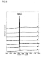
- Figure 5 shows a Raman spectrum chart, as a result of the evaluation by Raman spectroscopy and X-ray diffraction, wherein the measurement and the evaluation were made on the diamond grown as particles having a particle number density of 10 8 /cm 2 and a variation of ⁇ 20 % in the case where the electrode layout was such that the anode diameter was 20 mm and the separation between the anode and the substrate was 8 mm.
- a YAG laser of 532 nm in wavelength was used as the incident light.
- a relatively sharp peak was observed at 1332 cm -1 . From the fact that a sharp peak was observed only at 1332 cm -1 in a measurement for a high pressure high temperature synthesized Ib type diamond, the peak at 1332 cm -1 was found to be ascribable to diamond.
- the bias enhanced nucleation for an Ir base substrate of 1 inch (2.5 cm) or more in diameter is investigated.
- the increase of the current density increases the heat amount generated in the substrate, and hence the substrate temperature at the time of the bias enhanced nucleation is required to be regulated.
- the discharge current is increased, the generated heat amount is proportional to the discharge current, the heat capacity of the substrate holder is proportional to the volume thereof, and hence the ratio between the discharge current and the volume of the substrate holder maintained so as to be constant is probably applicable to the large area formation.
- an optimization of the electrode layout conditions is significant.
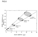
- the appropriate anode diameter is anticipated to be approximately 60 to 70 % of the diameter of the Ir base substrate.
- the ratio between the anode diameter and the separation made to be constant is probably applicable to the large area formation, and hence, for example, a prediction up to the diameter of 12 inches (30 cm) is possible as shown in Figure 6 .
- rough estimations for the respective conditions in relation to the size of the substrate are shown in Table 5. With increasing substrate size, the estimation error is anticipated to increase; however, the cases where the diameter of the Ir base substrate is 12 inches (30 cm) or less can be easily estimated.
- the epitaxial Ir thin film is formed on a single crystal magnesium oxide (MgO) as the substrate; however, the present invention is not limited to these Examples in such a way that, for example, by using a single crystal sapphire ( ⁇ -Al 2 O 3 ) as the substrate, and by setting the plane direction thereof to be ⁇ 0001 ⁇ , an epitaxial Ir thin film can be formed in the same manner as in above-described Examples.
- the method for forming the epitaxial Ir thin film the sputtering method is described above, the vacuum deposition method can also be used. Within the scope not deviating from the spirit of the present invention, various other design modifications may be acceptable.
Landscapes
- Chemical & Material Sciences (AREA)
- Engineering & Computer Science (AREA)
- Materials Engineering (AREA)
- Metallurgy (AREA)
- Organic Chemistry (AREA)
- Crystallography & Structural Chemistry (AREA)
- Analytical Chemistry (AREA)
- Plasma & Fusion (AREA)
- Physics & Mathematics (AREA)
- Chemical Kinetics & Catalysis (AREA)
- General Chemical & Material Sciences (AREA)
- Inorganic Chemistry (AREA)
- Mechanical Engineering (AREA)
- Crystals, And After-Treatments Of Crystals (AREA)
- Chemical Vapour Deposition (AREA)
- Physical Vapour Deposition (AREA)
Applications Claiming Priority (2)
| Application Number | Priority Date | Filing Date | Title |
|---|---|---|---|
| JP2006097697A JP5066651B2 (ja) | 2006-03-31 | 2006-03-31 | エピタキシャルダイヤモンド膜下地基板の製造方法およびこの下地基板を使用するエピタキシャルダイヤモンド膜の製造方法 |
| PCT/JP2007/051915 WO2007116600A1 (fr) | 2006-03-31 | 2007-02-05 | Substrat de base pour une pellicule de diamant épitaxique, procédé de fabrication du substrat de base pour pellicule de diamant épitaxique, pellicule de diamant épitaxique fabriquée par le substrat de base pour pellicule de diamant épitaxique et procédé de fabri |
Publications (3)
| Publication Number | Publication Date |
|---|---|
| EP2009135A1 true EP2009135A1 (fr) | 2008-12-31 |
| EP2009135A4 EP2009135A4 (fr) | 2010-12-29 |
| EP2009135B1 EP2009135B1 (fr) | 2016-05-18 |
Family
ID=38580903
Family Applications (1)
| Application Number | Title | Priority Date | Filing Date |
|---|---|---|---|
| EP07708033.1A Active EP2009135B1 (fr) | 2006-03-31 | 2007-02-05 | Substrat de base pour une pellicule de diamant épitaxique, procédé de fabrication du substrat de base pour pellicule de diamant épitaxique, pellicule de diamant épitaxique fabriquée par le substrat de base pour pellicule de diamant épitaxique et procédé de fabrication de pellicule de diamant épitaxique |
Country Status (4)
| Country | Link |
|---|---|
| US (1) | US9353458B2 (fr) |
| EP (1) | EP2009135B1 (fr) |
| JP (1) | JP5066651B2 (fr) |
| WO (1) | WO2007116600A1 (fr) |
Cited By (3)
| Publication number | Priority date | Publication date | Assignee | Title |
|---|---|---|---|---|
| US20100178234A1 (en) * | 2009-01-09 | 2010-07-15 | Shin-Etsu Chemical Co., Ltd. | Multilayer substrate and method for producing the same, diamond film and method for producing the same |
| CN101892521A (zh) * | 2009-05-20 | 2010-11-24 | 信越化学工业株式会社 | 单晶金刚石层生长用基板以及单晶金刚石基板的制造方法 |
| WO2019051299A1 (fr) * | 2017-09-08 | 2019-03-14 | J2 Materials, Llc | Diamants et procédés hétéro-épitaxiaux de formation de diamants |
Families Citing this family (17)
| Publication number | Priority date | Publication date | Assignee | Title |
|---|---|---|---|---|
| JP2010095408A (ja) * | 2008-10-17 | 2010-04-30 | Agd Material Co Ltd | エピタキシャルダイヤモンド膜および自立したエピタキシャルダイヤモンド基板の製造方法 |
| JP4982506B2 (ja) * | 2009-01-09 | 2012-07-25 | 信越化学工業株式会社 | 単結晶ダイヤモンドの製造方法 |
| US8852519B2 (en) * | 2009-07-09 | 2014-10-07 | Toyota Jidosha Kabushiki Kaisha | Exhaust gas purifying catalyst and production process thereof |
| JP5377212B2 (ja) | 2009-10-13 | 2013-12-25 | 信越化学工業株式会社 | 単結晶ダイヤモンド基板の製造方法 |
| JP5468528B2 (ja) | 2010-06-28 | 2014-04-09 | 信越化学工業株式会社 | 単結晶ダイヤモンド成長用基材及びその製造方法並びに単結晶ダイヤモンド基板の製造方法 |
| JP5929520B2 (ja) * | 2012-05-30 | 2016-06-08 | 住友電気工業株式会社 | ダイヤモンド系膜の製造方法およびそれに用いられる複合基板 |
| TWI481752B (zh) * | 2012-11-20 | 2015-04-21 | Univ Nat Chiao Tung | 鑽石磊晶成長方法 |
| EP3054036B1 (fr) | 2013-09-30 | 2021-03-03 | Adamant Namiki Precision Jewel Co., Ltd. | Procédé de fabrication d'un substrat en diamant |
| KR102106425B1 (ko) | 2014-02-05 | 2020-05-04 | 아다만도 나미키 세이미츠 호오세키 가부시키가이샤 | 다이아몬드 기판 및 다이아몬드 기판의 제조 방법 |
| CN108707965A (zh) * | 2018-06-15 | 2018-10-26 | 西安碳星半导体科技有限公司 | 一种cvd单晶金刚石异质外延衬底的结构及制备方法 |
| CN111206280B (zh) * | 2020-01-07 | 2021-02-12 | 北京科技大学 | 一种高质量大尺寸单晶金刚石外延生长的方法 |
| CN111933514B (zh) * | 2020-08-12 | 2023-02-24 | 哈尔滨工业大学 | 电子束蒸镀工艺制备外延单晶金刚石用Ir(111)复合衬底的方法 |
| JP6998634B1 (ja) | 2020-10-22 | 2022-01-18 | 国立大学法人長岡技術科学大学 | ダイヤモンド形成用構造体、およびダイヤモンド形成用構造体の製造方法 |
| JP7253208B2 (ja) | 2021-07-09 | 2023-04-06 | 株式会社ディスコ | ダイヤモンド成膜方法及びダイヤモンド成膜装置 |
| CN114318287B (zh) * | 2021-12-23 | 2023-11-03 | 深圳技术大学 | 金刚石自支撑膜的制备方法和金刚石自支撑膜 |
| CN115637431B (zh) * | 2022-10-28 | 2024-11-19 | 武汉莱格晶钻科技有限公司 | 一种硅片衬底表面预处理方法及其应用 |
| CN116988150A (zh) * | 2023-02-28 | 2023-11-03 | 中国电子科技集团公司第四十六研究所 | 一种基于结构复合衬底异质外延生长金刚石的方法 |
Family Cites Families (16)
| Publication number | Priority date | Publication date | Assignee | Title |
|---|---|---|---|---|
| US5647964A (en) * | 1995-06-02 | 1997-07-15 | Korea Institute Of Science And Technology | Diamond film synthesizing apparatus and method thereof using direct current glow discharge plasma enhanced chemical vapor deposition |
| JP4374823B2 (ja) * | 2002-03-22 | 2009-12-02 | 住友電気工業株式会社 | ダイヤモンド単結晶の製造方法およびダイヤモンド単結晶基板の製造方法 |
| US7060130B2 (en) * | 2002-08-27 | 2006-06-13 | Board Of Trustees Of Michigan State University | Heteroepitaxial diamond and diamond nuclei precursors |
| JP4528654B2 (ja) * | 2005-03-14 | 2010-08-18 | 信越化学工業株式会社 | 積層基板、積層基板の製造方法及びデバイス |
| US7550385B2 (en) * | 2005-09-30 | 2009-06-23 | Intel Corporation | Amine-free deposition of metal-nitride films |
| WO2007092893A2 (fr) * | 2006-02-07 | 2007-08-16 | Target Technology Company, Llc | Materiaux et procedes de fabrication de diamants monocristallins de grande dimension |
| US20090004093A1 (en) * | 2006-02-07 | 2009-01-01 | Nee Han H | Materials and methods for the manufacture of large crystal diamonds |
| JP5053553B2 (ja) * | 2006-03-08 | 2012-10-17 | 信越化学工業株式会社 | 単結晶ダイヤモンド成長用基材の製造方法 |
| JP2010159185A (ja) * | 2009-01-09 | 2010-07-22 | Shin-Etsu Chemical Co Ltd | 積層基板とその製造方法及びダイヤモンド膜とその製造方法 |
| JP4982506B2 (ja) * | 2009-01-09 | 2012-07-25 | 信越化学工業株式会社 | 単結晶ダイヤモンドの製造方法 |
| JP5507888B2 (ja) * | 2009-05-20 | 2014-05-28 | 信越化学工業株式会社 | 単結晶ダイヤモンド層成長用基板及び単結晶ダイヤモンド基板の製造方法 |
| JP2011079683A (ja) * | 2009-10-02 | 2011-04-21 | Shin-Etsu Chemical Co Ltd | 単結晶ダイヤモンド成長用基材及び単結晶ダイヤモンド基板の製造方法 |
| JP5377212B2 (ja) * | 2009-10-13 | 2013-12-25 | 信越化学工業株式会社 | 単結晶ダイヤモンド基板の製造方法 |
| JP5468528B2 (ja) * | 2010-06-28 | 2014-04-09 | 信越化学工業株式会社 | 単結晶ダイヤモンド成長用基材及びその製造方法並びに単結晶ダイヤモンド基板の製造方法 |
| JP5842761B2 (ja) * | 2012-08-07 | 2016-01-13 | 信越化学工業株式会社 | ダイヤモンドの製造方法及び直流プラズマcvd装置 |
| JP6112485B2 (ja) * | 2013-09-19 | 2017-04-12 | 国立研究開発法人産業技術総合研究所 | 単結晶ダイヤモンドの製造方法 |
-
2006
- 2006-03-31 JP JP2006097697A patent/JP5066651B2/ja not_active Expired - Fee Related
-
2007
- 2007-02-05 EP EP07708033.1A patent/EP2009135B1/fr active Active
- 2007-02-05 US US12/225,570 patent/US9353458B2/en active Active
- 2007-02-05 WO PCT/JP2007/051915 patent/WO2007116600A1/fr not_active Ceased
Cited By (7)
| Publication number | Priority date | Publication date | Assignee | Title |
|---|---|---|---|---|
| US20100178234A1 (en) * | 2009-01-09 | 2010-07-15 | Shin-Etsu Chemical Co., Ltd. | Multilayer substrate and method for producing the same, diamond film and method for producing the same |
| CN101892521A (zh) * | 2009-05-20 | 2010-11-24 | 信越化学工业株式会社 | 单晶金刚石层生长用基板以及单晶金刚石基板的制造方法 |
| WO2019051299A1 (fr) * | 2017-09-08 | 2019-03-14 | J2 Materials, Llc | Diamants et procédés hétéro-épitaxiaux de formation de diamants |
| EP3679000A4 (fr) * | 2017-09-08 | 2021-06-16 | J2 Materials, LLC | Diamants et procédés hétéro-épitaxiaux de formation de diamants |
| US11198950B2 (en) | 2017-09-08 | 2021-12-14 | M7D Corporation | Diamonds and hetero-epitaxial methods of forming diamonds |
| US11905619B2 (en) | 2017-09-08 | 2024-02-20 | M7D Corporation | Diamonds and hetero-epitaxial methods of forming diamonds |
| US12371815B2 (en) | 2017-09-08 | 2025-07-29 | Advanced Diamond Holdings, Llc | Diamonds and hetero-epitaxial method of forming diamonds |
Also Published As
| Publication number | Publication date |
|---|---|
| EP2009135A4 (fr) | 2010-12-29 |
| JP5066651B2 (ja) | 2012-11-07 |
| EP2009135B1 (fr) | 2016-05-18 |
| WO2007116600A1 (fr) | 2007-10-18 |
| JP2007270272A (ja) | 2007-10-18 |
| US20090176114A1 (en) | 2009-07-09 |
| US9353458B2 (en) | 2016-05-31 |
Similar Documents
| Publication | Publication Date | Title |
|---|---|---|
| EP2009135B1 (fr) | Substrat de base pour une pellicule de diamant épitaxique, procédé de fabrication du substrat de base pour pellicule de diamant épitaxique, pellicule de diamant épitaxique fabriquée par le substrat de base pour pellicule de diamant épitaxique et procédé de fabrication de pellicule de diamant épitaxique | |
| CN102041551B (zh) | 单晶金刚石生长用基材及单晶金刚石基板的制造方法 | |
| EP2851457B1 (fr) | Procédé pour la fabrictaion d'un monocristal de diamant | |
| JPH05506064A (ja) | 電子用途用ダイヤモンド載置基板 | |
| JP4528654B2 (ja) | 積層基板、積層基板の製造方法及びデバイス | |
| GB2219578A (en) | Manufacturing single-crystal diamond particles | |
| CN110228806A (zh) | 利用等离子增强化学气相沉积法制备石墨烯薄膜的方法 | |
| JP2010095408A (ja) | エピタキシャルダイヤモンド膜および自立したエピタキシャルダイヤモンド基板の製造方法 | |
| US5993919A (en) | Method of synthesizing diamond | |
| Kondo et al. | Synthesis of diamond-like carbon films by nanopulse plasma chemical vapor deposition in open air | |
| EP4357492A1 (fr) | Substrat de diamant et son procédé de fabrication | |
| Ali et al. | Combined substrate polishing and biasing during hot-filament chemical vapor deposition of diamond on copper | |
| US10337102B2 (en) | Process for producing a graphene film | |
| JPH04160074A (ja) | ダイヤモンド多孔質体及びその製造方法 | |
| US20240175136A1 (en) | Manufacturing method for graphene film | |
| JP5042134B2 (ja) | ダイヤモンド薄膜 | |
| KR20170083782A (ko) | 보론 도핑 다이아몬드 박막 형성방법 및 이에 의해 제조된 보론 도핑 다이아몬드 피증착 부재 | |
| JPS60186500A (ja) | 気相からのダイヤモンド合成法 | |
| JP2025002656A (ja) | ダイヤモンド薄膜及びダイヤモンド薄膜の製造方法 | |
| TW202421578A (zh) | 奈米石墨烯壁、其製造方法、電極以及超級電容器 | |
| JPH04240190A (ja) | CVD法によるSi基板へのダイヤモンド膜形成方法 | |
| Jin | Research and Development of a New Field Enhanced Low Temperature Thermionic Cathode that Enables Fluorescent Dimming and Loan Shedding without Auxiliary Cathode Heating | |
| JPH04139090A (ja) | ダイヤモンドの製造方法 | |
| JPS61236113A (ja) | ダイヤモンド薄膜及びp型ダイヤモンド半導体の製造方法 | |
| JP2617374C (fr) |
Legal Events
| Date | Code | Title | Description |
|---|---|---|---|
| PUAI | Public reference made under article 153(3) epc to a published international application that has entered the european phase |
Free format text: ORIGINAL CODE: 0009012 |
|
| 17P | Request for examination filed |
Effective date: 20081022 |
|
| AK | Designated contracting states |
Kind code of ref document: A1 Designated state(s): AT BE BG CH CY CZ DE DK EE ES FI FR GB GR HU IE IS IT LI LT LU LV MC NL PL PT RO SE SI SK TR |
|
| AX | Request for extension of the european patent |
Extension state: AL BA HR MK RS |
|
| RIN1 | Information on inventor provided before grant (corrected) |
Inventor name: SAWABE, ATSUHITO Inventor name: MAEDA, SHINTARO |
|
| RIN1 | Information on inventor provided before grant (corrected) |
Inventor name: NOGUCHI, HITOSHI Inventor name: SAWABE, ATSUHITO Inventor name: MAEDA, SHINTARO |
|
| A4 | Supplementary search report drawn up and despatched |
Effective date: 20101130 |
|
| DAX | Request for extension of the european patent (deleted) | ||
| 17Q | First examination report despatched |
Effective date: 20130218 |
|
| REG | Reference to a national code |
Ref country code: DE Ref legal event code: R079 Ref document number: 602007046354 Country of ref document: DE Free format text: PREVIOUS MAIN CLASS: C23C0016020000 Ipc: C30B0025100000 |
|
| RIC1 | Information provided on ipc code assigned before grant |
Ipc: C30B 23/02 20060101ALI20151016BHEP Ipc: C30B 25/10 20060101AFI20151016BHEP Ipc: C23C 16/27 20060101ALI20151016BHEP Ipc: C23C 16/02 20060101ALI20151016BHEP Ipc: C30B 29/04 20060101ALI20151016BHEP Ipc: H01J 37/34 20060101ALI20151016BHEP Ipc: C30B 25/18 20060101ALI20151016BHEP Ipc: C30B 29/02 20060101ALI20151016BHEP Ipc: H01J 37/32 20060101ALI20151016BHEP Ipc: H01L 21/02 20060101ALI20151016BHEP |
|
| GRAP | Despatch of communication of intention to grant a patent |
Free format text: ORIGINAL CODE: EPIDOSNIGR1 |
|
| INTG | Intention to grant announced |
Effective date: 20151214 |
|
| RIN1 | Information on inventor provided before grant (corrected) |
Inventor name: SAWABE, ATSUHITO Inventor name: NOGUCHI, HITOSHI Inventor name: MAEDA, SHINTARO |
|
| GRAS | Grant fee paid |
Free format text: ORIGINAL CODE: EPIDOSNIGR3 |
|
| GRAA | (expected) grant |
Free format text: ORIGINAL CODE: 0009210 |
|
| RAP1 | Party data changed (applicant data changed or rights of an application transferred) |
Owner name: IMAI, YOSHIO Owner name: SAWABE, ATSUHITO |
|
| RIN1 | Information on inventor provided before grant (corrected) |
Inventor name: SAWABE, ATSUHITO Inventor name: MAEDA, SHINTARO Inventor name: NOGUCHI, HITOSHI |
|
| AK | Designated contracting states |
Kind code of ref document: B1 Designated state(s): AT BE BG CH CY CZ DE DK EE ES FI FR GB GR HU IE IS IT LI LT LU LV MC NL PL PT RO SE SI SK TR |
|
| REG | Reference to a national code |
Ref country code: GB Ref legal event code: FG4D |
|
| REG | Reference to a national code |
Ref country code: CH Ref legal event code: EP |
|
| REG | Reference to a national code |
Ref country code: IE Ref legal event code: FG4D Ref country code: AT Ref legal event code: REF Ref document number: 800549 Country of ref document: AT Kind code of ref document: T Effective date: 20160615 |
|
| REG | Reference to a national code |
Ref country code: DE Ref legal event code: R096 Ref document number: 602007046354 Country of ref document: DE |
|
| REG | Reference to a national code |
Ref country code: NL Ref legal event code: MP Effective date: 20160518 |
|
| REG | Reference to a national code |
Ref country code: LT Ref legal event code: MG4D |
|
| PG25 | Lapsed in a contracting state [announced via postgrant information from national office to epo] |
Ref country code: LT Free format text: LAPSE BECAUSE OF FAILURE TO SUBMIT A TRANSLATION OF THE DESCRIPTION OR TO PAY THE FEE WITHIN THE PRESCRIBED TIME-LIMIT Effective date: 20160518 Ref country code: NL Free format text: LAPSE BECAUSE OF FAILURE TO SUBMIT A TRANSLATION OF THE DESCRIPTION OR TO PAY THE FEE WITHIN THE PRESCRIBED TIME-LIMIT Effective date: 20160518 Ref country code: FI Free format text: LAPSE BECAUSE OF FAILURE TO SUBMIT A TRANSLATION OF THE DESCRIPTION OR TO PAY THE FEE WITHIN THE PRESCRIBED TIME-LIMIT Effective date: 20160518 |
|
| REG | Reference to a national code |
Ref country code: AT Ref legal event code: MK05 Ref document number: 800549 Country of ref document: AT Kind code of ref document: T Effective date: 20160518 |
|
| PG25 | Lapsed in a contracting state [announced via postgrant information from national office to epo] |
Ref country code: GR Free format text: LAPSE BECAUSE OF FAILURE TO SUBMIT A TRANSLATION OF THE DESCRIPTION OR TO PAY THE FEE WITHIN THE PRESCRIBED TIME-LIMIT Effective date: 20160819 Ref country code: PT Free format text: LAPSE BECAUSE OF FAILURE TO SUBMIT A TRANSLATION OF THE DESCRIPTION OR TO PAY THE FEE WITHIN THE PRESCRIBED TIME-LIMIT Effective date: 20160919 Ref country code: SE Free format text: LAPSE BECAUSE OF FAILURE TO SUBMIT A TRANSLATION OF THE DESCRIPTION OR TO PAY THE FEE WITHIN THE PRESCRIBED TIME-LIMIT Effective date: 20160518 Ref country code: ES Free format text: LAPSE BECAUSE OF FAILURE TO SUBMIT A TRANSLATION OF THE DESCRIPTION OR TO PAY THE FEE WITHIN THE PRESCRIBED TIME-LIMIT Effective date: 20160518 Ref country code: LV Free format text: LAPSE BECAUSE OF FAILURE TO SUBMIT A TRANSLATION OF THE DESCRIPTION OR TO PAY THE FEE WITHIN THE PRESCRIBED TIME-LIMIT Effective date: 20160518 |
|
| PG25 | Lapsed in a contracting state [announced via postgrant information from national office to epo] |
Ref country code: IT Free format text: LAPSE BECAUSE OF FAILURE TO SUBMIT A TRANSLATION OF THE DESCRIPTION OR TO PAY THE FEE WITHIN THE PRESCRIBED TIME-LIMIT Effective date: 20160518 |
|
| PG25 | Lapsed in a contracting state [announced via postgrant information from national office to epo] |
Ref country code: DK Free format text: LAPSE BECAUSE OF FAILURE TO SUBMIT A TRANSLATION OF THE DESCRIPTION OR TO PAY THE FEE WITHIN THE PRESCRIBED TIME-LIMIT Effective date: 20160518 Ref country code: EE Free format text: LAPSE BECAUSE OF FAILURE TO SUBMIT A TRANSLATION OF THE DESCRIPTION OR TO PAY THE FEE WITHIN THE PRESCRIBED TIME-LIMIT Effective date: 20160518 Ref country code: SK Free format text: LAPSE BECAUSE OF FAILURE TO SUBMIT A TRANSLATION OF THE DESCRIPTION OR TO PAY THE FEE WITHIN THE PRESCRIBED TIME-LIMIT Effective date: 20160518 Ref country code: CZ Free format text: LAPSE BECAUSE OF FAILURE TO SUBMIT A TRANSLATION OF THE DESCRIPTION OR TO PAY THE FEE WITHIN THE PRESCRIBED TIME-LIMIT Effective date: 20160518 Ref country code: RO Free format text: LAPSE BECAUSE OF FAILURE TO SUBMIT A TRANSLATION OF THE DESCRIPTION OR TO PAY THE FEE WITHIN THE PRESCRIBED TIME-LIMIT Effective date: 20160518 |
|
| REG | Reference to a national code |
Ref country code: DE Ref legal event code: R097 Ref document number: 602007046354 Country of ref document: DE |
|
| REG | Reference to a national code |
Ref country code: FR Ref legal event code: PLFP Year of fee payment: 11 |
|
| PG25 | Lapsed in a contracting state [announced via postgrant information from national office to epo] |
Ref country code: PL Free format text: LAPSE BECAUSE OF FAILURE TO SUBMIT A TRANSLATION OF THE DESCRIPTION OR TO PAY THE FEE WITHIN THE PRESCRIBED TIME-LIMIT Effective date: 20160518 Ref country code: AT Free format text: LAPSE BECAUSE OF FAILURE TO SUBMIT A TRANSLATION OF THE DESCRIPTION OR TO PAY THE FEE WITHIN THE PRESCRIBED TIME-LIMIT Effective date: 20160518 |
|
| PLBE | No opposition filed within time limit |
Free format text: ORIGINAL CODE: 0009261 |
|
| STAA | Information on the status of an ep patent application or granted ep patent |
Free format text: STATUS: NO OPPOSITION FILED WITHIN TIME LIMIT |
|
| 26N | No opposition filed |
Effective date: 20170221 |
|
| PG25 | Lapsed in a contracting state [announced via postgrant information from national office to epo] |
Ref country code: SI Free format text: LAPSE BECAUSE OF FAILURE TO SUBMIT A TRANSLATION OF THE DESCRIPTION OR TO PAY THE FEE WITHIN THE PRESCRIBED TIME-LIMIT Effective date: 20160518 |
|
| PG25 | Lapsed in a contracting state [announced via postgrant information from national office to epo] |
Ref country code: MC Free format text: LAPSE BECAUSE OF FAILURE TO SUBMIT A TRANSLATION OF THE DESCRIPTION OR TO PAY THE FEE WITHIN THE PRESCRIBED TIME-LIMIT Effective date: 20160518 |
|
| REG | Reference to a national code |
Ref country code: IE Ref legal event code: MM4A |
|
| PG25 | Lapsed in a contracting state [announced via postgrant information from national office to epo] |
Ref country code: LU Free format text: LAPSE BECAUSE OF NON-PAYMENT OF DUE FEES Effective date: 20170205 |
|
| REG | Reference to a national code |
Ref country code: FR Ref legal event code: PLFP Year of fee payment: 12 |
|
| PG25 | Lapsed in a contracting state [announced via postgrant information from national office to epo] |
Ref country code: IE Free format text: LAPSE BECAUSE OF NON-PAYMENT OF DUE FEES Effective date: 20170205 |
|
| PG25 | Lapsed in a contracting state [announced via postgrant information from national office to epo] |
Ref country code: HU Free format text: LAPSE BECAUSE OF FAILURE TO SUBMIT A TRANSLATION OF THE DESCRIPTION OR TO PAY THE FEE WITHIN THE PRESCRIBED TIME-LIMIT; INVALID AB INITIO Effective date: 20070205 |
|
| PG25 | Lapsed in a contracting state [announced via postgrant information from national office to epo] |
Ref country code: BG Free format text: LAPSE BECAUSE OF FAILURE TO SUBMIT A TRANSLATION OF THE DESCRIPTION OR TO PAY THE FEE WITHIN THE PRESCRIBED TIME-LIMIT Effective date: 20160518 |
|
| PG25 | Lapsed in a contracting state [announced via postgrant information from national office to epo] |
Ref country code: CY Free format text: LAPSE BECAUSE OF NON-PAYMENT OF DUE FEES Effective date: 20160518 |
|
| PG25 | Lapsed in a contracting state [announced via postgrant information from national office to epo] |
Ref country code: TR Free format text: LAPSE BECAUSE OF FAILURE TO SUBMIT A TRANSLATION OF THE DESCRIPTION OR TO PAY THE FEE WITHIN THE PRESCRIBED TIME-LIMIT Effective date: 20160518 |
|
| PG25 | Lapsed in a contracting state [announced via postgrant information from national office to epo] |
Ref country code: IS Free format text: LAPSE BECAUSE OF FAILURE TO SUBMIT A TRANSLATION OF THE DESCRIPTION OR TO PAY THE FEE WITHIN THE PRESCRIBED TIME-LIMIT Effective date: 20160918 |
|
| PGFP | Annual fee paid to national office [announced via postgrant information from national office to epo] |
Ref country code: DE Payment date: 20231228 Year of fee payment: 18 Ref country code: GB Payment date: 20240109 Year of fee payment: 18 Ref country code: CH Payment date: 20240301 Year of fee payment: 18 |
|
| PGFP | Annual fee paid to national office [announced via postgrant information from national office to epo] |
Ref country code: FR Payment date: 20240103 Year of fee payment: 18 Ref country code: BE Payment date: 20240105 Year of fee payment: 18 |
|
| REG | Reference to a national code |
Ref country code: DE Ref legal event code: R119 Ref document number: 602007046354 Country of ref document: DE |
|
| REG | Reference to a national code |
Ref country code: CH Ref legal event code: PL |
|
| PG25 | Lapsed in a contracting state [announced via postgrant information from national office to epo] |
Ref country code: CH Free format text: LAPSE BECAUSE OF NON-PAYMENT OF DUE FEES Effective date: 20250228 |
|
| GBPC | Gb: european patent ceased through non-payment of renewal fee |
Effective date: 20250205 |
|
| REG | Reference to a national code |
Ref country code: BE Ref legal event code: MM Effective date: 20250228 |
|
| PG25 | Lapsed in a contracting state [announced via postgrant information from national office to epo] |
Ref country code: DE Free format text: LAPSE BECAUSE OF NON-PAYMENT OF DUE FEES Effective date: 20250902 |
|
| PG25 | Lapsed in a contracting state [announced via postgrant information from national office to epo] |
Ref country code: GB Free format text: LAPSE BECAUSE OF NON-PAYMENT OF DUE FEES Effective date: 20250205 |
|
| PG25 | Lapsed in a contracting state [announced via postgrant information from national office to epo] |
Ref country code: FR Free format text: LAPSE BECAUSE OF NON-PAYMENT OF DUE FEES Effective date: 20250228 |
|
| PG25 | Lapsed in a contracting state [announced via postgrant information from national office to epo] |
Ref country code: BE Free format text: LAPSE BECAUSE OF NON-PAYMENT OF DUE FEES Effective date: 20250228 |