EP2009461A1 - Radar à impulsions brèves et procédé de contrôle dudit radar - Google Patents
Radar à impulsions brèves et procédé de contrôle dudit radar Download PDFInfo
- Publication number
- EP2009461A1 EP2009461A1 EP07715168A EP07715168A EP2009461A1 EP 2009461 A1 EP2009461 A1 EP 2009461A1 EP 07715168 A EP07715168 A EP 07715168A EP 07715168 A EP07715168 A EP 07715168A EP 2009461 A1 EP2009461 A1 EP 2009461A1
- Authority
- EP
- European Patent Office
- Prior art keywords
- signal
- receiving
- short
- pulse
- range radar
- Prior art date
- Legal status (The legal status is an assumption and is not a legal conclusion. Google has not performed a legal analysis and makes no representation as to the accuracy of the status listed.)
- Withdrawn
Links
- 238000000034 method Methods 0.000 title claims description 94
- 238000001228 spectrum Methods 0.000 claims abstract description 41
- 238000001514 detection method Methods 0.000 claims description 63
- 230000005540 biological transmission Effects 0.000 claims description 48
- 238000012545 processing Methods 0.000 claims description 29
- 230000010354 integration Effects 0.000 claims description 20
- 238000002955 isolation Methods 0.000 claims description 16
- 230000010355 oscillation Effects 0.000 claims description 12
- 239000000284 extract Substances 0.000 claims description 9
- 230000001360 synchronised effect Effects 0.000 claims description 4
- 230000001934 delay Effects 0.000 claims description 2
- 230000002452 interceptive effect Effects 0.000 abstract 1
- 238000010586 diagram Methods 0.000 description 27
- 239000000758 substrate Substances 0.000 description 12
- 239000002184 metal Substances 0.000 description 8
- 239000004020 conductor Substances 0.000 description 7
- 230000010287 polarization Effects 0.000 description 5
- 230000033228 biological regulation Effects 0.000 description 4
- 238000004891 communication Methods 0.000 description 4
- 230000003111 delayed effect Effects 0.000 description 4
- 230000000694 effects Effects 0.000 description 2
- 238000007747 plating Methods 0.000 description 2
- 230000006641 stabilisation Effects 0.000 description 2
- 238000011105 stabilization Methods 0.000 description 2
- 230000002238 attenuated effect Effects 0.000 description 1
- 239000003990 capacitor Substances 0.000 description 1
- 238000003379 elimination reaction Methods 0.000 description 1
- 230000005284 excitation Effects 0.000 description 1
- 238000000605 extraction Methods 0.000 description 1
- 238000003780 insertion Methods 0.000 description 1
- 230000037431 insertion Effects 0.000 description 1
- 230000010363 phase shift Effects 0.000 description 1
- 238000002310 reflectometry Methods 0.000 description 1
- 230000002441 reversible effect Effects 0.000 description 1
- 238000011896 sensitive detection Methods 0.000 description 1
- 230000035945 sensitivity Effects 0.000 description 1
- 230000001629 suppression Effects 0.000 description 1
- 238000012360 testing method Methods 0.000 description 1
Images







Classifications
-
- G—PHYSICS
- G01—MEASURING; TESTING
- G01S—RADIO DIRECTION-FINDING; RADIO NAVIGATION; DETERMINING DISTANCE OR VELOCITY BY USE OF RADIO WAVES; LOCATING OR PRESENCE-DETECTING BY USE OF THE REFLECTION OR RERADIATION OF RADIO WAVES; ANALOGOUS ARRANGEMENTS USING OTHER WAVES
- G01S13/00—Systems using the reflection or reradiation of radio waves, e.g. radar systems; Analogous systems using reflection or reradiation of waves whose nature or wavelength is irrelevant or unspecified
- G01S13/02—Systems using reflection of radio waves, e.g. primary radar systems; Analogous systems
- G01S13/06—Systems determining position data of a target
- G01S13/08—Systems for measuring distance only
- G01S13/10—Systems for measuring distance only using transmission of interrupted, pulse modulated waves
- G01S13/106—Systems for measuring distance only using transmission of interrupted, pulse modulated waves using transmission of pulses having some particular characteristics
-
- G—PHYSICS
- G01—MEASURING; TESTING
- G01S—RADIO DIRECTION-FINDING; RADIO NAVIGATION; DETERMINING DISTANCE OR VELOCITY BY USE OF RADIO WAVES; LOCATING OR PRESENCE-DETECTING BY USE OF THE REFLECTION OR RERADIATION OF RADIO WAVES; ANALOGOUS ARRANGEMENTS USING OTHER WAVES
- G01S7/00—Details of systems according to groups G01S13/00, G01S15/00, G01S17/00
- G01S7/02—Details of systems according to groups G01S13/00, G01S15/00, G01S17/00 of systems according to group G01S13/00
- G01S7/28—Details of pulse systems
- G01S7/282—Transmitters
-
- H—ELECTRICITY
- H01—ELECTRIC ELEMENTS
- H01Q—ANTENNAS, i.e. RADIO AERIALS
- H01Q21/00—Antenna arrays or systems
- H01Q21/06—Arrays of individually energised antenna units similarly polarised and spaced apart
- H01Q21/061—Two dimensional planar arrays
-
- H—ELECTRICITY
- H01—ELECTRIC ELEMENTS
- H01Q—ANTENNAS, i.e. RADIO AERIALS
- H01Q9/00—Electrically-short antennas having dimensions not more than twice the operating wavelength and consisting of conductive active radiating elements
- H01Q9/04—Resonant antennas
- H01Q9/16—Resonant antennas with feed intermediate between the extremities of the antenna, e.g. centre-fed dipole
- H01Q9/26—Resonant antennas with feed intermediate between the extremities of the antenna, e.g. centre-fed dipole with folded element or elements, the folded parts being spaced apart a small fraction of operating wavelength
- H01Q9/27—Spiral antennas
-
- H—ELECTRICITY
- H04—ELECTRIC COMMUNICATION TECHNIQUE
- H04B—TRANSMISSION
- H04B1/00—Details of transmission systems, not covered by a single one of groups H04B3/00 - H04B13/00; Details of transmission systems not characterised by the medium used for transmission
- H04B1/69—Spread spectrum techniques
- H04B1/7163—Spread spectrum techniques using impulse radio
- H04B1/717—Pulse-related aspects
- H04B1/7174—Pulse generation
-
- G—PHYSICS
- G01—MEASURING; TESTING
- G01S—RADIO DIRECTION-FINDING; RADIO NAVIGATION; DETERMINING DISTANCE OR VELOCITY BY USE OF RADIO WAVES; LOCATING OR PRESENCE-DETECTING BY USE OF THE REFLECTION OR RERADIATION OF RADIO WAVES; ANALOGOUS ARRANGEMENTS USING OTHER WAVES
- G01S13/00—Systems using the reflection or reradiation of radio waves, e.g. radar systems; Analogous systems using reflection or reradiation of waves whose nature or wavelength is irrelevant or unspecified
- G01S13/02—Systems using reflection of radio waves, e.g. primary radar systems; Analogous systems
- G01S13/0209—Systems with very large relative bandwidth, i.e. larger than 10 %, e.g. baseband, pulse, carrier-free, ultrawideband
Definitions
- the present invention relates to a short-range radar and a control method thereof, and particularly to a short-range radar using UWB (Ultra Wideband) of 22 to 29 GHz employing a technique exactly complying with the stipulation of the International Radio Communication Regulations (RR) and a control method thereof.
- UWB Ultra Wideband
- the short pulse wave is emitted from the antenna of a transmitting unit into the space, and a receiving unit receives the wave reflected from an object existing in the space thereby to analyze the object.
- FIG. 24 is a block diagram showing the general configuration of the transmitting unit of the conventional short-range radar of this type.
- a carrier signal S of a predetermined UWB frequency output continuously from a carrier signal generator 1 is input to a switch circuit 2.
- the switch circuit 2 is intermittently turned on/off by a pulse signal Pa output from a pulse generator 3 in a predetermined period thereby to generate a short pulse wave (burst carrier) Pb.
- This short pulse wave (burst carrier) Pb after being amplified by an amplifier 4, is emitted into the space from an antenna 5.
- the turn-off period (for example, 1 ⁇ s) of the switch circuit 2 is normally very long as compared with the turn-on period (for example, 1 ns) thereof. On the average, therefore, the power of the carrier leak is not ignorable.
- the spectrum density Sx of the short pulse wave Pb is such that the leak component S' is projected considerably at the position of the carrier frequency fc.
- This leak component S' limits the real receiving sensitivity of the reflected wave of the short pulse wave Pb output at the regular transmission timing. As a result, the radar search range is narrowed, and it becomes difficult to detect an obstacle of a low reflectivity as an object existing in the space.
- FCC Federal Communication Commission of USA
- the power density of UWB in the range of 22.0 to 23.12 GHz and the range not lower than 29.0 GHz is specified at -61.3 dBm/MHz or less on the one hand, and the power density in the range of 23.12 to 23.6 GHz and the range of 24.0 to 29.0 GHz is specified at -41.3 dBm/MHz or less.
- the emission power density is suppressed to -61.3 dBm/MHz lower by 20 dB than in the past.
- the total energy amount in each predetermined band is restricted to not more than a specified value.
- the output of the short pulse wave Pb for the regular transmission timing is required to be set at a correspondingly low level, resulting in a considerable limitation of the search range of the radar.
- the carrier frequency of the short pulse wave Pb is made to coincide with the UWB frequency band of 24.05 to 24.25 GHz for the Doppler radar (Short Range Device: SRD) where the emission of the power of a higher level than -41.3 dBm/MHz is permitted.
- SRD Short Range Device
- the short pulse wave Pb constituting the pulse modulation signal as a carrier signal turned on/off intermittently by the pulse signal has a spectrum width of several hundred MHz to 2 GHz.
- the carrier frequency is set at the SRD band in the neighborhood of the RR prohibited band as described above, therefore, the considerably high level portion of the spectrum of the short pulse wave Pb is superposed with the RR prohibited band. Actually, therefore, it is very difficult to suppress the emission power density to -61.3 dBm or less specified by the latest spectrum mask.
- the first FCC standard permitting the emission level in the RR prohibited band up to -41.3 dBm/MHz stipulates that in order not to interfere with the EESS described above, the emission strength of the radiowave used for other purposes at the angle of emission direction (direction of elevation) larger than 30° from the normal to the globe surface is required to be lower than the emission strength in the emission range of 0° to 30° by -25 dB or more (in and after January, 2005). This standard has since become increasingly stricter for each several years.
- the side lobe of the vertical surface of the antenna is required to be suppressed so as not to increase the direction of emission of transmitted radiowave.
- the present invention has been achieved in view of the situation described above, and an object thereof is to provide a short-range radar having an inexpensive configuration and a control method thereof in which the interference with the RR prohibited band and the SRD band is prevented while at the same time complying with the stipulated spectrum mask.
- a short-range radar comprising:
- a width Tc of the first pulse (P1), a width Tp of the second pulse (P2) and isolation I of the switch (26) are set to satisfy the following relation: Tc / Tp 2 ⁇ I
- the short-range radar according to the first aspect, wherein an oscillation frequency of the oscillator (25) and the width Tp of the second pulse (P2) are set in such a manner that substantially a whole main lobe of the spectrum of the short pulse wave (Pt) emitted into the space (1) is included in the range of 24.0 to 29.0 GHz.
- the short-range radar in order to achieve the above object, there is provided the short-range radar according to the third aspect, wherein the transmission antenna (22) of the transmitting unit (21) has a structure surrounding an antenna element (123) with a cavity (130), and a resonance frequency of the cavity (130) is set in the band of 23.6 to 24.0 GHz thereby to reduce a gain of the particular band.
- the receiving unit (40) includes:
- the receiving unit (40) includes:
- the receiving unit (40) includes:
- the receiving unit (40) includes:
- the linear multiplier (46) includes:
- the short-range radar according to the first aspect, further comprising an analog/digital converter (60) which converts the output signal (H) from the receiving unit (40) into a digital signal and inputs the digital signal to the signal processing unit (61).
- the short-range radar according to the first aspect, further comprising a control unit (62) which controls at least one of the transmitting unit (21) and the receiving unit (40) in accordance with a predetermined schedule or a processing result from the signal processing unit (61).
- a method of controlling a short-range radar comprising:
- a width Tc of the first pulse (P1), a width Tp of the second pulse (P2) and isolation I of the switch (26) are set to satisfy the following relation: Tc / Tp 2 ⁇ I
- an oscillation frequency of the oscillator (25) and the width Tp of the second pulse (P2) are set in such a manner that substantially a whole main lobe of the spectrum of the short pulse wave (Pt) emitted into the space (1) is included in the range of 24.0 to 29.0 GHz.
- the transmission antenna (22) has a structure surrounding an antenna element (123) with a cavity (130), and a resonance frequency of the cavity (130) is set in the band of 23.6 to 24.0 GHz thereby to reduce a gain of the particular band.
- the method of controlling a short-range radar includes:
- the method of controlling a short-range radar includes:
- the method of controlling a short-range radar includes:
- the method of controlling a short-range radar includes:
- the method of controlling a short-range radar includes:
- the method of controlling a short-range radar according to the twelfth aspect further comprising:
- the method of controlling a short-range radar according to the twelfth aspect further comprising:
- the transmitting unit of the short-range radar according to the invention is adapted to output the short pulse wave by closing the switch for a short time in response to the second pulse in a stable state upon the lapse of a predetermined time after the oscillation is started by the first pulse.
- the leak from the switch with the first pulse not output can be reduced to zero.
- the output period of the first pulse is sufficiently short as compared with the period of the short pulse wave, therefore, the average leak amount can be reduced even by use of an inexpensive switch not very high in isolation.
- the emission power density of the short-range radar as a whole can be suppressed within the specified range of the spectrum mask.
- the average leak amount can be suppressed to not more than the power of the short pulse wave output in synchronism with the second pulse.
- the emission of radiowave to the RR prohibited band and the SRD band can prevented more positively.
- the transmission antenna may be structured to surround the antenna elements with a cavity and have the resonance frequency of the cavity in the range of 23.6 to 24.0 GHz.
- FIG. 1 is a block diagram showing the general configuration of a short-range radar and a control method thereof according to a first embodiment of the invention.
- a short-range radar 20 basically includes: a transmitting unit 21 for emitting a predetermined short pulse wave Pt from a transmission antenna 22 into a space 1; a receiving unit 40 for executing a process of receiving a reflected wave Pr from an object 1a existing in the space 1; and a signal processing unit 61 for executing a process of analyzing the object 1a based on the output signal from the receiving unit 40, wherein the transmitting unit 21 includes: a first pulse generating unit 23 for outputting a first pulse P1 having a width Tc longer than the width of the short pulse wave Pt in a predetermined period Tg; a second pulse generating unit 24 for outputting a second pulse P2 having the width corresponding to the width of the short pulse wave Pt at a timing upon the lapse of a predetermined time Ts from the time point when the first pulse generating unit 23 starts to output the first pulse P1 and during the output period thereof; an oscillator 25 for oscillating and outputting the signal in the frequency band of the short pulse
- a method of controlling the short-range radar basically includes: a step of preparing the transmitting unit 21 having the transmission antenna 22, the receiving unit 40 and the signal processing unit 61; a step of emitting the predetermined short pulse wave Pt from the antenna 22 into the space 1 using the transmitting unit 21; a step of executing the process of receiving the reflected wave Pr from the object 1a existing in the space 1 using the receiving unit 40; and a step of executing the process of analyzing the object 1a based on the output signal from the receiving unit 40 using the signal processing unit 61, wherein the step of emitting the predetermined short pulse wave Pt into the space 1 includes: a step of preparing the first pulse generating unit 23, the second pulse generating unit 24, the oscillator 25 and the switch 26; a step of outputting the first pulse P1 having the width Tc longer than the width of the short pulse wave Pt in a predetermined period Tg using the first pulse generating unit 23; a step of outputting, using the second pulse generating unit 24, the second pulse
- the short-range radar 20 is configured of the transmitting unit 21, the receiving unit 40, an analog/digital (A/D) converter 60, the signal processing unit 61 and a control unit 62.
- A/D analog/digital
- the transmitting unit 21 each time (rise timing) it receives a transmission trigger signal G output in a predetermined period Tg (for example, 1 ⁇ s) from the control unit 62 described later, as shown in (a) of FIG. 2 , generates the short pulse wave (burst wave) Pt having a predetermined frequency fc (for example, 26 GHz) with a predetermined width Tp and emits it into the space 1 from the transmission antenna 22.
- Tg for example, 1 ⁇ s
- fc for example, 26 GHz
- This transmitting unit 21 in addition to the transmission antenna 22, has the first pulse generating unit 23, the second pulse generating unit 24, the oscillator 25, the switch 26, a power amplifier 30 and a band regulation filter (BRF) 31 functioning as a band-elimination filter.
- BRF band regulation filter
- This time width Tc is set to a value (for example, several ns to several tens of ns) not smaller than the sum of the time Ts and the width Tp required to stabilize the amplitude and frequency of the output signal of the oscillator 25 and sufficiently shorter than the period Tg.
- the second pulse generating unit 24, as shown in (c) of FIG. 2 generates and outputs the second pulse P2 having the width Tp (assumed to be a high-level time width) at the timing during the period when the first pulse P1 is output from the first pulse generating unit 23 and upon lapse of a predetermined time (oscillation stabilization time) Ts from the time point when the first pulse P1 starts to be output.
- each of the pulses may be a low-level pulse.
- the oscillator 25, as shown in (d) of FIG. 2 oscillates and outputs, only during the period when the first pulse generating unit 23 outputs the first pulse P1, a burst carrier signal U at the frequency fc of the short pulse wave Pt to be emitted into the space 1.
- the oscillator 25 though adapted to be variously configured, requires a high frequency stability considering the UWB frequency assignment described above, and therefore, is required to have a resonator large in Q.
- the oscillator 25 shown in FIG. 3A is configured of an amplifier 25a, a resonator 25b, a feedback circuit 25c and an oscillation control switch 25d, in which the switch 25d inserted between the signal line and the earth is turned off for the input period of the first pulse P1 thereby to achieve the oscillation state.
- the oscillation state can be realized by turning on, for the input period of the first pulse P1, the switch 25d inserted in the power line of the amplifier 25a.
- the frequency stability of the oscillator 25 having the above-mentioned configuration is determined by the magnitude of Q of the resonator 25b, and the larger the value Q of the resonator 25b, the longer the rise time, i.e. the time Ts until the amplitude and frequency of the signal U are stabilized after starting the oscillating operation as shown in (d) of FIG. 2 .
- the time Tc is sufficiently shorter than the period Tg, the effect of the leak can be ignored even when the switch 26 not especially high in isolation is used as described above, and therefore, the spectrum mask having the specification required for the UWB short-range radar described above can be met with an inexpensive circuit configuration.
- the switch 26 is kept in a signal pass mode (on state) during the period when the burst carrier signal U output from the oscillator 25 is received and the second pulse signal P2 is output from the second pulse generating unit 24, and in a signal block mode (off state) during the remaining period.
- the signal V output from the switch 26, therefore, as shown in (e) of FIG. 2 , contains a leak component Lc generated during the off-state of the switch 26 and a signal U' passed during the on-state of the switch 26 against the burst carrier signal U output during the period Tc when the oscillator 25 oscillates.
- Lc generated during the off-state of the switch 26
- U' passed during the on-state of the switch 26 against the burst carrier signal U output during the period Tc when the oscillator 25 oscillates.
- the output signal V from the switch 26 is amplified by the power amplifier 30, and with the unrequired band component thereof removed by the BRF 31, supplied to the transmission antenna 22, from which a short pulse wave Pt is emitted into the space 1.
- This transmitting unit 21 oscillates the oscillator 25 with the first pulse P1, and after stabilization of the amplitude and frequency of the output signal U, turns on the switch 26 for the time Tp and outputs the short pulse wave Pt.
- the average power of the leak component can be reduced equivalently to Tc/Tg, so that the specified spectrum mask requirement for the UWB short-range radar can be met without using any switch specially high in isolation.
- a signal waveform s(t) obtained by pulse modulation of the continuous wave having the frequency fc with the time width T is subjected to Fourier transform. Then, a spectrum S(f) of the sinc function (sin x/x) as shown in FIG. 4B is obtained.
- FIG. 5A shows a power waveform p(t) in time domain
- FIG. 5B the power spectrum thereof.
- the power ratio Pp/Pc represents the isolation I of the switch 26.
- FIG. 7 is a graph showing the result of determining the increment ⁇ S with the carrier leak time Tc and the isolation I of the switch 26 changed for the pulse width Tp of 1 ns.
- the increment ⁇ S is 3 dB.
- the switch 26 having the isolation I of 20 dB (100 times in power ratio) it is understood from FIG. 7 that the increment ⁇ S can be reduced to 3 dB or less for Tc of not more than 10 ns.
- the oscillator 25 can be realized with an inexpensive configuration.
- the upper limit 3 dB of the increment ⁇ S is associated with a case in which the equivalent spectrum peaks Sp and Sc are equal to each other.
- the leak component can be minimized by setting the time width Tc of the first pulse P1 equal to the required minimum Ts + Tp while at the same time attaining the coincidence between the fall timing of the first pulse P1 (timing to end the oscillating operation) and the fall timing of the second pulse P2 (timing to turn off the switch 26).
- the transmitting unit 21 of the short-range radar according to the first embodiment is adapted to output the short pulse wave by turning on the switch 26 in response to the second pulse P2 for the time length Tp in the case where a signal stable in amplitude and frequency is output from the oscillator 25 oscillated by the first pulse P1.
- the carrier leak from the switch 26 can be kept completely at zero during the non-output period of the first pulse P1.
- the output period Tc of the first pulse P1 is sufficiently short as compared with the period Tg of the short pulse wave Pt, the average power of the carrier leak can be reduced even by using the inexpensive switch 26 low in isolation.
- the spectrum Sx of the output signal V from the switch 26 can be suppressed within the range of the specified spectrum mask required of the UWB short-range radar described above. While complying with the specified spectrum mask, therefore, a short-range radar and a control method thereof can be realized which prevent the interference with the RR prohibited band and the SRD band.
- the transmitting unit 21 of the short-range radar according to the first embodiment can use, most effectively within the specified power range, the emission power level of the short pulse wave Pt thus far considerably limited by the leak power.
- the average power of the carrier leak can be reduced and the main lobe of the short pulse wave Pt can be arranged in an arbitrary UWB band, and therefore, the substantially whole main lobe is prevented from being superposed with the RR prohibited band.
- the substantially whole main lobe of the short pulse wave Pt can be based on the range from the peak of the spectrum Sx to -20 dB as one standard.
- the level of the lower side of the main lobe of the short pulse wave Pt is always equal to the specified level -61.3 dB/MHz or less in the RR prohibited band, and the specified spectrum mask is satisfied.
- the side lobe level of the short pulse wave Pt is higher than -61.3 dB/MHz in the RR prohibited band, however, the side lobe level of the short pulse wave Pt is required to be attenuated not to exceed -61.3 dB/MHz in the RR prohibited band by the notch function of the transmission antenna 22 or the BRF 31 described later.
- the output signal V from the switch 26, after being amplified to the specified power by the power amplifier 30, is supplied to the transmission antenna 22 through the BRF 31 and emitted as a short pulse wave Pt from the transmission antenna 22 into the space 1 to be explored.
- the BRF 31, as shown in FIG. 9 is a notch filter having a large attenuation characteristic against the RR prohibited band of 23.6 to 24 GHz, whereby the emission level to the RR prohibited band is further reduced.
- the gain of the power amplifier 30 is adapted to be changed by the control unit 62 described later.
- the transmission antenna 22 for emitting the short pulse wave Pt into the space 1 is required to have a wide band characteristic to emit the UWB short pulse wave Pt effectively into the space.
- the short-range radar according to the first embodiment uses a circularly polarized antenna having a spiral element as an antenna usable in the UWB wide band.
- a linearly polarized antenna with a bow-tie antenna or the like as an element can of course be used.
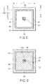
- FIGS. 10 to 14 show the basic structure of the transmission antenna 22.
- the transmission antenna 22 includes a dielectric substrate having a thickness of 1.2 mm and a low dielectric constant (about 3.5), for example, a ground-plane conductor 122 arranged on one surface (back surface in FIGS. 10, 11 ) of the dielectric substrate 121, an unbalanced antenna element 123 in the form of a clockwise rectangular spiral formed as a pattern on the reverse surface (front surface in FIGS. 10, 11 ) of the dielectric substrate 121, and a feed pin 125 with an end thereof connected to the end (feed point) of the antenna element 123 near the spiral center and passed through a hole 122a of the ground-plane conductor 122 along the thickness of the dielectric substrate 121.
- the left-hand circularly polarized radiowave can be emitted from the antenna element 123.
- the surface wave along the surface of the dielectric substrate 121 may be excited and the desired characteristic cannot be obtained due to the effect of the surface wave.
- a plurality of metal posts 130 in the form of pins with one end connected to the ground-plane conductor 122 and the other end extended to the other surface of the dielectric substrate 121 through the dielectric substrate 121, are arranged at predetermined intervals in such positions as to surround the antenna element 123 thereby to make up a cavity structure. Further, the other ends of the metal posts 130 are sequentially shorted along the direction in which they are arranged on the other surface of the dielectric substrate 121, while at the same time arranging a conducting rim 132 extending a predetermined distance toward the antenna element 123 from the connecting point with each metal post 130 thereby to suppress the surface wave.
- the distance (hereinafter referred to as the rim width) by which the conducting rim 132 extends inward from the inner wall of the cavity is designated as L R .
- the rim width L R corresponds to one of several parts of the propagation wavelength of the radiowave in the cavity.
- the plural metal posts 130 are realized, for example, by plating (through-hole plating) on the inner wall of the plural holes formed through the dielectric substrate 121.
- the cavity having this conducting rim 132 is excited by the spiral, so that the surface wave is suppressed, and a circularly polarized antenna having the directivity high in symmetry over a wide band can be obtained.
- a linearly polarized antenna having the wide band characteristic similar to the circularly polarized antenna and having the surface wave suppressed can be obtained also by exciting the cavity with a linearly polarized antenna element such as a bow-tie antenna.
- the transmission antenna 22 shown in FIG. 10 can be used independently for various UWB communication systems.
- the transmission antenna 22 shown in FIG. 10 is itself insufficient in the gain required as a UWB short-range radar or in the case where the beam is required to be reduced, the transmission antenna 22 may be formed in an array.
- a sequential rotation array can be employed by which the cross polarized wave can be suppressed and the polarization characteristic of the antenna as a whole can be improved.
- the sequential rotation array is an array antenna with the same N antenna elements arranged on the same plane, in which each antenna element is arranged sequentially at positions rotated by p ⁇ /N radian around the axis in the direction of emission, while at the same time shifting the phase of power feed to each antenna element by p ⁇ /N radian in accordance with the angle of arrangement thereof, where p is an integer not less than 1 but not more than N-1.
- Non-Patent Document 3 T. Teshirogi et al., "Wideband Circularly Polarized Array Antenna with Sequential Rotation and Phase Shift of Elements," ISAP-85, 024-3, pp. 117-120, 1985 , the cross polarized components are offset and a substantially complete circular polarization characteristic can be obtained for the antenna as a whole even in the case where each antenna element has an incomplete polarization characteristic of a circularly polarized wave (i.e., elliptically polarized wave).
- a circularly polarized wave i.e., elliptically polarized wave
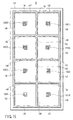
- FIG. 15 shows the configuration of the transmission antenna 22 formed in an array based on the principle described above.
- This transmission antenna 22 includes the antenna elements 123 in an array of two columns and four stages formed on a longitudinally rectangular common dielectric substrate 121' and a ground-plane conductor not shown.
- a feed unit (not shown) for feeding the excitation signal distributively to the plural antenna elements is formed on the ground-plane conductor side of the antenna 22.
- the surface of the dielectric substrate 121' is formed with eight antenna elements 123(1) to 123(8) in two columns and four stages in the form of a right-hand rectangular spiral as in the case of FIG. 10 .
- the antenna elements 123(1) to 123(8) are each surrounded by a cavity formed of plural metal posts 130 arranged with each one end thereof connected to the ground-plane conductor on the one hand, while the other ends of the metal posts 130 are connected along the direction of arrangement thereof by the conducting rim 132' extended by a predetermined distance (corresponding to the rim width LR described above) toward each antenna element 123 from the connecting point of each metal post 130 on the other hand. In this way, the generation of the surface wave of each antenna element is suppressed.
- the transmission antenna 22 described above can be considered to be configured of a resonator by the provision of the conducting rim 132' and the cavity array due to the metal posts 130 on the dielectric substrate 121', which resonator is excited by the circularly polarized antenna elements.
- the resonator has a resonance frequency, at which the input impedance of the antenna is so large that the transmission antenna 22 fails to emit any signal.
- the resonance frequency is determined by the structural parameters of the circularly polarized antenna elements and the resonator.
- the frequency characteristic of the antenna gain of the transmission antenna 22 having the aforementioned configuration develops a deep notch steeply falling in the neighborhood of the resonance frequency.
- this resonance frequency in coincidence with the RR prohibited band (23.6 to 24.0 GHz), for example, the interference with the earth exploration satellite service (EESS) by the short pules wave Pt emitted from the short-range radar using the transmission antenna 22 can be remarkably reduced.
- EESS earth exploration satellite service
- FIG. 16 shows the result of test-producing the transmission antenna 22 having the configuration shown in FIG. 15 and measuring the frequency characteristic of the gain of the right-hand circular polarization (RHCP) component of the main polarized wave and the left-hand circular polarization (LHCP) component of the cross polarized wave of the transmission antenna 22.
- RHCP right-hand circular polarization
- LHCP left-hand circular polarization
- the main polarized wave component has the gain of not less than 13 dBi over the range of 24.5 to 31 GHz, and a steep notch with a fall of about 20 dB from the peak level is generated in the RR prohibited band.
- the frequency generating this notch can be easily rendered to coincide with the RR prohibited band by appropriately selecting the structural parameters of the resonator and/or the spiral antenna.
- the level of radiowave emission to the RR prohibited band can be reduced easily by at least 20 dB in collaboration with the carrier leak reduction technique described above.
- the new spectrum mask in accordance with the FCC recommendation described above can be satisfied.
- the short pulse wave Pt emitted into the space 1 from the transmission antenna 22 having this configuration is reflected from an object 2 in the space 1 and the resulting reflected wave Pr is received by the receiving antenna 41 of the receiving unit 40.
- This receiving antenna 41 can have the same configuration as the transmission antenna 22.
- the circularly polarized radiowave has such a property as to be inverted in the direction of polarized rotation by reflection, and therefore, by setting the polarized rotation of the receiving antenna 41 in the direction opposite to that of the transmission antenna, the secondary reflection component (or more strictly, the even-numbered reflection component) at the receiving antenna 41 can be suppressed for an improved selectivity of the primary reflection component (more strictly, the odd-numbered reflection component). Thus, the false echo generated by the secondary reflection at the receiving antenna 41 can be reduced.
- LNA low-noise amplifier
- the gain of the LNA 42 can be changed by the control unit 62.
- the receiving signal R' limited in band is input to and detected by a detection circuit 44.
- the detection circuit 44 though of various types including the quadrature demodulation type, is assumed to be of square detection type, of which an example is explained below.
- LPF lowpass filter
- the linear multiplier 46 though of several types including the one using a double balanced mixer, is assumed to be of a type configured using the Gilbert mixer for high speed operation.
- the Gilbert mixer as shown in FIG. 17 , has three differential amplifiers 46a, 46b, 46c.
- the first differential amplifier 46a including transistors Q1, Q2, emitter resistors R1, R2 and a constant current source I is differentially supplied with the first signal V1 of the pair of signals V1, V2.
- the second and third differential amplifiers 46b, 46c including transistors Q3, Q4 and transistors Q5, Q6 connected to the load side of the first differential amplifier 46a are supplied with the second signal V2 of the pair of signals V1, V2.
- Vb1, Vb2 and Vb3 designate the bias power supplies for the first, second and third differential amplifiers 46a, 46b and 46c, respectively.
- the linear multiplier 46 making up the Gilbert mixer formed of a plurality of differential amplifiers described above can be configured in a very compact form of a monolithic microwave integrated circuit (MMIC). Further, the local signal is not required to be supplied, and therefore, the power consumption is advantageously small.
- MMIC monolithic microwave integrated circuit
- the baseband signal W obtained from the detection circuit 44 is input to a sample-and-hold circuit 48.
- the sample-and-hold circuit 48 is so configured that the baseband signal W is input to the integrated circuit including a resistor 48a and a capacitor 48b through a switch 48c. As long as a pulse signal P3 from a pulse generator 49 is kept at high level (or low level), the switch 48c is closed and the baseband signal W is integrated, while the switch 48c is opened and the integration result held when the pulse signal P3 falls to low level.
- the pulse generator 49 generates the pulse signal P3 of a predetermined width Td and outputs it to the sample-and-hold circuit 48 each time a receiving trigger signal G' output at least time Ts behind the transmission trigger signal G is received from the control unit 62.
- This receiving unit 40 therefore, executes the receiving process including the process of detecting the reflected wave Pr received before the lapse of a predetermined time T3 from the time of receipt of the receiving trigger signal G'.
- the width Td of the pulse signal P3 can be changed by the control unit 62.
- the signal processing unit 61 based on the signal H obtained by the receiving unit 40, analyzes the object 1a existing in the space 1, and notifies the analysis result to an output device not shown (such as a display or a voice generator) while at the same time notifying the control unit 62 of the information required for the control operation.
- an output device not shown such as a display or a voice generator
- the control unit 62 in accordance with a predetermined schedule for the short-range radar 20 or the processing result of the signal processing unit 61, performs various control operations (variable control of the delay time between the trigger signals G, G', etc.) on at least one of the transmitting unit 21 and the receiving unit 40 and thus causes the short-range radar to investigate the area in the desired range.
- the switch circuit 25d is closed between the input side of the amplifier 25a and the earth line as shown in FIG. 3 to prevent the positive feedback (stop the oscillation).
- the switch circuit 25d is adapted to be closed between the output side of the amplifier 25a and the earth line, i.e. the two ends of the resonator 25b thereby to stop the oscillation.
- the resonator 25b used for the oscillator 25 is not necessarily of LC type but may be configured of transmission path type (such as ⁇ /4 type).
- FIG. 20A is a block diagram showing the general configuration of a second embodiment using the short-range radar and the control method thereof according to the invention.
- FIG. 20A the parts configured similarly to those of the short-range radar according to the first embodiment shown in FIG. 1 described above are designated by the same reference numerals, respectively, and not described again.
- the linear multiplier 46 of square detection type requiring no local signal is employed as the detection circuit 44 of the receiving unit 40.
- a quadrature demodulator 51 of quadrature demodulation type requiring the local signal is employed as the detection circuit 4 of the receiving unit 40.
- this quadrature demodulator 51 of quadrature demodulation type requires the local signal equal in frequency to the receiving signal, and the burst carrier U output from the oscillator 25 of the transmitting unit 21 may be used as such a local signal.
- the output period Tc of the burst carrier U cannot be lengthened greatly in order to suppress the average power of the carrier leak.
- the detection method of quadrature demodulation type using, as the local signal, the burst carrier U output from the oscillator 25 of the transmitting unit 21 can be used.
- the second embodiment therefore, is applicable to a case where the exploration range of the short-range radar is not very long, and has the feature that it can be realized with a simple configuration.
- this second embodiment is not explained here as it can be realized in such a manner that a variable delay unit 50 shown in FIGS. 20B , 20C in a third embodiment described later is omitted and the burst carrier U output from the oscillator 25 of the transmitting unit 21 is input directly as a local signal to the quadrature demodulator 51.
- FIG. 20B is a block diagram showing the general configuration of a third embodiment using the short-range radar and the control method thereof according to this invention.
- FIG. 20B the parts configured similarly to those of the short-range radar according to the first embodiment shown in FIG. 1 described above are designated by the same reference numerals, respectively, and not explained any more.
- the second embodiment described above is applicable to a case in which the exploration range of the short-range radar is not very long, while the third embodiment is used in a case where the exploration range of the short-range radar is long.
- the output period Tc of the burst carrier U output from the oscillator 25 of the transmitting unit 21 is lengthened, thereby posing the problem that the carrier leak is increased.
- the burst carrier U output from the oscillator 25 of the transmitting unit 21 is appropriately delayed by the variable delay unit 50 and applied as a local signal Ur to the quadrature demodulator 51.
- the exploration range of the short-range radar is considered capable of being shifted by controlling the delay amount of the variable delay unit 50.
- the outputs of two systems including the baseband components I, Q from the quadrature demodulator 51 are shown collectively in one system in FIGS. 20A , 20B .
- the outputs of two systems including the baseband components I, Q from the quadrature demodulator 51 are processed by two systems in each subsequent unit of the LPF 47, the sample-and-hold circuit 48 and the A/D converter 60.
- This quadrature demodulator 51 is what is called the quadrature detector having the internal structure shown in FIG. 20C .
- the receiving signal R' from the BRF 43 is divided into two signals having the phase difference of 90° by a phase shifter 51a and input to two mixers 51b, 51c, respectively.
- the outputs of the two mixers 51b, 51c are input to the two LPFs 47a, 47b, respectively.
- the two LPFs 47a, 47b extract the baseband components I, Q and output them to the two sample-and-hold circuits 48a, 48b.
- the baseband components I, Q integrated and held by the sample-and-hold circuits 48a, 48b are converted into digital signals by two A/D converters 60a, 60b, respectively, and supplied to the signal processing unit 61.
- the quadrature demodulator 51 can be used also with a configuration in which the receiving signal R' and the local signal Ur are replaced with each other in FIGS. 20A , B, C.
- the operation similar to the one shown in FIG. 2 is performed at the transmitting end in the manner shown in (a) to (e) of FIG. 21 so that the short pulse wave Pt is emitted into the space.
- the reflected wave Pr is received from the object 1a existing in the space, and the receiving signal R' is input to the quadrature demodulator 51, for example, at the timing shown in (f) of FIG. 21 .
- the signal processing unit 61 executes the process of analyzing the object 1a.
- the carrier signal is output only for a short time only at the timing required for receiving.
- the emission strength of the carrier signal leaking from the receiving end can also be sufficiently reduced.
- variable delay unit 50 is added with the quadrature demodulator 51 as a system configuration. Therefore, a highly sensitive detection process can be realized by a comparatively simple configuration.
- FIG. 22 is a block diagram showing the general configuration of a fourth embodiment using the short-range radar and the control method thereof according to this invention.
- FIG. 22 the parts configured similarly to those of the short-range radar according to the first embodiment shown in FIG. 1 described above are designated by the same reference numerals, respectively, and not explained any more.
- the short-range radar 20 employs a configuration in which the frequency of a local signal Lvco output continuously to the quadrature demodulator 51 from a VCO 56 is locked by the burst carrier U and thus stabilized using a phase-locked loop (PLL) configuration including frequency dividers 54, 55 having the same frequency dividing ratio, a voltage-controlled transmitter (VCO) 56, a phase comparator 57 and a hold circuit 58.
- PLL phase-locked loop
- the frequency dividers 54, 55 may be omitted.
- the hold circuit 58 upon receipt of the second pulse P2, applies the output signal of the phase comparator 57 to the VCO 56 and locks the phase and frequency of the local signal Lvco through the burst carrier U for a predetermined time (for example, from rise to fall of the second pulse P2) when the burst carrier U is input and the frequency thereof stabilized.
- a predetermined time for example, from rise to fall of the second pulse P2
- the frequency shift of the local signal Lvco in the free-running state is minimized by supplying the VCO 56 with the output signal of the phase comparator 57 held immediately before the end of the particular predetermined period.
- the local signal Lvco is a continuous wave, and therefore, the signal extraction in the exploration range is carried out by the sample-and-hold circuit 48.
- the outputs of the two systems including the baseband components I, Q from the quadrature demodulator 51 are processed subsequently by two systems also in each of the LPFs 47a, 47b, the sample-and-hold circuits 48a, 48b and the A/D converters 60a, 60b.
- the operation similar to that shown in FIG. 2 is performed at the transmitting end as shown in (a) to (e) of FIG. 23 , so that the short pulse wave Pt is emitted into the space 1, the reflected wave Pr from the object la existing in the space 1 is received, and at the timing as shown in (f) of FIG. 23 , for example, the reflected signal R' is input to the quadrature demodulator 51.
- the frequency of the local signal Lvco input to the quadrature demodulator 51 from the VCO 56 is locked during the period when the second pulse P2 is input, and after end of this period, held by holding the control signal to the VCO 56, so that the frequency of the local signal Lvco is held in substantially stable state.
- This stability holding time is assumed to be sufficiently long as compared with the width Tc of the first pulse P1 and longer than the time corresponding to the longest exploration range.
- the exploration can be continuously carried out for a long time (i.e. for a long range) from the emission timing of the short pulse wave Pt.
- the locked period can be set regardless of the output period of the second pulse.
- the pulse signal for specifying the locked period is generated separately from the control unit 62.
- the quadrature demodulator 51 is used as the detection circuit 44 as in the short-range radar 20 shown in FIGS. 20A , B, C and 22, the local signal is required disadvantageously.
- the dynamic range thereof is twice wider in terms of the value dB than the square detection method, so that the detection is possible even for the small level of the input signal. This is effective for the short-range radar requiring a highly sensitive receiving operation.
- a short-range radar and a control method thereof can be provided in which the RR prohibited band and the SRD band are not interfered with while complying with the specified spectrum mask with an inexpensive configuration.
Landscapes
- Engineering & Computer Science (AREA)
- Radar, Positioning & Navigation (AREA)
- Remote Sensing (AREA)
- Computer Networks & Wireless Communication (AREA)
- Physics & Mathematics (AREA)
- General Physics & Mathematics (AREA)
- Signal Processing (AREA)
- Radar Systems Or Details Thereof (AREA)
Applications Claiming Priority (2)
| Application Number | Priority Date | Filing Date | Title |
|---|---|---|---|
| JP2006116729 | 2006-04-20 | ||
| PCT/JP2007/054074 WO2007122873A1 (fr) | 2006-04-20 | 2007-03-02 | Radar à impulsions brèves et procédé de contrôle dudit radar |
Publications (1)
| Publication Number | Publication Date |
|---|---|
| EP2009461A1 true EP2009461A1 (fr) | 2008-12-31 |
Family
ID=38624789
Family Applications (1)
| Application Number | Title | Priority Date | Filing Date |
|---|---|---|---|
| EP07715168A Withdrawn EP2009461A1 (fr) | 2006-04-20 | 2007-03-02 | Radar à impulsions brèves et procédé de contrôle dudit radar |
Country Status (5)
| Country | Link |
|---|---|
| US (1) | US7812760B2 (fr) |
| EP (1) | EP2009461A1 (fr) |
| JP (1) | JPWO2007122873A1 (fr) |
| CN (1) | CN101375177B (fr) |
| WO (1) | WO2007122873A1 (fr) |
Cited By (1)
| Publication number | Priority date | Publication date | Assignee | Title |
|---|---|---|---|---|
| EP4160267A1 (fr) * | 2012-06-25 | 2023-04-05 | Veoneer US, LLC | Radar à monopulse à deux canaux destiné à une détection tridimensionnelle |
Families Citing this family (27)
| Publication number | Priority date | Publication date | Assignee | Title |
|---|---|---|---|---|
| JP5390780B2 (ja) * | 2008-03-14 | 2014-01-15 | 古河電気工業株式会社 | パルス発生方法、パルス発生装置およびレーダ装置 |
| US8441324B2 (en) * | 2008-05-13 | 2013-05-14 | Freescale Semiconductor, Inc. | Voltage-controlled oscillator and radar system |
| DE102008044355A1 (de) * | 2008-12-04 | 2010-06-10 | Robert Bosch Gmbh | Modulares Radarsystem |
| JP4752932B2 (ja) * | 2009-02-25 | 2011-08-17 | 株式会社デンソー | 送信装置、受信装置、及び送受信装置 |
| US8237604B2 (en) * | 2009-03-06 | 2012-08-07 | Tialinx, Inc. | Virtual beam forming in ultra wideband systems |
| US8098193B2 (en) * | 2009-11-05 | 2012-01-17 | Honeywell International Inc. | Digitally controlled UWB millimeter wave radar |
| CN101968541B (zh) * | 2010-09-17 | 2012-07-11 | 国营红林机械厂 | 脉冲超宽带测距系统 |
| CN104105981B (zh) | 2011-10-19 | 2016-04-20 | B·苏博拉曼亚 | 定向速度和距离传感器 |
| CN102499652A (zh) * | 2011-10-27 | 2012-06-20 | 中国人民解放军第四军医大学 | 一种用于监测生命信号的微功率雷达 |
| EP2695297B1 (fr) | 2012-05-02 | 2015-07-08 | Institute of Electronics and Computer Science | Raidisseur de fronts d'impulsions à bande ultra-large pour l'excitation d'une antenne symétrique |
| US11004337B2 (en) * | 2012-12-28 | 2021-05-11 | Balu Subramanya | Advanced parking management system |
| CN103105606B (zh) * | 2013-01-18 | 2015-02-11 | 中国人民解放军海军航空工程学院 | 一种脉冲无源双基地雷达接收相干处理方法 |
| EP3044723A4 (fr) * | 2013-09-12 | 2017-05-03 | Dockon AG | Système amplificateur détecteur logarithmique destiné à être utilisé comme récepteur sélectif à haute sensibilité sans conversion de fréquence |
| JP6377000B2 (ja) * | 2015-03-25 | 2018-08-22 | パナソニック株式会社 | レーダ装置 |
| EP3561538B1 (fr) * | 2016-12-22 | 2025-11-12 | Furukawa Electric Co., Ltd. | Dispositif de génération d'impulsions et procédé de réglage de sortie correspondant |
| JP6734405B2 (ja) * | 2017-01-27 | 2020-08-05 | 株式会社日立製作所 | 移動体検知システム |
| JP6717254B2 (ja) * | 2017-04-19 | 2020-07-01 | 株式会社デンソー | レーダ信号処理器及びレーダシステム |
| DE102018117688A1 (de) * | 2017-08-18 | 2019-02-21 | Infineon Technologies Ag | Radar-Frontend mit HF-Oszillator-Überwachung |
| DE102018200763A1 (de) * | 2018-01-18 | 2019-07-18 | Robert Bosch Gmbh | Vorrichtung und Verfahren zum Verarbeiten eines Eingabesignals und Radarvorrichtung |
| US10983205B2 (en) * | 2018-08-02 | 2021-04-20 | GM Global Technology Operations LLC | Redundant frequency modulators in radar system |
| EP3703269B1 (fr) * | 2019-02-26 | 2022-06-08 | Nxp B.V. | Alignement de phase d'une horloge de contrôleur sur un champ |
| US12445109B2 (en) | 2019-07-31 | 2025-10-14 | QXONIX Inc. | Structures, acoustic wave resonators, layers, devices and systems |
| WO2021021736A1 (fr) | 2019-07-31 | 2021-02-04 | QXONIX Inc. | Systèmes, dispositifs et structures de résonateur et réflecteur à ondes acoustiques de volume (baw) |
| US12451860B2 (en) | 2019-07-31 | 2025-10-21 | QXONIX Inc. | Structures, acoustic wave resonators, devices and systems |
| US12431861B2 (en) | 2019-07-31 | 2025-09-30 | Qxoniix Inc. | Layers, structures, acoustic wave resonators, devices and systems |
| DE102020206800B4 (de) * | 2020-05-29 | 2022-12-15 | Infineon Technologies Ag | Phasenschieberkonzept und Radartransmitterkonzept |
| CN118678447B (zh) * | 2024-08-21 | 2024-10-25 | 浙江大信科技股份有限公司 | 一种基于uwb基站抗干扰精确定位的智能方法 |
Family Cites Families (18)
| Publication number | Priority date | Publication date | Assignee | Title |
|---|---|---|---|---|
| US3945012A (en) * | 1966-11-07 | 1976-03-16 | Rockwell International Corporation | Wide band pulsed energy system |
| US3603991A (en) * | 1969-10-30 | 1971-09-07 | Raytheon Co | Radar frequency spectrum control circuit |
| SE336816B (fr) * | 1969-11-06 | 1971-07-19 | Ericsson Telefon Ab L M | |
| US3688214A (en) * | 1970-01-23 | 1972-08-29 | Harry Goldie | Means for generating narrow microwave pulses |
| US3706095A (en) * | 1970-11-23 | 1972-12-12 | Raytheon Co | Signal processor |
| US4123755A (en) * | 1975-10-10 | 1978-10-31 | William Fishbein | Radar interference reduction |
| US4320399A (en) * | 1980-10-09 | 1982-03-16 | Westinghouse Electric Corp. | Microwave pulse spectrum control |
| US4450444A (en) * | 1981-05-29 | 1984-05-22 | The United States Of America As Represented By The Secretary Of The Navy | Stepped frequency radar target imaging |
| JPS60196018A (ja) | 1984-03-17 | 1985-10-04 | Nec Corp | 低消費電力送受信装置 |
| JPS63122981A (ja) | 1986-11-13 | 1988-05-26 | Nec Corp | 測距方式 |
| US5361070B1 (en) * | 1993-04-12 | 2000-05-16 | Univ California | Ultra-wideband radar motion sensor |
| US5543799A (en) * | 1994-09-02 | 1996-08-06 | Zircon Corporation | Swept range gate radar system for detection of nearby objects |
| US6191724B1 (en) * | 1999-01-28 | 2001-02-20 | Mcewan Thomas E. | Short pulse microwave transceiver |
| US6414627B1 (en) * | 1999-10-12 | 2002-07-02 | Mcewan Technologies, Llc | Homodyne swept-range radar |
| FR2818385B1 (fr) * | 2000-12-15 | 2004-06-04 | Thomson Csf | Radar large bande et modulateur, notamment pour commuter des ondes hyperfrequence sur une tres courte duree |
| DE10104022A1 (de) * | 2001-01-31 | 2002-08-01 | Bosch Gmbh Robert | Radareinrichtung und Verfahren zum Codieren einer Radareinrichtung |
| EP1610150B1 (fr) | 2001-04-03 | 2016-06-22 | Mitsubishi Electric Information Technology Centre Europe B.V. | Procédé et dispositif de détection d'un signal cible et système de détection d'obstacles |
| US7450058B2 (en) | 2004-05-31 | 2008-11-11 | Anritsu Corporation | Radar oscillator capable of preventing leak of oscillation output |
-
2007
- 2007-03-02 EP EP07715168A patent/EP2009461A1/fr not_active Withdrawn
- 2007-03-02 CN CN2007800008406A patent/CN101375177B/zh not_active Expired - Fee Related
- 2007-03-02 US US11/989,274 patent/US7812760B2/en not_active Expired - Fee Related
- 2007-03-02 JP JP2008511998A patent/JPWO2007122873A1/ja active Pending
- 2007-03-02 WO PCT/JP2007/054074 patent/WO2007122873A1/fr not_active Ceased
Non-Patent Citations (1)
| Title |
|---|
| See references of WO2007122873A1 * |
Cited By (1)
| Publication number | Priority date | Publication date | Assignee | Title |
|---|---|---|---|---|
| EP4160267A1 (fr) * | 2012-06-25 | 2023-04-05 | Veoneer US, LLC | Radar à monopulse à deux canaux destiné à une détection tridimensionnelle |
Also Published As
| Publication number | Publication date |
|---|---|
| JPWO2007122873A1 (ja) | 2009-09-03 |
| CN101375177B (zh) | 2012-07-18 |
| US7812760B2 (en) | 2010-10-12 |
| WO2007122873A1 (fr) | 2007-11-01 |
| CN101375177A (zh) | 2009-02-25 |
| US20090256740A1 (en) | 2009-10-15 |
Similar Documents
| Publication | Publication Date | Title |
|---|---|---|
| EP2009461A1 (fr) | Radar à impulsions brèves et procédé de contrôle dudit radar | |
| AU2005227368B2 (en) | Transponder, including transponder system | |
| US7710311B2 (en) | Short range radar small in size and low in power consumption and controlling method thereof | |
| US6414627B1 (en) | Homodyne swept-range radar | |
| US6946989B2 (en) | Transponder, including transponder system | |
| US8115673B1 (en) | Self-oscillating UWB emitter-detector | |
| US10746862B2 (en) | Short range radar cohabitation | |
| US8854254B2 (en) | Ultra-wideband short-pulse radar with range accuracy for short range detection | |
| EP1843170A1 (fr) | Radar ulb a impulsions courtes | |
| JP3021160B2 (ja) | パルスドップラーレーダの送受信部 | |
| US20070194978A1 (en) | Uwb short-range radar | |
| CN111638504B (zh) | 连续波雷达前端 | |
| US20080246650A1 (en) | Short Range Radar and Method of Controlling the Same | |
| EP1736795A1 (fr) | Radar a impulsions courtes et procede de controle associe | |
| JP2008249498A (ja) | レーダ装置 | |
| Ju et al. | Design and implementation of a hybrid digital and RF front‐end module for 24‐GHz intelligent transport system pulse‐doppler radar | |
| US20060125683A1 (en) | Radar sensor and method for operating a radar sensor | |
| Al-Alem | CHIP LEVEL IMPLEMENTATION OF A DIGITAL | |
| Huettner et al. | A low cost Ultra-Wide-Band Pulse Radar in a guided wave gauging application | |
| Kim et al. | Design and implementation of a hybrid UWB pulse generator for automotive Radar | |
| Kandar et al. | Development of an imaging radar instrumentation system using DS-UWB wireless technology | |
| Han et al. | A multipulse transmitter for UWB radar and communication systems | |
| Han et al. | On the development of a low-cost compact planar integrated-circuit sampling receiver for UWB sytems | |
| Al-Alem | AUS Repository | |
| Teshirogi et al. | UWB radar RF front-end to mitigate impacts on EESS and radio astronomy |
Legal Events
| Date | Code | Title | Description |
|---|---|---|---|
| PUAI | Public reference made under article 153(3) epc to a published international application that has entered the european phase |
Free format text: ORIGINAL CODE: 0009012 |
|
| 17P | Request for examination filed |
Effective date: 20080123 |
|
| AK | Designated contracting states |
Kind code of ref document: A1 Designated state(s): AT BE BG CH CY CZ DE DK EE ES FI FR GB GR HU IE IS IT LI LT LU LV MC MT NL PL PT RO SE SI SK TR |
|
| AX | Request for extension of the european patent |
Extension state: AL BA HR MK RS |
|
| DAX | Request for extension of the european patent (deleted) | ||
| RBV | Designated contracting states (corrected) |
Designated state(s): DE FR GB IT |
|
| STAA | Information on the status of an ep patent application or granted ep patent |
Free format text: STATUS: THE APPLICATION HAS BEEN WITHDRAWN |
|
| 18W | Application withdrawn |
Effective date: 20140402 |