EP2009660A2 - Verfahren zum Herstellen eines Tafelschalters und Tafelschalter - Google Patents
Verfahren zum Herstellen eines Tafelschalters und Tafelschalter Download PDFInfo
- Publication number
- EP2009660A2 EP2009660A2 EP08011590A EP08011590A EP2009660A2 EP 2009660 A2 EP2009660 A2 EP 2009660A2 EP 08011590 A EP08011590 A EP 08011590A EP 08011590 A EP08011590 A EP 08011590A EP 2009660 A2 EP2009660 A2 EP 2009660A2
- Authority
- EP
- European Patent Office
- Prior art keywords
- insulating film
- contact
- moving contact
- moving
- adhesive layer
- Prior art date
- Legal status (The legal status is an assumption and is not a legal conclusion. Google has not performed a legal analysis and makes no representation as to the accuracy of the status listed.)
- Granted
Links
- 238000004519 manufacturing process Methods 0.000 title claims abstract description 46
- 239000012790 adhesive layer Substances 0.000 claims abstract description 45
- 238000000034 method Methods 0.000 claims abstract description 31
- 239000010410 layer Substances 0.000 claims abstract description 5
- 230000001678 irradiating effect Effects 0.000 claims description 6
- 239000000463 material Substances 0.000 description 20
- 238000010030 laminating Methods 0.000 description 5
- 239000000853 adhesive Substances 0.000 description 3
- 230000001070 adhesive effect Effects 0.000 description 3
- 238000010586 diagram Methods 0.000 description 3
Images









Classifications
-
- H—ELECTRICITY
- H01—ELECTRIC ELEMENTS
- H01H—ELECTRIC SWITCHES; RELAYS; SELECTORS; EMERGENCY PROTECTIVE DEVICES
- H01H13/00—Switches having rectilinearly-movable operating part or parts adapted for pushing or pulling in one direction only, e.g. push-button switch
- H01H13/02—Details
- H01H13/26—Snap-action arrangements depending upon deformation of elastic members
- H01H13/48—Snap-action arrangements depending upon deformation of elastic members using buckling of disc springs
-
- H—ELECTRICITY
- H01—ELECTRIC ELEMENTS
- H01H—ELECTRIC SWITCHES; RELAYS; SELECTORS; EMERGENCY PROTECTIVE DEVICES
- H01H13/00—Switches having rectilinearly-movable operating part or parts adapted for pushing or pulling in one direction only, e.g. push-button switch
- H01H13/70—Switches having rectilinearly-movable operating part or parts adapted for pushing or pulling in one direction only, e.g. push-button switch having a plurality of operating members associated with different sets of contacts, e.g. keyboard
- H01H13/88—Processes specially adapted for manufacture of rectilinearly movable switches having a plurality of operating members associated with different sets of contacts, e.g. keyboards
-
- H—ELECTRICITY
- H01—ELECTRIC ELEMENTS
- H01H—ELECTRIC SWITCHES; RELAYS; SELECTORS; EMERGENCY PROTECTIVE DEVICES
- H01H2205/00—Movable contacts
- H01H2205/016—Separate bridge contact
- H01H2205/024—Means to facilitate positioning
- H01H2205/026—Adhesive sheet
-
- H—ELECTRICITY
- H01—ELECTRIC ELEMENTS
- H01H—ELECTRIC SWITCHES; RELAYS; SELECTORS; EMERGENCY PROTECTIVE DEVICES
- H01H2215/00—Tactile feedback
- H01H2215/034—Separate snap action
- H01H2215/036—Metallic disc
-
- H—ELECTRICITY
- H01—ELECTRIC ELEMENTS
- H01H—ELECTRIC SWITCHES; RELAYS; SELECTORS; EMERGENCY PROTECTIVE DEVICES
- H01H2229/00—Manufacturing
- H01H2229/02—Laser
-
- H—ELECTRICITY
- H01—ELECTRIC ELEMENTS
- H01H—ELECTRIC SWITCHES; RELAYS; SELECTORS; EMERGENCY PROTECTIVE DEVICES
- H01H2229/00—Manufacturing
- H01H2229/034—Positioning of layers
-
- Y—GENERAL TAGGING OF NEW TECHNOLOGICAL DEVELOPMENTS; GENERAL TAGGING OF CROSS-SECTIONAL TECHNOLOGIES SPANNING OVER SEVERAL SECTIONS OF THE IPC; TECHNICAL SUBJECTS COVERED BY FORMER USPC CROSS-REFERENCE ART COLLECTIONS [XRACs] AND DIGESTS
- Y10—TECHNICAL SUBJECTS COVERED BY FORMER USPC
- Y10T—TECHNICAL SUBJECTS COVERED BY FORMER US CLASSIFICATION
- Y10T156/00—Adhesive bonding and miscellaneous chemical manufacture
- Y10T156/10—Methods of surface bonding and/or assembly therefor
- Y10T156/1052—Methods of surface bonding and/or assembly therefor with cutting, punching, tearing or severing
- Y10T156/108—Flash, trim or excess removal
-
- Y—GENERAL TAGGING OF NEW TECHNOLOGICAL DEVELOPMENTS; GENERAL TAGGING OF CROSS-SECTIONAL TECHNOLOGIES SPANNING OVER SEVERAL SECTIONS OF THE IPC; TECHNICAL SUBJECTS COVERED BY FORMER USPC CROSS-REFERENCE ART COLLECTIONS [XRACs] AND DIGESTS
- Y10—TECHNICAL SUBJECTS COVERED BY FORMER USPC
- Y10T—TECHNICAL SUBJECTS COVERED BY FORMER US CLASSIFICATION
- Y10T29/00—Metal working
- Y10T29/49—Method of mechanical manufacture
- Y10T29/49002—Electrical device making
- Y10T29/49105—Switch making
-
- Y—GENERAL TAGGING OF NEW TECHNOLOGICAL DEVELOPMENTS; GENERAL TAGGING OF CROSS-SECTIONAL TECHNOLOGIES SPANNING OVER SEVERAL SECTIONS OF THE IPC; TECHNICAL SUBJECTS COVERED BY FORMER USPC CROSS-REFERENCE ART COLLECTIONS [XRACs] AND DIGESTS
- Y10—TECHNICAL SUBJECTS COVERED BY FORMER USPC
- Y10T—TECHNICAL SUBJECTS COVERED BY FORMER US CLASSIFICATION
- Y10T29/00—Metal working
- Y10T29/49—Method of mechanical manufacture
- Y10T29/49002—Electrical device making
- Y10T29/49117—Conductor or circuit manufacturing
-
- Y—GENERAL TAGGING OF NEW TECHNOLOGICAL DEVELOPMENTS; GENERAL TAGGING OF CROSS-SECTIONAL TECHNOLOGIES SPANNING OVER SEVERAL SECTIONS OF THE IPC; TECHNICAL SUBJECTS COVERED BY FORMER USPC CROSS-REFERENCE ART COLLECTIONS [XRACs] AND DIGESTS
- Y10—TECHNICAL SUBJECTS COVERED BY FORMER USPC
- Y10T—TECHNICAL SUBJECTS COVERED BY FORMER US CLASSIFICATION
- Y10T29/00—Metal working
- Y10T29/49—Method of mechanical manufacture
- Y10T29/49002—Electrical device making
- Y10T29/49117—Conductor or circuit manufacturing
- Y10T29/49124—On flat or curved insulated base, e.g., printed circuit, etc.
- Y10T29/49155—Manufacturing circuit on or in base
-
- Y—GENERAL TAGGING OF NEW TECHNOLOGICAL DEVELOPMENTS; GENERAL TAGGING OF CROSS-SECTIONAL TECHNOLOGIES SPANNING OVER SEVERAL SECTIONS OF THE IPC; TECHNICAL SUBJECTS COVERED BY FORMER USPC CROSS-REFERENCE ART COLLECTIONS [XRACs] AND DIGESTS
- Y10—TECHNICAL SUBJECTS COVERED BY FORMER USPC
- Y10T—TECHNICAL SUBJECTS COVERED BY FORMER US CLASSIFICATION
- Y10T29/00—Metal working
- Y10T29/49—Method of mechanical manufacture
- Y10T29/49002—Electrical device making
- Y10T29/49117—Conductor or circuit manufacturing
- Y10T29/49204—Contact or terminal manufacturing
Definitions
- Devices and methods consistent with the present invention relate to switches and their manufacture and, more particularly, to a panel switch for use in electronic equipment, and methods of manufacturing the same.
- Japanese Patent Publication No. 2003-100165A describes a related art sheet-shaped panel switch.
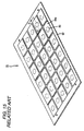
- Fig. 15 shows a perspective view of a related art panel switch and Fig. 16 shows an enlarged sectional view taken on line C - C in Fig. 15 .
- the related art panel switch 51 includes a wiring board 52; a plurality of moving contacts 53 arranged on the wiring board 52; and a.plurality of insulating film pieces 54a which are attached onto the wiring board 52 in such a manner that they cover the individual moving contacts 53.
- a stationary contact 55 is provided for each of the plurality of moving contacts 53.
- the plurality of stationary contacts 55 are respectively provided by means of printing in a plurality of portions forming a switch portion on a surface of the sheet-shaped insulating film.
- Each stationary contact 55 includes an outside electrode 55a formed into a substantially annular shape and a central electrode 55b provided in a central portion surrounded by the outside electrode 55a.
- the outside electrode 55a and the central electrode 55b are respectively connected to a connector terminal portion which is electrically connected to an external circuit.
- Each moving contact 53 includes a lower side contact portion 53a which is formed as a circular-plate-shaped body formed out of an elastic metallic sheet, the shape of which is swelled into a dome-shape, so that it can be arranged on the outside electrode 55a of the wiring board 52; and an apex portion 53b arranged being opposed to the central electrode 55b.
- the plurality of moving contacts 53 are arranged on the wiring board 52 corresponding to the plurality of stationary contacts 55.
- Each insulating film piece 54a is formed by a flexible sheet-shaped insulating film that is divided into a plurality of sections which correspond to the plurality of moving contacts 53 by being cut into a predetermined size.
- an adhesive layer 56 (shown in Fig. 16 ) is provided on one side, i.e., an inside, of the insulating film piece 54a.
- the insulating film piece 54a is attached onto the wiring board 52 by an adhesive force of the adhesive layer 56 which adheres the insulating film piece 54a to the moving contact 53.
- a pushing force is not given to the panel switch 51, the moving contact 53, being formed into a dome-shape, is swelled to the insulating film piece 54a side.
- the apex portion 53b of the moving contact 53 is separated from the central electrode 55b, and a state of switch-off is maintained. I.e., the switch is not conducting.
- Fig. 16 shows the related art panel switch 51 in the state of switch-off.
- the apex portion 53b of the moving contact 53 is returned to the initial position together with the insulating film piece 54 by an elastic returning force of the moving contact 53. Accordingly, the apex portion 53b is separated from the central electrode 55b again and the switch is put into a state of switch-off.
- the switch forming material M includes an insulating film 54, an adhesive layer 56, and a separator 52A.
- the adhesive layer 56 is provided on one side of the insulating film 54, and the separator 52A is provided on the other side of the adhesive layer 56.
- the insulating film 54 has a size capable of being divided into the plurality of insulating film pieces 54a.
- the insulating film 54 and the adhesive layer 56 of the switch forming material M are cut into a predetermined size by using a metallic die (not shown). Thus, a plurality of divided insulating film pieces 54a are obtained.
- the switch forming material M is inverted so that the separator 52A is located on the upper side and the insulating film pieces 54a are set at predetermined positions on a jig 57 in order.
- the separator 52A is removed as shown in Fig. 18 .
- the plurality of moving contacts 53 which are turned upside down, are arranged and made to adhere onto the insulating film pieces 54a so that the apex portion 53b of the dome-shaped moving contact 53 can be made to adhere onto the adhesive layer 56.
- An outside dimension of the moving contact 53 is set to be smaller than that of each insulating film piece 54a. Therefore, the moving contact 53 is covered with the corresponding insulating film piece 54a.
- the wiring board 52 is set on the plurality of moving contacts 53 and, the plurality of moving contacts 53 are adhered and fixed to the wiring board 52. It is also possible to use a separator 52B in place of the wiring board 52.
- two positioning pins 58 are arranged on the right and two positioning pins 58 are arranged on the left so as to be protruded from the jig 57. In other words, four positioning pins 58 in total are protruded from the jig 57.
- the positioning pins 58 provided on the jig 57 are inserted into positioning holes 59 provided on the wiring board 52, so that adhesion can be made under the condition that the insulating film pieces are properly positioned.
- an unnecessary portion of the wiring board 52 is removed by being cut off.
- the insulating film pieces 54a are removed from the jig 57, and the related art manufacturing process of the related art panel switch 51 is completed.
- the above-described related art panel switch and related art manufacturing process has a number of disadvantages.
- a profile of the insulating film piece 54a is changed, it is necessary to also change the metallic mold. Accordingly, this results in increased expenses and increased time for manufacturing.
- the touch and feel of the related art panel switch is controlled by the dome-shaped moving contact, and accordingly, there is little variation possible in the touch and feel.
- Exemplary embodiments of the present invention address the above disadvantages and other disadvantages not described above.
- the present invention is not required to overcome the disadvantages described above, and thus, an exemplary embodiment of the present invention may not overcome any of the problems described above.
- a method of manufacturing a panel switch comprising a moving contact sticking operation in which a swelled apex portion of a dome-shaped moving contact is adhered onto an adhesive layer formed on one side of an insulating film; an insulating film sticking operation in which the insulating film is adhered onto a base member having a stationary contact corresponding to the moving contact so as to fix the moving contact to the base member; and an excess film removing operation in which a laser beam is irradiated onto the insulating film which is adhered to the base member so as to cut off and remove an excess portion of the insulating film.
- a panel switch comprising a base layer comprising a stationary contact; a first contact portion comprising a first insulating film; an adhesive layer applied to a side of the first insulating film; and a moving contact comprising an apex portion, the apex portion being adhered to the adhesive layer of the first insulating film; and a second contact portion comprising a second insulating film; an adhesive layer applied to a side of the second insulating film; and a moving contact comprising an apex portion, the apex portion being adhered to the adhesive layer of the second insulating film, wherein the first contact portion is adhered to the base member, and the second contact portion is adhered to the first contact portion, such that the moving contact of the first contact portion, the moving contact of the second contact portion, and the stationary contact are aligned with each other in a direction orthogonal to a surface of the base member.
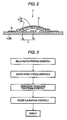
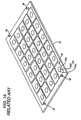
- a panel switch 1 includes a wiring board (base member) 2 having a plurality of stationary contacts 5; a plurality of moving contacts 3, arranged on the wiring board 2; and a plurality of insulating film pieces 4a attached onto the wiring board 2 so as to respectively cover the moving contacts 3.
- Each moving contact 3 is made from a swelled circular-plate-shaped body formed out of an elastic metallic sheet.
- the shape of the swelled circular-plate shaped body is a dome-shape.
- the moving contact 3 includes a lower side contact portion 3a which is formed into a size so that the lower side contact portion 3a can be arranged on the outside electrode 5a of the wiring board 2, and an apex portion 3b arranged so as to be opposed to the central electrode 5b.
- a plurality of moving contacts 3 are arranged on the wiring board 2 corresponding to a plurality of stationary contacts 5.
- the panel switch 1 has 30 moving contacts 3.
- this number of contacts is only exemplary, and the present inventive concept applies equally to a panel switch 1 having any number of switches.
- Each insulating film piece 4a is formed when a flexible sheet-shaped insulating film is divided by being cut to a certain size.
- the insulating film piece 4a functions as a cover tape for covering the moving contact 3.
- an adhesive layer 6 (shown in Fig. 2 ) is provided on one side, e.g., an inside, of the insulating film piece 4a.
- the insulating film piece 4a together with the moving contact 3 is attached onto the wiring board 2 by an adhesive force of the adhesive layer 6.
- the moving switch 3 is swelled upward, as shown in Fig. 2 .
- the moving switch 3 is swelled like a dome-shape onto the insulating film 4a side and the apex portion 3b of the moving contact 3 is separated from a surface of the central electrode 5b. Therefore, the central electrode 5b does not conduct with the outside electrode 5a, and the moving contact 3 is maintained in a state of switch-off.
- the insulating film piece 4a is operated by being pushed towards the wiring board 2, i.e., in a direction roughly orthogonal to the wiring board 2, the insulating film piece 4a and the moving contact 3 are pressed orthogonally to the dome-shape. Therefore, the apex portion 3b of the moving contact 3 comes into contact with the central electrode 5b. Accordingly, the central electrode 5b is brought into a conducting condition with the outside electrode 5a, and the moving contact 3 is put into a state of switch-on.
- the apex portion 3b of the moving contact 3 is raised and returned to the initial dome-shape position together with the insulating film piece 4a by the elastic returning force of the moving contact 3.
- the apex portion 3b is separated from the central electrode 5b again and the moving contact 3 is changed over to a state of switch-off.
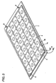
- FIG. 3 is a process block diagram showing a procedure of the manufacturing method according to a first exemplary embodiment of the present invention.
- the manufacturing method according to the first exemplary embodiment of the present invention includes an insulating film preparing operation A, a moving contact sticking operation B, an insulating film sticking operation C,; and an excess film removing step D.
- the operations A to D will now be described in detail.
- a sheet-shaped switch forming material M is prepared.
- the switch forming material M comprises an insulating film 4, an adhesive layer 6, and a separator 2A.
- the adhesive layer 6 is provided on one side of the insulating film 4, and the separator 2A is stuck and fixed onto the adhesive layer 6.
- the switch forming material M is set so that the separator 2A can be directed upward, i.e., away from the jig, and the insulating film 4 on the lower face side of the switch forming material M is set and stuck onto the jig 7. In this way, the switch forming material M is fixed onto the jig 7.
- four positioning pins 8 are provided such that the four positioning pins 8 protrude from the jig 7.
- two positioning pins are arranged on the right side and two positioning pins are arranged on the left side of the jig 7. Accordingly, when the switch forming material M is arranged on the jig 7, the switch forming material M can be accurately positioned and fixed by the pairs of pins 8. In other words, the switch forming material M is placed within the four protruding positioning pins 8 and the switch forming material M is held in between the four protruding positioning pins 8 by friction.
- the wiring board 2 is formed with positioning holes 9 for arranging and fixing the wiring board 2 onto the jig 7.
- the insulating film 4 is formed from a film sheet and the size of the insulating film sheet is sufficiently large so that a desired number of sheets of insulating film pieces 4a can be obtained.
- the insulating film sheet is large enough to provide 30 insulating film pieces 4a.
- an area of the insulating film 4 is approximately half of an area of the insulating film used to produce the related art panel switch since the laser processing requires smaller area of an excess portion 4b.
- the process then proceeds to the moving contact sticking operation B.
- the separator 2A stuck onto the adhesive layer 6 of the insulating film 4 is removed.
- the moving contacts 3 are arranged and fixed onto a plurality of portions of the adhesive layer 6 on which the insulating film pieces 4a described later are scheduled to be formed.
- the moving contacts 3 are turned upside down before being arranged and stuck to the adhesive layer 6 such that the apex portions 3b of the dome-shaped moving contacts 3, which are shown by one-dotted chain lines in Fig. 8C , can be stuck and fixed at desired positions on the insulating film 4.
- a number of moving contacts 3 are respectively stuck and arranged at a plurality of positions on the insulating film 4.
- the number of moving contacts 3 and their positions on the insulating film 4 may be predetermined.
- An outside dimension of each moving contact 3 is set to be smaller than an outside dimension of the insulating film piece 4a which corresponds to the moving contact 3. Therefore, each moving contact 3 is covered with a corresponding insulating film piece 4a.
- a sheet of wiring board 2 is set on the plurality of moving contacts 3.
- a sheet of separator 2B may be used in place of the wiring board 2.
- Positioning holes 9 corresponding to the positioning pins 8 of the jig 7 are formed on the wiring board 2. Therefore, when the positioning pins 8 are inserted into and engaged with the positioning holes 9, the wiring board 2 can be accurately positioned with respect to the jig 7.
- the insulating film 4 and the wiring board 2 are removed from the jig 7 together with the moving contacts 3. Successively, as shown in Fig. 6 , while the dome-shapes of the moving contacts 3 are being maintained, the insulating film 4 and the wiring board 2 are closely contacted with each other. In other words, the areas of the insulating film 4 around the moving contacts 3 are pressed to the wiring board 2 while the dome-shape of the moving contacts 3 is maintained so that the areas of the insulating film 4 around the moving contacts 3 are adhered to the wiring board 2. As a result, the insulating film 4 is strongly stuck and fixed onto a surface of the wiring board 2 by an adhesive force of the adhesive layer 6.
- the moving contacts 3 are also fixed and held at the desired positions on the wiring board 2. That is the moving contacts 3 are also fixed and held at the outside electrodes 5a of the stationary contacts 5. Accordingly, a partially fabricated product (1) comprising the moving contacts 3 is formed (see Fig. 8D ).
- the partially fabricated switch product (1 is set on the X-Y table 13, and the X-Y table 13 is moved to into position and the excess portion 4b of the insulating film 4 is automatically removed by cutting. Then, the panel switch 1 as shown in Fig. 8E is manufactured.
- a manufacturing method of the panel switch 21 according to the second exemplary embodiment will be explained.
- the insulating film preparing operation A, the moving contact sticking operation B and the insulating film sticking operation C are performed. These operations A to C of the second exemplary embodiment are the same as the insulating film preparing operation A, the moving contact sticking operation B and the insulating film sticking operation C of the first exemplary embodiment.
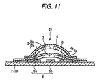
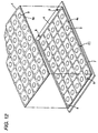
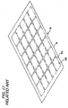
- Fig. 14 is a view showing a panel switch 21 manufactured when the upper and the lower insulating film 4 having the moving contacts 3 are put on each other, and the excess film has been removed.
- a separator 2B it is possible to use a separator 2B in place of the wiring board 2.
- a laser beam is simultaneously irradiated onto the plurality of insulating films and an excess portion is cut off. Therefore, no shift is caused in the sticking operation.
- two insulating films which have been formed in the moving contact sticking operation, are put on each other and arranged on the wiring board or the separator. Accordingly, on the two respective insulating films, a setting adjustment of adjusting an operation load (i.e., a switch pushing load) of the moving contact can be executed independently from each other.
- an operation load i.e., a switch pushing load
- production can be executed without using a metallic die. Therefore, it is possible to eliminate the cost of manufacturing the metallic die and it is also possible to shorten a period of time of manufacturing the panel switch.
- the plurality of insulating films in a case in which a plurality of insulating films are put on each other, the plurality of insulating films can be simultaneously and accurately cut by irradiating a laser beam. Accordingly, no positional shift is caused between the plurality of insulating films, and a yield of manufacturing the panel switches can be increased. Further, it is possible to reduce a pitch between the plurality of moving contacts. Accordingly, an area of the excess portion of the insulating film can be reduced and made smaller than that of the related art panel switch.
- the operation load can be set in a wide range with high accuracy and a "click" feeling at the time of operating the switch can be enhanced over that of the related art panel switch.
Landscapes
- Push-Button Switches (AREA)
- Manufacture Of Switches (AREA)
- Laser Beam Processing (AREA)
Applications Claiming Priority (1)
| Application Number | Priority Date | Filing Date | Title |
|---|---|---|---|
| JP2007171120A JP4442648B2 (ja) | 2007-06-28 | 2007-06-28 | パネルスイッチの製造方法及びパネルスイッチ |
Publications (3)
| Publication Number | Publication Date |
|---|---|
| EP2009660A2 true EP2009660A2 (de) | 2008-12-31 |
| EP2009660A3 EP2009660A3 (de) | 2010-06-09 |
| EP2009660B1 EP2009660B1 (de) | 2012-04-18 |
Family
ID=39789646
Family Applications (1)
| Application Number | Title | Priority Date | Filing Date |
|---|---|---|---|
| EP08011590A Expired - Fee Related EP2009660B1 (de) | 2007-06-28 | 2008-06-26 | Verfahren zum Herstellen eines Tafelschalters und Tafelschalter |
Country Status (5)
| Country | Link |
|---|---|
| US (1) | US8091212B2 (de) |
| EP (1) | EP2009660B1 (de) |
| JP (1) | JP4442648B2 (de) |
| CN (1) | CN101335147B (de) |
| TW (1) | TW200901250A (de) |
Cited By (10)
| Publication number | Priority date | Publication date | Assignee | Title |
|---|---|---|---|---|
| EP2849861A4 (de) * | 2012-05-15 | 2016-04-13 | Microsoft Technology Licensing Llc | Herstellung einer eingabevorrichtung |
| US9618977B2 (en) | 2012-03-02 | 2017-04-11 | Microsoft Technology Licensing, Llc | Input device securing techniques |
| US9661770B2 (en) | 2012-10-17 | 2017-05-23 | Microsoft Technology Licensing, Llc | Graphic formation via material ablation |
| US9678542B2 (en) | 2012-03-02 | 2017-06-13 | Microsoft Technology Licensing, Llc | Multiple position input device cover |
| US9706089B2 (en) | 2012-03-02 | 2017-07-11 | Microsoft Technology Licensing, Llc | Shifted lens camera for mobile computing devices |
| US9793073B2 (en) | 2012-03-02 | 2017-10-17 | Microsoft Technology Licensing, Llc | Backlighting a fabric enclosure of a flexible cover |
| US9870066B2 (en) | 2012-03-02 | 2018-01-16 | Microsoft Technology Licensing, Llc | Method of manufacturing an input device |
| US9959241B2 (en) | 2012-05-14 | 2018-05-01 | Microsoft Technology Licensing, Llc | System and method for accessory device architecture that passes via intermediate processor a descriptor when processing in a low power state |
| US10031556B2 (en) | 2012-06-08 | 2018-07-24 | Microsoft Technology Licensing, Llc | User experience adaptation |
| USRE48963E1 (en) | 2012-03-02 | 2022-03-08 | Microsoft Technology Licensing, Llc | Connection device for computing devices |
Families Citing this family (8)
| Publication number | Priority date | Publication date | Assignee | Title |
|---|---|---|---|---|
| CN101972917A (zh) * | 2010-09-29 | 2011-02-16 | 常州市德春电器有限公司 | 高压开关外转盘加工工艺 |
| KR101153993B1 (ko) * | 2011-08-09 | 2012-06-11 | 주식회사 두성테크 | 테이프 시트 연배열 부착 방법 |
| US9426905B2 (en) | 2012-03-02 | 2016-08-23 | Microsoft Technology Licensing, Llc | Connection device for computing devices |
| JP6035889B2 (ja) * | 2012-06-14 | 2016-11-30 | 大日本印刷株式会社 | 電子部品内蔵カード、アッセンブリ |
| JP6107039B2 (ja) * | 2012-10-04 | 2017-04-05 | ミツミ電機株式会社 | スイッチの製造方法 |
| US8654030B1 (en) | 2012-10-16 | 2014-02-18 | Microsoft Corporation | Antenna placement |
| US20140159758A1 (en) * | 2012-12-12 | 2014-06-12 | Qualcomm Incorporated | Assembly for optical backside failure analysis of package-on-package (pop) during electrical testing |
| CN111312786B (zh) * | 2020-02-28 | 2022-11-15 | 云谷(固安)科技有限公司 | 柔性显示面板及其制备方法 |
Citations (2)
| Publication number | Priority date | Publication date | Assignee | Title |
|---|---|---|---|---|
| JP2003100165A (ja) | 2001-09-19 | 2003-04-04 | Matsushita Electric Ind Co Ltd | 可動接点体とその製造方法、及びこの可動接点体を用いたパネルスイッチの製造方法 |
| JP2007171120A (ja) | 2005-12-26 | 2007-07-05 | Ntn Corp | 鋼材測定コイル |
Family Cites Families (12)
| Publication number | Priority date | Publication date | Assignee | Title |
|---|---|---|---|---|
| US5071088A (en) * | 1989-11-29 | 1991-12-10 | The United States Of America As Represented By The Secretary Of The Navy | High lift aircraft |
| JP3988203B2 (ja) * | 1996-10-22 | 2007-10-10 | 松下電器産業株式会社 | パネルスイッチ用可動接点体 |
| TW388894B (en) | 1997-10-09 | 2000-05-01 | Nissha Printing | High strength touch panel and manufacturing method therefor |
| JP2002008485A (ja) | 2000-06-19 | 2002-01-11 | Matsushita Electric Ind Co Ltd | キー操作装置 |
| JP2002082772A (ja) | 2000-06-28 | 2002-03-22 | Hitachi Ltd | タッチパネルとその製造方法および、このタッチパネルを用いた画面入力型表示装置 |
| JP2003151393A (ja) | 2001-11-15 | 2003-05-23 | Matsushita Electric Ind Co Ltd | 可動接点体およびそれを用いたパネルスイッチ、並びにそのパネルスイッチを装着した電子機器 |
| JP2005216799A (ja) | 2004-02-02 | 2005-08-11 | Matsushita Electric Ind Co Ltd | 可動接点体 |
| US7301114B2 (en) | 2004-02-02 | 2007-11-27 | Matsushita Electric Industrial Co., Ltd. | Movable contact unit |
| JP2005259460A (ja) | 2004-03-10 | 2005-09-22 | Alps Electric Co Ltd | 可動接点付シート及びこれを用いた入力装置 |
| JP4607477B2 (ja) | 2004-03-12 | 2011-01-05 | 日本碍子株式会社 | フィルム貼り加工機 |
| US20050271442A1 (en) | 2004-06-02 | 2005-12-08 | Inventec Appliances Corporation | High voltage resisting keyboard |
| JP4878957B2 (ja) | 2005-10-18 | 2012-02-15 | アルプス電気株式会社 | 粘着シートの製造方法及び粘着シート |
-
2007
- 2007-06-28 JP JP2007171120A patent/JP4442648B2/ja active Active
-
2008
- 2008-01-08 CN CN2008100017473A patent/CN101335147B/zh active Active
- 2008-01-10 TW TW097101067A patent/TW200901250A/zh unknown
- 2008-06-26 US US12/147,013 patent/US8091212B2/en not_active Expired - Fee Related
- 2008-06-26 EP EP08011590A patent/EP2009660B1/de not_active Expired - Fee Related
Patent Citations (2)
| Publication number | Priority date | Publication date | Assignee | Title |
|---|---|---|---|---|
| JP2003100165A (ja) | 2001-09-19 | 2003-04-04 | Matsushita Electric Ind Co Ltd | 可動接点体とその製造方法、及びこの可動接点体を用いたパネルスイッチの製造方法 |
| JP2007171120A (ja) | 2005-12-26 | 2007-07-05 | Ntn Corp | 鋼材測定コイル |
Cited By (18)
| Publication number | Priority date | Publication date | Assignee | Title |
|---|---|---|---|---|
| US9793073B2 (en) | 2012-03-02 | 2017-10-17 | Microsoft Technology Licensing, Llc | Backlighting a fabric enclosure of a flexible cover |
| US9870066B2 (en) | 2012-03-02 | 2018-01-16 | Microsoft Technology Licensing, Llc | Method of manufacturing an input device |
| US9619071B2 (en) | 2012-03-02 | 2017-04-11 | Microsoft Technology Licensing, Llc | Computing device and an apparatus having sensors configured for measuring spatial information indicative of a position of the computing devices |
| USRE48963E1 (en) | 2012-03-02 | 2022-03-08 | Microsoft Technology Licensing, Llc | Connection device for computing devices |
| US9678542B2 (en) | 2012-03-02 | 2017-06-13 | Microsoft Technology Licensing, Llc | Multiple position input device cover |
| US9706089B2 (en) | 2012-03-02 | 2017-07-11 | Microsoft Technology Licensing, Llc | Shifted lens camera for mobile computing devices |
| US9710093B2 (en) | 2012-03-02 | 2017-07-18 | Microsoft Technology Licensing, Llc | Pressure sensitive key normalization |
| US9766663B2 (en) | 2012-03-02 | 2017-09-19 | Microsoft Technology Licensing, Llc | Hinge for component attachment |
| US9618977B2 (en) | 2012-03-02 | 2017-04-11 | Microsoft Technology Licensing, Llc | Input device securing techniques |
| US10963087B2 (en) | 2012-03-02 | 2021-03-30 | Microsoft Technology Licensing, Llc | Pressure sensitive keys |
| US9852855B2 (en) | 2012-03-02 | 2017-12-26 | Microsoft Technology Licensing, Llc | Pressure sensitive key normalization |
| US9904327B2 (en) | 2012-03-02 | 2018-02-27 | Microsoft Technology Licensing, Llc | Flexible hinge and removable attachment |
| US9946307B2 (en) | 2012-03-02 | 2018-04-17 | Microsoft Technology Licensing, Llc | Classifying the intent of user input |
| US10013030B2 (en) | 2012-03-02 | 2018-07-03 | Microsoft Technology Licensing, Llc | Multiple position input device cover |
| US9959241B2 (en) | 2012-05-14 | 2018-05-01 | Microsoft Technology Licensing, Llc | System and method for accessory device architecture that passes via intermediate processor a descriptor when processing in a low power state |
| EP2849861A4 (de) * | 2012-05-15 | 2016-04-13 | Microsoft Technology Licensing Llc | Herstellung einer eingabevorrichtung |
| US10031556B2 (en) | 2012-06-08 | 2018-07-24 | Microsoft Technology Licensing, Llc | User experience adaptation |
| US9661770B2 (en) | 2012-10-17 | 2017-05-23 | Microsoft Technology Licensing, Llc | Graphic formation via material ablation |
Also Published As
| Publication number | Publication date |
|---|---|
| JP2009009854A (ja) | 2009-01-15 |
| TW200901250A (en) | 2009-01-01 |
| US20090000934A1 (en) | 2009-01-01 |
| CN101335147A (zh) | 2008-12-31 |
| EP2009660B1 (de) | 2012-04-18 |
| US8091212B2 (en) | 2012-01-10 |
| CN101335147B (zh) | 2012-05-09 |
| EP2009660A3 (de) | 2010-06-09 |
| JP4442648B2 (ja) | 2010-03-31 |
Similar Documents
| Publication | Publication Date | Title |
|---|---|---|
| US8091212B2 (en) | Method of manufacturing panel switch | |
| US11282659B2 (en) | Singulated keyboard assemblies and methods for assembling a keyboard | |
| US10741344B2 (en) | Keyboard for electronic device | |
| US7166813B2 (en) | Multistep switch having capacitive type sensor | |
| US20120055773A1 (en) | Push switch and method for manufacturing the same | |
| WO2005096683A1 (ja) | 回路基板及びその製造方法及び回路基板を用いたジョイントボックス | |
| DE102008014033A1 (de) | Eingabevorrichtung und Verfahren zum Herstellen derselben | |
| EP1329919B1 (de) | Tastschalter, Tastatur und ein elektronisches Gerät mit einem solchen Tastschalter | |
| EP1524679B1 (de) | Beweglicher Kontakt für einen Tastschalter und Tastschalter | |
| KR101942960B1 (ko) | 돔 시트 및 돔 스위치 제조방법 | |
| US8089018B2 (en) | Movable contact unit and method of manufacturing the same | |
| US20040154912A1 (en) | Movable contact unit with operating projections, method of mounting operating projections and operating panel switch using movable contact unit with operating projections | |
| US6073341A (en) | Dome switch assembly system | |
| US20060159506A1 (en) | Keypad module manufacturing method | |
| US6483051B2 (en) | Method in the manufacture of a keyboard for an electronic device | |
| US6634090B2 (en) | Method of production of series of a tactile contact units and tactile contact unit, and series of tactile contact units and a tactile contact unit produced by using the same method | |
| JP2010097708A (ja) | キースイッチ及びスイッチシート | |
| CN223528282U (zh) | 一种fpc冲切成型结构 | |
| JPH10255589A (ja) | プッシュスイッチおよびその製造方法 | |
| CN109429425A (zh) | 柔性印刷电路板的制造方法、制造治具以及制造装置 | |
| JP2003100165A (ja) | 可動接点体とその製造方法、及びこの可動接点体を用いたパネルスイッチの製造方法 | |
| JP2001328094A (ja) | 原基板分割装置 | |
| JP2022065891A (ja) | キースイッチ |
Legal Events
| Date | Code | Title | Description |
|---|---|---|---|
| PUAI | Public reference made under article 153(3) epc to a published international application that has entered the european phase |
Free format text: ORIGINAL CODE: 0009012 |
|
| AK | Designated contracting states |
Kind code of ref document: A2 Designated state(s): AT BE BG CH CY CZ DE DK EE ES FI FR GB GR HR HU IE IS IT LI LT LU LV MC MT NL NO PL PT RO SE SI SK TR |
|
| AX | Request for extension of the european patent |
Extension state: AL BA MK RS |
|
| PUAL | Search report despatched |
Free format text: ORIGINAL CODE: 0009013 |
|
| AK | Designated contracting states |
Kind code of ref document: A3 Designated state(s): AT BE BG CH CY CZ DE DK EE ES FI FR GB GR HR HU IE IS IT LI LT LU LV MC MT NL NO PL PT RO SE SI SK TR |
|
| AX | Request for extension of the european patent |
Extension state: AL BA MK RS |
|
| 17P | Request for examination filed |
Effective date: 20101208 |
|
| AKX | Designation fees paid |
Designated state(s): DE FR GB |
|
| 17Q | First examination report despatched |
Effective date: 20110119 |
|
| RIC1 | Information provided on ipc code assigned before grant |
Ipc: H01H 13/88 20060101ALI20110606BHEP Ipc: H01H 13/48 20060101AFI20110606BHEP |
|
| GRAP | Despatch of communication of intention to grant a patent |
Free format text: ORIGINAL CODE: EPIDOSNIGR1 |
|
| GRAS | Grant fee paid |
Free format text: ORIGINAL CODE: EPIDOSNIGR3 |
|
| GRAA | (expected) grant |
Free format text: ORIGINAL CODE: 0009210 |
|
| AK | Designated contracting states |
Kind code of ref document: B1 Designated state(s): DE FR GB |
|
| REG | Reference to a national code |
Ref country code: GB Ref legal event code: FG4D |
|
| REG | Reference to a national code |
Ref country code: DE Ref legal event code: R096 Ref document number: 602008014848 Country of ref document: DE Effective date: 20120614 |
|
| PGFP | Annual fee paid to national office [announced via postgrant information from national office to epo] |
Ref country code: DE Payment date: 20120627 Year of fee payment: 5 |
|
| PGFP | Annual fee paid to national office [announced via postgrant information from national office to epo] |
Ref country code: GB Payment date: 20120529 Year of fee payment: 5 Ref country code: FR Payment date: 20120608 Year of fee payment: 5 |
|
| PLBE | No opposition filed within time limit |
Free format text: ORIGINAL CODE: 0009261 |
|
| STAA | Information on the status of an ep patent application or granted ep patent |
Free format text: STATUS: NO OPPOSITION FILED WITHIN TIME LIMIT |
|
| 26N | No opposition filed |
Effective date: 20130121 |
|
| REG | Reference to a national code |
Ref country code: DE Ref legal event code: R097 Ref document number: 602008014848 Country of ref document: DE Effective date: 20130121 |
|
| GBPC | Gb: european patent ceased through non-payment of renewal fee |
Effective date: 20130626 |
|
| REG | Reference to a national code |
Ref country code: DE Ref legal event code: R119 Ref document number: 602008014848 Country of ref document: DE Effective date: 20140101 |
|
| REG | Reference to a national code |
Ref country code: FR Ref legal event code: ST Effective date: 20140228 |
|
| PG25 | Lapsed in a contracting state [announced via postgrant information from national office to epo] |
Ref country code: DE Free format text: LAPSE BECAUSE OF NON-PAYMENT OF DUE FEES Effective date: 20140101 Ref country code: GB Free format text: LAPSE BECAUSE OF NON-PAYMENT OF DUE FEES Effective date: 20130626 |
|
| PG25 | Lapsed in a contracting state [announced via postgrant information from national office to epo] |
Ref country code: FR Free format text: LAPSE BECAUSE OF NON-PAYMENT OF DUE FEES Effective date: 20130701 |