EP2009692A1 - Elektronisches Modul und Herstellungsverfahren dafür - Google Patents
Elektronisches Modul und Herstellungsverfahren dafür Download PDFInfo
- Publication number
- EP2009692A1 EP2009692A1 EP08011741A EP08011741A EP2009692A1 EP 2009692 A1 EP2009692 A1 EP 2009692A1 EP 08011741 A EP08011741 A EP 08011741A EP 08011741 A EP08011741 A EP 08011741A EP 2009692 A1 EP2009692 A1 EP 2009692A1
- Authority
- EP
- European Patent Office
- Prior art keywords
- ground electrode
- insulating layer
- electronic
- cutting
- electronic module
- Prior art date
- Legal status (The legal status is an assumption and is not a legal conclusion. Google has not performed a legal analysis and makes no representation as to the accuracy of the status listed.)
- Withdrawn
Links
Images









Classifications
-
- H—ELECTRICITY
- H10—SEMICONDUCTOR DEVICES; ELECTRIC SOLID-STATE DEVICES NOT OTHERWISE PROVIDED FOR
- H10W—GENERIC PACKAGES, INTERCONNECTIONS, CONNECTORS OR OTHER CONSTRUCTIONAL DETAILS OF DEVICES COVERED BY CLASS H10
- H10W42/00—Arrangements for protection of devices
- H10W42/20—Arrangements for protection of devices protecting against electromagnetic or particle radiation, e.g. light, X-rays, gamma-rays or electrons
-
- H—ELECTRICITY
- H10—SEMICONDUCTOR DEVICES; ELECTRIC SOLID-STATE DEVICES NOT OTHERWISE PROVIDED FOR
- H10W—GENERIC PACKAGES, INTERCONNECTIONS, CONNECTORS OR OTHER CONSTRUCTIONAL DETAILS OF DEVICES COVERED BY CLASS H10
- H10W42/00—Arrangements for protection of devices
- H10W42/20—Arrangements for protection of devices protecting against electromagnetic or particle radiation, e.g. light, X-rays, gamma-rays or electrons
- H10W42/261—Arrangements for protection of devices protecting against electromagnetic or particle radiation, e.g. light, X-rays, gamma-rays or electrons characterised by their shapes or dispositions
- H10W42/276—Arrangements for protection of devices protecting against electromagnetic or particle radiation, e.g. light, X-rays, gamma-rays or electrons characterised by their shapes or dispositions the arrangements being on an external surface of the package, e.g. on the outer surface of an encapsulation
-
- H—ELECTRICITY
- H10—SEMICONDUCTOR DEVICES; ELECTRIC SOLID-STATE DEVICES NOT OTHERWISE PROVIDED FOR
- H10W—GENERIC PACKAGES, INTERCONNECTIONS, CONNECTORS OR OTHER CONSTRUCTIONAL DETAILS OF DEVICES COVERED BY CLASS H10
- H10W72/00—Interconnections or connectors in packages
- H10W72/01—Manufacture or treatment
- H10W72/0198—Manufacture or treatment batch processes
-
- H—ELECTRICITY
- H10—SEMICONDUCTOR DEVICES; ELECTRIC SOLID-STATE DEVICES NOT OTHERWISE PROVIDED FOR
- H10W—GENERIC PACKAGES, INTERCONNECTIONS, CONNECTORS OR OTHER CONSTRUCTIONAL DETAILS OF DEVICES COVERED BY CLASS H10
- H10W70/00—Package substrates; Interposers; Redistribution layers [RDL]
- H10W70/60—Insulating or insulated package substrates; Interposers; Redistribution layers
-
- H—ELECTRICITY
- H10—SEMICONDUCTOR DEVICES; ELECTRIC SOLID-STATE DEVICES NOT OTHERWISE PROVIDED FOR
- H10W—GENERIC PACKAGES, INTERCONNECTIONS, CONNECTORS OR OTHER CONSTRUCTIONAL DETAILS OF DEVICES COVERED BY CLASS H10
- H10W74/00—Encapsulations, e.g. protective coatings
-
- Y—GENERAL TAGGING OF NEW TECHNOLOGICAL DEVELOPMENTS; GENERAL TAGGING OF CROSS-SECTIONAL TECHNOLOGIES SPANNING OVER SEVERAL SECTIONS OF THE IPC; TECHNICAL SUBJECTS COVERED BY FORMER USPC CROSS-REFERENCE ART COLLECTIONS [XRACs] AND DIGESTS
- Y10—TECHNICAL SUBJECTS COVERED BY FORMER USPC
- Y10T—TECHNICAL SUBJECTS COVERED BY FORMER US CLASSIFICATION
- Y10T29/00—Metal working
- Y10T29/49—Method of mechanical manufacture
- Y10T29/49002—Electrical device making
- Y10T29/49117—Conductor or circuit manufacturing
Definitions
- the present invention relates to an electronic module and fabrication method thereof.
- FIG. 11 is a perspective view illustrating the main section of a prior art electronic module 200; and FIG. 12 is a cross-sectional view of the electronic module 200 taken along the line XII-XII.
- the electronic module 200 includes: a circuit substrate 210 having an electronic component 220 mounted on at least one surface thereof; a sealing layer 225 composed of epoxy resin or the like covering the electronic component 220; and a metal shield 230 arranged to cover the sealing layer 225.
- the metal shield 230 plays a role of blocking electromagnetic wave from the outside to stabilize circuit characteristics and at' the same time, prevents electromagnetic wave radiated from the electronic component 220 from leaking to the outside, thereby allowing the electronic component 220 to operate normally.
- FIG. 13 is a top view of the circuit substrate 210 before the sealing layer 225 and metal shield 230 are formed. As illustrated in FIG. 13 , in the peripheral edge on the circuit substrate 210, there is formed a ground electrode 221. After this circuit substrate 210 is covered with the sealing layer 225 composed of epoxy resin or the like, the section of the sealing layer 225 over the ground electrode 221 is cut away using a cutoff blade or cutting blade (not illustrated) such as a dicing blade, so that the ground electrode 221 is exposed.
- a cutoff blade or cutting blade such as a dicing blade
- the metal shield 230 is formed by plating or the like on the sealing layer 225 and the exposed ground electrode 221, whereby the ground electrode 221 and metal shield 230 are electrically and mechanically connected (for example, refer to Japanese Patent Laid-Open No. 2004-193187 ).
- the prior art electronic module 200 since the ground electrode 221 lies on the surface of the circuit substrate 210, the peripheral edge area of the circuit substrate 210 is occupied by the ground electrode 221 and thus the mounting area of the electronic component 220 on the circuit substrate 210 is limited. Further, since the prior art electronic module 200 is designed from a viewpoint of ensuring the mounting area of the electronic component 220, it is difficult to set a sufficiently large exposed area of the ground electrode 221 to enhance the connection reliability and connection strength between the metal shield 230 and ground electrode 221, so the electrical and mechanical connection strength between the ground electrode 221 and metal shield 230 may be insufficient.
- the actual cutting position by the cutoff blade may be dislocated from the target position due to misalignment and the like of the circuit substrate 210; as a result, the intended ground electrode 221 may not be exposed, resulting in connection failure between the ground electrode 221 and metal shield 230.
- the present invention has been devised in view of the above circumstances and has an object to provide an electronic module and fabrication method thereof in which the mounting area of an electronic component can be increased, while the connection strength between a ground electrode and conductive shield can be sufficiently ensured and it is also possible to suppress connection failure between the ground electrode and metal shield even when a cutting position misalignment occurs.
- an electronic module includes: an insulating layer; a ground electrode arranged in the insulating layer and partly exposed from a side surface of the insulating layer; an electronic component mounted on the insulating layer; and a sealing layer which seals the electronic component; a conductive shield which covers the sealing layer and is electrically connected to the ground electrode at an exposed section of the ground electrode.
- the electronic component mounted on the insulating layer is sealed by the sealing layer; the resultant structure is wholly covered with the conductive shield; the conductive shield is electrically connected to the ground electrode partly exposed from the insulating layer; and the ground electrode is usually connected to a ground potential such as housing ground.
- the electronic component is electromagnetically shielded from the outside.
- a part of the ground electrode is exposed from a side surface of the insulating layer and connected to the conductive shield at the exposed section; consequently, the peripheral edge area, needed in the prior art electronic module, for mounting the ground electrode on the substrate surface is reduced.
- the ground electrode and conductive shield are connected at an outer edge on the lower side of the electronic component mounting area, so a connection area between the two parts does not need to be specially provided.
- the insulating layer may simply be drilled or cut in a depth direction.
- a part of the ground electrode is more correctly exposed, compared to the prior art in which the level in a depth direction is adjusted and the sealing layer is removed to expose the surface of the ground electrode. Consequently, non-exposure of the ground electrode caused by a cutting misalignment which may occur in the prior art electronic module is reliably eliminated, thus ensuring the connection with the conductive shield and also preventing the connection failure between the two parts.
- a ground electrode is usually arranged in the insulating layer of the substrate module.
- the existing ground electrode arranged in the substrate module can also serve as the ground electrode of the electronic module. Consequently, there is no need to form an additional ground electrode used to shield the electronic module, so the number of processes and constituent components is reduced, significantly improving productivity.
- a plurality of the ground electrodes having the exposed section are preferably provided in a direction perpendicular to the insulating layer.
- the exposed area of the ground electrode in the side surface of the insulating layer is enlarged, so the connection strength with the conductive shield can be further increased.
- the side surface of the exposed section of the ground electrode in the side surface of the insulating layer preferably has a prescribed inclination (taper) relative to a direction perpendicular to the insulating layer (a direction perpendicular to the insulating layer plane: normal line direction).
- the bottom end of the insulating layer is preferably positioned at an inner side relative to the end face of the conductive shield.
- the insulating layer can be prevented from protruding to the outside relative to the conductive shield, so that the substantial effective area of the substrate can be enlarged, allowing downsizing of the module.
- an electronic module fabrication method for fabricating a plurality of electronic modules including electronic components including the steps of: forming an insulating layer having a ground electrode; mounting on the insulating layer, a plurality of electronic components included in the plurality of electronic modules; forming on the insulating layer and the plurality of electronic components, a sealing layer which seals the plurality of electronic components; cutting the insulating layer and the sealing layer so as to expose a part of the ground electrode from a side surface of the insulating layer; and forming a conductive shield which covers the sealing layer and is electrically connected to the ground electrode at an exposed section of the ground electrode.
- the step of forming the insulating layer having the ground electrode includes forming the insulating layer in which the ground electrode extends across at least two areas of the areas where the electronic modules are formed; and the step of cutting the insulating layer and sealing layer includes cutting the insulating layer and sealing layer so as to define each of the areas where the electronic modules are formed and to.expose a part of the ground electrode from the side surface of the insulating layer.
- the ground electrode extends across at least two areas of the areas where the electronic modules.are formed, a plurality of the electronic components included in the plurality of electronic modules are mounted and the resultant structure is wholly sealed by the sealing layer, and thereafter the insulating layer is cut so as to define each of the electronic modules, the ground electrode is divided and exposed, and the conductive shield is formed across a plurality of the electronic modules to complete the shield all at once and then separation is carried out, so productivity can be improved.
- the distance between the electronic modules can be shortened and thus the arrangement density of electronic modules in a common substrate is enhanced, further improving productivity.
- a plurality of the ground electrodes are preferably formed in a direction perpendicular to the insulating layer; and in cutting the insulating layer and sealing layer, the cutting is preferably carried out so that a plurality of the ground electrodes are preferably exposed from the side surface of the insulating layer.
- the cutting is preferably carried out so that a plurality of the ground electrodes are preferably exposed from the side surface of the insulating layer.
- the cutting is preferably carried out so that the exposed section of the ground electrode on the side surface of the insulating layer has a prescribed inclination (taper) relative to a direction perpendicular to the insulating layer. More specifically, for example, there may be performed dicing in which the tip end of a cutting blade having a spire-shaped (tapered) tip end side wall reaches the buried section of the ground electrode in the insulating layer.
- the cutoff is preferably performed by making an incision from a surface opposite to the cut surface to the cut position; and in performing the cutoff by making an incision, the incision is preferably made so that the bottom end of the insulating layer is positioned at an inner side relative to the end face of the conductive shield.
- the cutoff portion can be prevented from protruding to the outside relative to the conductive shield, so that the substantial effective area of the substrate can be enlarged, allowing downsizing of the module.
- the incision is preferably made using a cutoff blade having a blade thickness larger than that of the cutoff blade used for the cutting.
- the conductive shield used to shield the electronic components is connected with the ground electrode exposed on the side surface of the insulating layer; thus the ground electrode arranged in the peripheral edge of substrate and its formation area according to the prior art can be reduced to enlarge the mounting area of the electronic components, allowing further downsizing by higher mounting density; further the ground electrode and conductive shield can be reliably connected and in addition, connection failure caused by non-exposure of the ground electrode can be prevented, allowing improvement in product reliability, yield rate and productivity.
- FIG. 1 is a schematic cross-sectional view illustrating the main section of an electronic module according to the present embodiment.
- An electronic module 100 includes; a multi-layer substrate 1 having mounted thereon an electronic component 60 and also incorporating a semiconductor device 30 and the like; a sealing layer 110 which seals the electronic component 60 mounted on the multi-layer substrate 1, using epoxy resin or the like; and a metal shield 120 which covers the sealing layer 110 and multi-layer substrate 1.
- the multi-layer substrate 1 and metal shield 120 are electrically connected via a ground electrode GN exposed by cutting away a part of the multi-layer substrate 1.
- a resin layer 41 is formed on one surface (the illustrated lower surface) of a base 10; and the semiconductor device 30 is buried in the interior of the resin layer 41.
- the "resin layer” according to the present invention is constituted of the resin layers 41, 42 and 43.
- materials used for the resin layers (insulating layers) 41, 42 and 43 include simple resins such as vinyl benzyl resin, polyvinyl benzyl ether compound resin, bismaleimide triazine resin (BT resin), polyphenylene ether (polyphenylene ether oxide) resin (PPE, PPO), cyanate ester resin, epoxy + active ester curable resin, polyphenylene ether resin (polyphenylene oxide resin), curable polyolefin resin, benzocyclobutene resin, polyimide resin, aromatic polyester resin, aromatic liquid crystal polyester resin, polyphenylene sulfide resin, polyetherimide resin, polyacrylate resin, polyether ether ketone resin, fluorine resin, epoxy resin, phenol resin and benzoxazine resin; materials obtained by adding, to these resins, silica, talc, calcium carbonate, magnesium carbonate, aluminum hydroxide, magnesium hydroxide, aluminum borate whisker, potassium titanate fibers, alumina, glass flakes, glass phosphat
- FIG. 2 is a perspective view schematically illustrating the structure of the semiconductor device 30.
- the semiconductor device 30 is a bare chip semiconductor IC (die) or the like, and has many land electrodes 31 arranged on a primary surface 30a having a substantially rectangular board shape.
- the land electrode 31 and a bump 32 to be described later are illustrated only in the four corners; illustration of the land electrode 31 is omitted except the above ones.
- the type of the semiconductor device 30 is not particularly limited, but examples thereof include a digital IC having a significantly high operating frequency such as CPU and DSP.
- the rear surface 30b of the semiconductor device 30 is polished so that thickness t (the distance from the primary surface 30a to the rear surface 30b) of the semiconductor device 30 is smaller than that of the typical semiconductor IC, and preferably equal to or smaller than 200 ⁇ m, and more preferably 20 to 50 ⁇ m.
- roughening processing by etching, plasma processing, laser processing, blasting, buffing, chemical treatment or the like is preferably applied to the rear surface 30b.
- the polishing of the rear surface 30b of the semiconductor device 30 can be performed after separation into the individual semiconductor devices 30 has been performed by dicing.
- many electronic components may be polished collectively in the wafer state and may be subsequently separated into the individual semiconductor devices 30 by dicing.
- an alternative method is such that many electronic components is polished all at once in the wafer state and then separation into the individual semiconductor devices 30 is performed by dicing and thereafter the individual electronic components are polished to further slim down the semiconductor devices 30.
- a bump (terminal) 32 that is a type of a conductive protrusion is formed on each land electrode 31.
- the type of the bump 32 is not particularly limited, and examples of the bump 32 include stud bump, plate bump, plating bump and ball bump.
- a stud bump is illustrated.
- the bump can be formed by wire bonding using silver (Ag) or copper (Cu); when a plate bump is used, the bump can be formed by plating, sputtering or deposition.
- the bumps may be formed by plating, and when ball bumps are used, the bumps may be formed by either mounting a solder ball on the land electrode 31 and then melting the same or by printing a cream solder on the land electrode and then melting the same. Also usable are bumps having a conical shape, a cylindrical shape or the like formed by screen-printing and curing a conductive paste, or bumps formed by printing a metal paste and sintering the same by heating.
- the type of metal used for the bump 32 is not particularly limited, and examples thereof include gold (Au), silver (Ag), copper (Cu), nickel (Ni), tin (Sn), chrome (Cr), nickel-chrome alloy and solder. Among these, copper is preferably used. When copper is used for the bump 32, a high-strength bond to the land electrode 31 can be achieved, compared to a case where gold is used, and thus the reliability of the semiconductor device 30 itself can be enhanced.
- the dimensions and shape of the bump 32 can be properly set according to the interval (pitch) between the land electrodes 31. For example, when the pitch of the land electrode 31 is about 100 ⁇ m, the maximum diameter of the bump 32 is 10 to 90 ⁇ m and the height , thereof, 2 to 100 ⁇ m.
- the bump 32 can be joined to each of the land electrodes 31 by use of a wire bonder after the wafer has been cut off and separated into individual semiconductor devices 30 by dicing.
- each of the bumps 32 is arranged in the interior of the resin layer 41 while connected to the wire 51 at the connection section 13 ( FIG. 1 ).
- cutting reference line S used for division into the electronic modules 100 is indicated by the dashed-dotted line.
- FIG. 7 is a plan view illustrating an exemplary relationship between the ground electrode GN and cutting reference line S formed in the wire 51, wire 52 and the like.
- electrode width W0 of the ground electrode GN formed in the wire 51, wire 52 and the like is set larger than the wire width, and according to the present embodiment, the ground electrode GN is formed so as to extend across the wires 51 and 52 of the adjoining multi-layer substrates 1.
- the integrated multi-layer substrate 1a including the ground electrode GN extending across the adjoining multi-layer substrates 1.
- the ground electrode GN When the ground electrode GN is formed in this way, even when the actual cutting position is dislocated from the cutting reference line S, if the misalignment falls into the electrode width W0 of the ground electrode GN, the ground electrode GN can be correctly exposed. Accordingly, in contrast to the prior art in which the level in a depth direction is adjusted and the sealing layer is removed to expose the.surface of the ground electrode, a part of the ground electrode is correctly exposed. Thus, non-exposure of the ground electrode caused by a cutting misalignment which may occur in the prior art electronic module is reliably eliminated, thus ensuring the connection with the conductive shield and preventing the connection failure between the two parts.
- the sealing layer 110 composed of epoxy resin is formed so as to cover the electronic component 60 mounted on the surface of the integrated multi-layer substrate 1a.
- the sealing layer 110 contains epoxy resin of 1 to 500 Pa.s, filler having an average particle diameter less than 100 ⁇ m, and curing agent, for example.
- An inorganic material such as silica and aluminum hydroxide is used for the filler.
- a curing agent such as anhydride and amine family is selected according to the mechanical characteristics of the electronic component 60 and used for the sealing layer 110.
- the sealing layer 110 composed of epoxy resin is supplied around the electronic component 60 by use of a fixing frame and squeegee (not illustrated) and thereafter defoaming is performed using a vacuum chamber. More specifically, the vacuum of the vacuum chamber is set equal to or lower than 1.0 x 10 2 Pa to allow defoaming. Here, in order to further remove bubbles contained in the epoxy resin, before supplying epoxy resin, the vacuum of the vacuum chamber is adjusted equal to or lower than 1.0 x 10 2 Pa, and then epoxy resin is supplied.
- the vacuum of the vacuum chamber is set equal to or more than 1.0 x 10 4 Pa.
- the vacuum is lowered in this way, bubbles in the paste can be removed by the pressure difference from the initial state.
- the sealing layer After the supplying of epoxy resin and defoaming, the sealing layer is placed in an oven at a degree of 100°C for an hour, and further placed in an oven at a degree of 150°C for three hours to cure the sealing layer 110 composed of epoxy resin.
- the curing of the sealing layer 110 is gradually performed in two stages, so that the difference of thermal expansion coefficient between the sealing layer 110 and integrated multi-layer substrate 1a and the internal stress caused by curing and contraction of the sealing layer 110 are decreased.
- warpage of the integrated multi-layer substrate 1a can be reduced to improve the reliability of thermal cycle and the like.
- the sealing layer 110 is cooled at a degree equal to or lower than 0.5°C/minute. In this way, when the temperature is gradually'lowered, warpage of the integrated multi-layer substrate 1a can be further reduced.
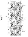
- the ground electrode GN is exposed by cutting the sealing layer 110 and integrated multi-layer substrate 1a by use of a dicing blade or the like along the cutting reference line S so that a V-shaped cross section (refer to inclination angle ⁇ illustrated in FIG. 5 ) is formed.
- a V-shaped cross section (refer to inclination angle ⁇ illustrated in FIG. 5 ) is formed.
- the exposure area of the ground electrode GN is increased.
- the exposed section of the ground electrode GN is connected to the metal shield. Accordingly, when the exposed section of the ground electrode GN is increased, the connection strength with the metal shield can be increased.
- the multi-layer substrates 1 are not completely separated, but the depth of a groove formed by cutting is set so that the ground electrode GN can be exposed (refer to FIG. 5 ).
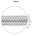
- FIG. 8 is a partial enlarged view of a cut surface (a side surface of the multi-layer substrate) of the multi-layer substrate 1.
- the ground electrode GN having a line width w1 is exposed on the upper surface of the base 10; and the ground electrode GN having a line width w2 is exposed on the lower surface of the resin layer 41.
- the ground electrode GN has plural exposed sections in a direction perpendicular to the insulating layer, so the exposed area of the ground electrode GN in the side surface of the insulating layer is enlarged and thus the connection strength with the metal shield can be further increased.
- inclination angle ⁇ is set so that the ground electrode GN is exposed by a desired line width (so that a desired exposed area of the ground electrode GN is provided).
- the metal shield (conductive shield) 120 is formed by plating in the multi-layer substrate 1 where the sealing layer 110 and ground electrode GN are exposed. As a result, the metal shield 120 and ground electrode GN are electrically connected and at the same time, shielding effect is provided.
- a core is formed using Pd on the surface of the sealing layer 110 and plated copper of 0.5 ⁇ m is formed by electroless plating. Further, copper plating is performed by electrolytic plating to form.the metal shield 120 with dense copper coating of 10 ⁇ m on the sealing layer 110.
- the metal material used to form the metal shield 120 instead of copper (Cu), there can be used a material having a high electric conductivity such as silver (Ag). When the conductor resistance of the metal shield 120 is lowered using such metal material, satisfactory shielding effect can be provided.
- electroless plating is characterized in that coating can be formed on an insulating material and a uniform film can be formed in a section wetted with plating liquid.
- electroless plating is disadvantageous in when the film forming speed is low, it is difficult to form a film of a thickness equal to or less than 3 ⁇ m and when the film thickness is large, internal stress increases and the interface between the mold resin layer and coating layer is easily peeled.
- the film thickness of the formed metal shield 120 is preferably equal to or more than substantially 1 micron.
- the metal shield 120 of copper is formed by electroless plating on the sealing layer 110 and thereafter the metal shield 120 of copper is further formed by electrolytic plating on the resultant surface to make the metal shield 120 more dense, so the connection resistance of the ground electrode GN is lowered to stabilize the ground potential of the metal shield 120 formed on the sealing layer 110, thus enhancing the shielding effect.
- the multi-layer substrate 1 is separated along the cutting reference line S, whereby a plurality of the electronic module 100 illustrated in FIG. 1 are formed.
- the multi-layer substrate 1 i.e., electronic module 100
- a groove has already been formed by cutting, so the separation can be made without using a cutting blade such as a dicing blade.
- the multi-layer substrate 1 may be separated using a cutting blade such as a dicing blade.
- a part of the ground electrode GN is exposed from the side surface of the insulating layers including the resin layers 41, 42 and 43 and then connected at the exposed section with the metal shield 120 acting as a conductive shield, whereby the peripheral edge area, needed in the prior art electronic module, for mounting the ground electrode on the substrate surface is reduced.
- the ground electrode and conductive shield are connected at an outer edge on the lower side of the electronic component mounting area, a connection area between the two parts does not need to be specially provided.
- the insulating layer including the resin layers 41, 42 and 43 are cut in a depth direction to expose the ground electrode GN from the side surface of the insulating layer. Accordingly, a part of the ground electrode is correctly exposed, compared to the prior art in which the level in a depth direction is adjusted and the sealing layer is removed to expose the surface of the ground electrode. Consequently, non-exposure of the ground electrode caused by a cutting misalignment which may occur in the prior art electronic module is reliably eliminated, thus ensuring the connection with the conductive shield and preventing the connection failure between the two parts.
- the substrate is cut so that the side surface of the exposed section of the ground electrode GN in the side surface of the insulating layer including the resin layers 41, 42 and 43 preferably has a prescribed inclination (taper) relative to the direction perpendicular to the insulating layer (a direction perpendicular to the insulating layer plane: normal line direction). Accordingly, the ground electrode GN is cut off at an angle and thus the resultant exposed area is made larger than that obtained when the ground electrode GN is cut off in a perpendicular direction. Thus, the connection area between the ground electrode GN and conductive shield is further enlarged.
- the present embodiment in exposing the ground electrode GN from the side surface of the insulating layer, cutting is performed so that the buried section of the ground electrode GN in the insulating layer including the resin layers 41, 42 and 43 is reached, and thereafter folding is performed along the groove formed by the cutting to separate each of the electronic modules.
- the substrate needs to be again aligned to a reference position set for the separation so as to cut off the substrate.
- the process of separating the electronic module is simplified, considerably improving productivity.
- the present invention is not limited to the above embodiment, and appropriate modifications to the embodiment are possible without departing from the gist of the invention.
- the exposed area of the ground electrode GN is varied by inclination angle ⁇ at which the multi-layer substrate 1 is cut.
- the exposed area of the ground electrode GN may be varied by the number of the exposed ground electrodes GN or the film thickness (refer to FIG. 8 ) of the ground electrode GN.
- the exposed area of the ground electrode GN may be varied by combining the above methods.
- the ground electrode GN to be exposed all the ground electrodes included in the multi-layer substrate 1 can be used, including the ground electrode of the electronic component 60 mounted on the multi-layer substrate 1 and the ground electrode of the semiconductor device 30.
- FIG. 10 is a process diagram illustrating an exemplary fabrication procedure of an electronic module according to a variation 2, and corresponds to FIG. 6 .
- the same reference characters are applied to parts corresponding to those of FIG. 6 , and detailed explanation thereof is omitted.
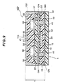
- the metal shield 120' having a substantially constant height h by using vapor deposition, sputtering or the like. After forming such metal shield 120', the substrate is cut off by use of a cutting blade such as a dicing blade along a cutting reference line S. As a result, it is possible to form an electronic module 100' which, as illustrated in FIG. 9 , has a different film thickness depending on the section thereof and has high tolerance against impact from the side surface.
- the metal shield 120 may be formed by a substantially box-shaped metal cap using a metal material such as 42 alloy, kovar, phosphor bronze or iron.
- the metal shield 120 resistance against environment of the module components may be enhanced by forming an antioxidant layer on the surface of the metal film.
- a reflow-resistant resin is used as a coating material; and in order to enhance the degree of adhesion to the wired substrate with solder, for example, a metal layer of Sn, Ni or the like may be formed by plating, sputtering or the like.
- not a plurality of ground electrodes GN but a single ground electrode GN may be provided; and instead of the ground electrode GN, another wiring layer may be formed in the multi-layer substrate 1.
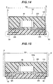
- FIG. 14 is a view illustrating a schematic configuration of an electronic module 100 formed by the multi-layer substrate separation process according to the first embodiment and its variation
- FIG. 15 is a view illustrating a schematic configuration of an electronic module 100a formed by the multi-layer substrate separation process according to a second embodiment.
- the substrate surface in a side on which an electronic component is mounted is referred to as "front surface”; and the substrate surface in an opposite side is referred to as "rear surface”.
- the cutting (what is called a half cutting) is performed by use of a dicing blade or the like along the cutting reference line S while avoiding complete separation from the multi-layer substrate so that a part of the ground electrode GN is exposed; and after the sealing layer 110, metal shield 120 and the like have been formed, the cutoff (what is called a full cutting) or breaking is performed from the upper part of the substrate along the cutting reference line S, whereby the separation is performed.
- the cutoff what is called a full cutting
- breaking is performed from the upper part of the substrate along the cutting reference line S, whereby the separation is performed.
- the width of the electronic module 100 increases by the cutoff portion Sd, resulting in size growth.
- the cutoff portion Sd must be considered, and thus the substantial effective area of the substrate decreases, making it difficult to downsize the module.
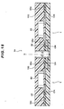
- half cutting is performed from the front surface of the substrate along the cutting reference line S so that a part of the ground electrode GN is exposed, and thereafter an incision is made from the rear surface to the half cutting position by use of a cutoff blade having a blade thickness larger than that of the cutoff blade used for the half cutting, whereby full cutting is performed (refer to FIG. 15 ).
- the bottom end 90 of each electronic module is positioned at an inner side relative to the end of the metal shield 120. Accordingly, the size of the electronic module 100 can be set without considering the cutoff portion Sd protruding to the outside relative to the metal shield 120 as illustrated in FIG. 14 , so the substantial effective area of the substrate can be increased, allowing downsizing of the module.
- cutting reference line S used for separating the electronic modules 100a is indicated by the dashed-dotted line.
- a resist 56a is, as illustrated in FIG. 17 , formed so as to cover a wire 56 of the electronic component 60 mounted on the front surface of the integrated multi-layer substrate 1a, and thereafter a sealing layer 110 composed of epoxy resin is formed so as to cover the whole electronic component 60.
- the integrated multi-layer substrate 1a is half-cut along the reference line S by use of a dicing blade, so that a concave 70 of a depth Dc is formed (refer to FIG. 18 ).
- the depth Dc of the concave 70 may be set to any value as long as the value is, as indicated by formula (1), larger than a depth Db by which a part of the ground electrode GN contained in the integrated multi-layer substrate 1a is exposed. Dc > Db
- electroless plating is performed on the integrated multi-layer substrate 1a having formed therein the concave 70; for example, copper plating of 0.5 ⁇ m is formed by electroless plating. Further, copper plating is performed by electrolytic plating to form the metal shield 120 with dense copper coating of 20 ⁇ m on the sealing layer 110 (refer to FIG. 19 ).
- FIG. 20 is a view illustrating an example of separation process according tq the first embodiment
- FIG. 21 is a view illustrating an example of separation process according to the second embodiment.
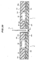
- the full cutting is performed from the front surface using a cutoff blade having a blade thickness smaller than that of the cutoff blade used for the half cutting (refer to formula (2))
- the bottom part of each electronic module 100 obtained by the separation process protrudes to the outside by a cutoff portion Sd (refer to FIG. 14 ).
- the size of the electronic module 100 increases by the cutoff portion Sd.
- the blade thickness of a cutoff blade used for full cutting may be increased; but when the blade thickness is increased, the side surface of the cutoff blade may come into contact with the metal shield 120 during the cutoff, reducing the shield effect.
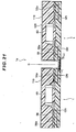
- full cutting is performed from the rear surface using a cutoff blade having a blade thickness larger than that of the cutoff blade used for the half cutting (refer to formula (3)).
- a cutoff blade having a blade thickness larger than that of the cutoff blade used for the half cutting (refer to formula (3)).
- an incision is made along the reference line S from the rear surface to the half cutting position, whereby the cutoff is performed.
- the rear surface of the integrated multi-layer substrate 1a may be marked with an additional reference line for full cutting, so that the cutoff is performed along that reference line.
- the bottom end 90 of each electronic module 100 is, as illustrated in FIG. 15 , positioned at an inner side relative to the end of the metal shield 120. Accordingly, the size of the electronic module 100 can be set without considering the cutoff portion Sd protruding to the outside relative to the metal shield 120 as illustrated in FIG. 14 , so the substantial effective area of the substrate can be increased, allowing downsizing of the module. Further, when the electronic modules 100 are separated after a connection terminal and the like have been arranged on the rear surface of the integrated multi-layer substrate 1a, also, when the full cutting is performed from the rear surface of the integrated multi-layer substrate 1a, the electronic modules can be separated without damaging the connection terminal.
- the electronic module 100 as illustrated in FIG. 15 can be provided.
- the electronic module as illustrated in FIG. 15 can be provided by making an incision only once.
- the half cutting is performed so that the side surface of the exposed section of the ground electrode GN is perpendicular to a direction of the insulating layer plane (for example, refer to FIG. 21 ).
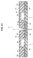
- the half cutting may be performed so that the side surface of the exposed section of the ground electrode GN has a prescribed inclination (taper) relative to a direction perpendicular to the insulating layer (a direction perpendicular to the insulating layer plane: normal line direction), and thereafter the sealing layer 110 and metal shield 120 are formed, and finally the full cutting is performed from the rear surface (refer to FIG. 23 ).
- the ground electrode arranged in the peripheral edge of substrate and its formation area according to the prior art can be reduced to enlarge the mounting area of electronic components, allowing further downsizing by higher mounting density; further the ground electrode and conductive shield can be reliably connected and in addition, connection failure caused by non-exposure of the ground electrode can be prevented, allowing improvement in product reliability, yield rate and productivity.
- the present invention can be applied widely and effectively to the fabrication of an apparatus, equipment, system, various types of devices or the like incorporating an active component such as a semiconductor device, and/or a passive component such as a resistor, capacitor or the like, and particularly to the fabrication of those required to be downsized and have high performance.
Landscapes
- Structures Or Materials For Encapsulating Or Coating Semiconductor Devices Or Solid State Devices (AREA)
- Encapsulation Of And Coatings For Semiconductor Or Solid State Devices (AREA)
Applications Claiming Priority (2)
| Application Number | Priority Date | Filing Date | Title |
|---|---|---|---|
| JP2007172088 | 2007-06-29 | ||
| JP2008153261A JP2009033114A (ja) | 2007-06-29 | 2008-06-11 | 電子モジュール、及び電子モジュールの製造方法 |
Publications (1)
| Publication Number | Publication Date |
|---|---|
| EP2009692A1 true EP2009692A1 (de) | 2008-12-31 |
Family
ID=39870597
Family Applications (1)
| Application Number | Title | Priority Date | Filing Date |
|---|---|---|---|
| EP08011741A Withdrawn EP2009692A1 (de) | 2007-06-29 | 2008-06-27 | Elektronisches Modul und Herstellungsverfahren dafür |
Country Status (2)
| Country | Link |
|---|---|
| US (1) | US20090002967A1 (de) |
| EP (1) | EP2009692A1 (de) |
Cited By (1)
| Publication number | Priority date | Publication date | Assignee | Title |
|---|---|---|---|---|
| EP2573811A3 (de) * | 2011-09-26 | 2014-03-26 | SAE Magnetics (H.K.) Ltd. | Modul mit elektronischen Komponenten und Herstellungsverfahren |
Families Citing this family (26)
| Publication number | Priority date | Publication date | Assignee | Title |
|---|---|---|---|---|
| US20100020518A1 (en) * | 2008-07-28 | 2010-01-28 | Anadigics, Inc. | RF shielding arrangement for semiconductor packages |
| TWI381510B (zh) * | 2008-10-07 | 2013-01-01 | 日月光半導體製造股份有限公司 | 具有屏蔽蓋體之晶片封裝結構 |
| JP2010192653A (ja) * | 2009-02-18 | 2010-09-02 | Panasonic Corp | 半導体装置 |
| JP2010225620A (ja) * | 2009-03-19 | 2010-10-07 | Panasonic Corp | 回路モジュール |
| US9362196B2 (en) | 2010-07-15 | 2016-06-07 | Kabushiki Kaisha Toshiba | Semiconductor package and mobile device using the same |
| US8966747B2 (en) * | 2011-05-11 | 2015-03-03 | Vlt, Inc. | Method of forming an electrical contact |
| US8669646B2 (en) * | 2011-05-31 | 2014-03-11 | Broadcom Corporation | Apparatus and method for grounding an IC package lid for EMI reduction |
| JP5703245B2 (ja) | 2012-02-28 | 2015-04-15 | 株式会社東芝 | 無線装置、それを備えた情報処理装置および記憶装置 |
| JP5710558B2 (ja) | 2012-08-24 | 2015-04-30 | 株式会社東芝 | 無線装置、それを備えた情報処理装置及び記憶装置 |
| US9419667B2 (en) | 2013-04-16 | 2016-08-16 | Skyworks Solutions, Inc. | Apparatus and methods related to conformal coating implemented with surface mount devices |
| JP5756500B2 (ja) * | 2013-08-07 | 2015-07-29 | 太陽誘電株式会社 | 回路モジュール |
| JP2015072935A (ja) * | 2013-09-03 | 2015-04-16 | 太陽誘電株式会社 | 回路モジュール及びその製造方法 |
| JP6418625B2 (ja) * | 2013-12-13 | 2018-11-07 | 東芝メモリ株式会社 | 半導体装置の製造方法 |
| CN204632754U (zh) | 2015-03-18 | 2015-09-09 | 新科实业有限公司 | 电子部件模块 |
| JP2017017238A (ja) * | 2015-07-03 | 2017-01-19 | 株式会社ジェイデバイス | 半導体装置及びその製造方法 |
| JP2017162989A (ja) * | 2016-03-09 | 2017-09-14 | イビデン株式会社 | 電子部品内蔵基板およびその製造方法 |
| JP6728917B2 (ja) | 2016-04-12 | 2020-07-22 | Tdk株式会社 | 電子回路モジュールの製造方法 |
| KR20190067839A (ko) * | 2016-10-04 | 2019-06-17 | 스카이워크스 솔루션즈, 인코포레이티드 | 오버몰드 구조를 갖는 양면 라디오-주파수 패키지 |
| JP6408540B2 (ja) * | 2016-12-01 | 2018-10-17 | 太陽誘電株式会社 | 無線モジュール及び無線モジュールの製造方法 |
| JP6463323B2 (ja) * | 2016-12-01 | 2019-01-30 | 太陽誘電株式会社 | 無線モジュール、およびその製造方法 |
| US10541209B2 (en) * | 2017-08-03 | 2020-01-21 | General Electric Company | Electronics package including integrated electromagnetic interference shield and method of manufacturing thereof |
| US11398424B2 (en) * | 2020-02-18 | 2022-07-26 | Advanced Semiconductor Engineering, Inc. | Semiconductor package structure |
| WO2021205930A1 (ja) * | 2020-04-07 | 2021-10-14 | 株式会社村田製作所 | モジュール |
| WO2021251160A1 (ja) * | 2020-06-10 | 2021-12-16 | 株式会社村田製作所 | モジュールおよび部品 |
| CN219395186U (zh) | 2020-06-22 | 2023-07-21 | 株式会社村田制作所 | 电子部件 |
| US12490416B2 (en) * | 2022-12-08 | 2025-12-02 | Bae Systems Information And Electronic Systems Integration Inc. | Thermally dissipative electromagnetic interference shield or cover for an electronic device |
Citations (7)
| Publication number | Priority date | Publication date | Assignee | Title |
|---|---|---|---|---|
| JPH0514015A (ja) * | 1991-07-03 | 1993-01-22 | Tdk Corp | 高周波smdモジユール |
| JPH0590430A (ja) * | 1991-09-13 | 1993-04-09 | Nec Corp | 大規模集積回路 |
| JP2004193187A (ja) | 2002-12-09 | 2004-07-08 | Matsushita Electric Ind Co Ltd | モジュール部品の製造方法 |
| US20060266547A1 (en) * | 2005-05-25 | 2006-11-30 | Alps Electric Co., Ltd. | Shielded electronic circuit unit and method of manufacturing the same |
| WO2007060784A1 (ja) * | 2005-11-28 | 2007-05-31 | Murata Manufacturing Co., Ltd. | 回路モジュールの製造方法および回路モジュール |
| JP2007172088A (ja) | 2005-12-20 | 2007-07-05 | Osaka Sealing Printing Co Ltd | ストラップ連続体、インレット連続体及びicラベル連続体の製造方法 |
| JP2008153261A (ja) | 2006-12-14 | 2008-07-03 | Mitsubishi Electric Corp | レーザアニール装置 |
Family Cites Families (3)
| Publication number | Priority date | Publication date | Assignee | Title |
|---|---|---|---|---|
| US6803324B2 (en) * | 2001-01-31 | 2004-10-12 | Sony Corporation | Semiconductor device and its manufacturing method |
| US7187060B2 (en) * | 2003-03-13 | 2007-03-06 | Sanyo Electric Co., Ltd. | Semiconductor device with shield |
| US7030469B2 (en) * | 2003-09-25 | 2006-04-18 | Freescale Semiconductor, Inc. | Method of forming a semiconductor package and structure thereof |
-
2008
- 2008-06-27 US US12/216,043 patent/US20090002967A1/en not_active Abandoned
- 2008-06-27 EP EP08011741A patent/EP2009692A1/de not_active Withdrawn
Patent Citations (8)
| Publication number | Priority date | Publication date | Assignee | Title |
|---|---|---|---|---|
| JPH0514015A (ja) * | 1991-07-03 | 1993-01-22 | Tdk Corp | 高周波smdモジユール |
| JPH0590430A (ja) * | 1991-09-13 | 1993-04-09 | Nec Corp | 大規模集積回路 |
| JP2004193187A (ja) | 2002-12-09 | 2004-07-08 | Matsushita Electric Ind Co Ltd | モジュール部品の製造方法 |
| US20060266547A1 (en) * | 2005-05-25 | 2006-11-30 | Alps Electric Co., Ltd. | Shielded electronic circuit unit and method of manufacturing the same |
| WO2007060784A1 (ja) * | 2005-11-28 | 2007-05-31 | Murata Manufacturing Co., Ltd. | 回路モジュールの製造方法および回路モジュール |
| US20080210462A1 (en) * | 2005-11-28 | 2008-09-04 | Murata Manufacturing Co., Ltd. | Method for manufacturing circuit modules and circuit module |
| JP2007172088A (ja) | 2005-12-20 | 2007-07-05 | Osaka Sealing Printing Co Ltd | ストラップ連続体、インレット連続体及びicラベル連続体の製造方法 |
| JP2008153261A (ja) | 2006-12-14 | 2008-07-03 | Mitsubishi Electric Corp | レーザアニール装置 |
Cited By (1)
| Publication number | Priority date | Publication date | Assignee | Title |
|---|---|---|---|---|
| EP2573811A3 (de) * | 2011-09-26 | 2014-03-26 | SAE Magnetics (H.K.) Ltd. | Modul mit elektronischen Komponenten und Herstellungsverfahren |
Also Published As
| Publication number | Publication date |
|---|---|
| US20090002967A1 (en) | 2009-01-01 |
Similar Documents
| Publication | Publication Date | Title |
|---|---|---|
| US20090002967A1 (en) | Electronic module and fabrication method thereof | |
| KR101004275B1 (ko) | 전자 모듈 및 전자 모듈의 제조 방법 | |
| US7514772B2 (en) | Method of manufacturing a semiconductor apparatus | |
| CN111326428B (zh) | 具有开放端子的屏蔽半导体封装及制造的方法 | |
| US6803324B2 (en) | Semiconductor device and its manufacturing method | |
| JP5141076B2 (ja) | 半導体装置 | |
| US7816783B2 (en) | Resin wiring substrate, and semiconductor device and laminated semiconductor device using the same | |
| US20150131231A1 (en) | Electronic component module and manufacturing method thereof | |
| JP2009218484A (ja) | 電子モジュール、および電子モジュールの製造方法 | |
| JP7494432B2 (ja) | 電子素子モジュール及びその製造方法 | |
| JP6408540B2 (ja) | 無線モジュール及び無線モジュールの製造方法 | |
| US9338886B2 (en) | Substrate for mounting semiconductor, semiconductor device and method for manufacturing semiconductor device | |
| JP2020145394A (ja) | 電子素子モジュール及びその製造方法 | |
| CN117979538A (zh) | 电路板 | |
| KR20200123572A (ko) | 전자 소자 모듈 및 그 제조 방법 | |
| KR20040040348A (ko) | 회로 장치, 회로 모듈 및 회로 장치의 제조 방법 | |
| KR20150135048A (ko) | 인쇄회로기판, 인쇄회로기판의 제조 방법 및 이를 포함하는 적층형 패키지 | |
| US11127689B2 (en) | Segmented shielding using wirebonds | |
| US7816777B2 (en) | Semiconductor-element mounting substrate, semiconductor device, and electronic equipment | |
| US10667419B2 (en) | Manufacturing method of an electronic component module | |
| US10879184B2 (en) | Electronic device mounting board, electronic package, and electronic module | |
| KR20210131689A (ko) | 전자 소자 모듈 및 그 제조 방법 | |
| US20080290514A1 (en) | Semiconductor device package and method of fabricating the same | |
| KR101741648B1 (ko) | 전자파 차폐 수단을 갖는 반도체 패키지 및 그 제조 방법 | |
| US10356911B2 (en) | Electronic device module and method of manufacturing the same |
Legal Events
| Date | Code | Title | Description |
|---|---|---|---|
| PUAI | Public reference made under article 153(3) epc to a published international application that has entered the european phase |
Free format text: ORIGINAL CODE: 0009012 |
|
| 17P | Request for examination filed |
Effective date: 20080627 |
|
| AK | Designated contracting states |
Kind code of ref document: A1 Designated state(s): AT BE BG CH CY CZ DE DK EE ES FI FR GB GR HR HU IE IS IT LI LT LU LV MC MT NL NO PL PT RO SE SI SK TR |
|
| AX | Request for extension of the european patent |
Extension state: AL BA MK RS |
|
| 17Q | First examination report despatched |
Effective date: 20090330 |
|
| AKX | Designation fees paid |
Designated state(s): AT BE BG CH CY CZ DE DK EE ES FI FR GB GR HR HU IE IS IT LI LT LU LV MC MT NL NO PL PT RO SE SI SK TR |
|
| RAP1 | Party data changed (applicant data changed or rights of an application transferred) |
Owner name: TDK CORPORATION |
|
| RAP1 | Party data changed (applicant data changed or rights of an application transferred) |
Owner name: TDK CORPORATION |
|
| STAA | Information on the status of an ep patent application or granted ep patent |
Free format text: STATUS: THE APPLICATION IS DEEMED TO BE WITHDRAWN |
|
| 18D | Application deemed to be withdrawn |
Effective date: 20160105 |