EP2009694A2 - Halbleiterbauelement und Herstellungsverfahren dafür - Google Patents
Halbleiterbauelement und Herstellungsverfahren dafür Download PDFInfo
- Publication number
- EP2009694A2 EP2009694A2 EP08010529A EP08010529A EP2009694A2 EP 2009694 A2 EP2009694 A2 EP 2009694A2 EP 08010529 A EP08010529 A EP 08010529A EP 08010529 A EP08010529 A EP 08010529A EP 2009694 A2 EP2009694 A2 EP 2009694A2
- Authority
- EP
- European Patent Office
- Prior art keywords
- layer
- crystal semiconductor
- substrate
- semiconductor layer
- semiconductor device
- Prior art date
- Legal status (The legal status is an assumption and is not a legal conclusion. Google has not performed a legal analysis and makes no representation as to the accuracy of the status listed.)
- Withdrawn
Links
Images


Classifications
-
- H—ELECTRICITY
- H10—SEMICONDUCTOR DEVICES; ELECTRIC SOLID-STATE DEVICES NOT OTHERWISE PROVIDED FOR
- H10D—INORGANIC ELECTRIC SEMICONDUCTOR DEVICES
- H10D86/00—Integrated devices formed in or on insulating or conducting substrates, e.g. formed in silicon-on-insulator [SOI] substrates or on stainless steel or glass substrates
-
- H—ELECTRICITY
- H10—SEMICONDUCTOR DEVICES; ELECTRIC SOLID-STATE DEVICES NOT OTHERWISE PROVIDED FOR
- H10D—INORGANIC ELECTRIC SEMICONDUCTOR DEVICES
- H10D30/00—Field-effect transistors [FET]
- H10D30/60—Insulated-gate field-effect transistors [IGFET]
- H10D30/67—Thin-film transistors [TFT]
- H10D30/674—Thin-film transistors [TFT] characterised by the active materials
- H10D30/6741—Group IV materials, e.g. germanium or silicon carbide
- H10D30/6748—Group IV materials, e.g. germanium or silicon carbide having a multilayer structure or superlattice structure
-
- H—ELECTRICITY
- H10—SEMICONDUCTOR DEVICES; ELECTRIC SOLID-STATE DEVICES NOT OTHERWISE PROVIDED FOR
- H10D—INORGANIC ELECTRIC SEMICONDUCTOR DEVICES
- H10D30/00—Field-effect transistors [FET]
- H10D30/60—Insulated-gate field-effect transistors [IGFET]
- H10D30/791—Arrangements for exerting mechanical stress on the crystal lattice of the channel regions
- H10D30/796—Arrangements for exerting mechanical stress on the crystal lattice of the channel regions having memorised stress for introducing strain in the channel regions, e.g. recrystallised polysilicon gates
-
- H—ELECTRICITY
- H10—SEMICONDUCTOR DEVICES; ELECTRIC SOLID-STATE DEVICES NOT OTHERWISE PROVIDED FOR
- H10D—INORGANIC ELECTRIC SEMICONDUCTOR DEVICES
- H10D30/00—Field-effect transistors [FET]
- H10D30/60—Insulated-gate field-effect transistors [IGFET]
- H10D30/791—Arrangements for exerting mechanical stress on the crystal lattice of the channel regions
- H10D30/798—Arrangements for exerting mechanical stress on the crystal lattice of the channel regions being provided in or under the channel regions
-
- H—ELECTRICITY
- H10—SEMICONDUCTOR DEVICES; ELECTRIC SOLID-STATE DEVICES NOT OTHERWISE PROVIDED FOR
- H10D—INORGANIC ELECTRIC SEMICONDUCTOR DEVICES
- H10D86/00—Integrated devices formed in or on insulating or conducting substrates, e.g. formed in silicon-on-insulator [SOI] substrates or on stainless steel or glass substrates
- H10D86/01—Manufacture or treatment
- H10D86/021—Manufacture or treatment of multiple TFTs
- H10D86/0212—Manufacture or treatment of multiple TFTs comprising manufacture, treatment or coating of substrates
-
- H—ELECTRICITY
- H10—SEMICONDUCTOR DEVICES; ELECTRIC SOLID-STATE DEVICES NOT OTHERWISE PROVIDED FOR
- H10D—INORGANIC ELECTRIC SEMICONDUCTOR DEVICES
- H10D86/00—Integrated devices formed in or on insulating or conducting substrates, e.g. formed in silicon-on-insulator [SOI] substrates or on stainless steel or glass substrates
- H10D86/01—Manufacture or treatment
- H10D86/021—Manufacture or treatment of multiple TFTs
- H10D86/0214—Manufacture or treatment of multiple TFTs using temporary substrates
-
- H—ELECTRICITY
- H10—SEMICONDUCTOR DEVICES; ELECTRIC SOLID-STATE DEVICES NOT OTHERWISE PROVIDED FOR
- H10D—INORGANIC ELECTRIC SEMICONDUCTOR DEVICES
- H10D86/00—Integrated devices formed in or on insulating or conducting substrates, e.g. formed in silicon-on-insulator [SOI] substrates or on stainless steel or glass substrates
- H10D86/40—Integrated devices formed in or on insulating or conducting substrates, e.g. formed in silicon-on-insulator [SOI] substrates or on stainless steel or glass substrates characterised by multiple TFTs
- H10D86/60—Integrated devices formed in or on insulating or conducting substrates, e.g. formed in silicon-on-insulator [SOI] substrates or on stainless steel or glass substrates characterised by multiple TFTs wherein the TFTs are in active matrices
-
- H—ELECTRICITY
- H10—SEMICONDUCTOR DEVICES; ELECTRIC SOLID-STATE DEVICES NOT OTHERWISE PROVIDED FOR
- H10P—GENERIC PROCESSES OR APPARATUS FOR THE MANUFACTURE OR TREATMENT OF DEVICES COVERED BY CLASS H10
- H10P90/00—Preparation of wafers not covered by a single main group of this subclass, e.g. wafer reinforcement
- H10P90/19—Preparing inhomogeneous wafers
- H10P90/1904—Preparing vertically inhomogeneous wafers
- H10P90/1906—Preparing SOI wafers
- H10P90/1914—Preparing SOI wafers using bonding
- H10P90/1916—Preparing SOI wafers using bonding with separation or delamination along an ion implanted layer, e.g. Smart-cut
-
- H—ELECTRICITY
- H10—SEMICONDUCTOR DEVICES; ELECTRIC SOLID-STATE DEVICES NOT OTHERWISE PROVIDED FOR
- H10W—GENERIC PACKAGES, INTERCONNECTIONS, CONNECTORS OR OTHER CONSTRUCTIONAL DETAILS OF DEVICES COVERED BY CLASS H10
- H10W10/00—Isolation regions in semiconductor bodies between components of integrated devices
- H10W10/10—Isolation regions comprising dielectric materials
- H10W10/181—Semiconductor-on-insulator [SOI] isolation regions, e.g. buried oxide regions of SOI wafers
Definitions
- the present invention relates to a semiconductor device including a thin film transistor over an insulating surface and a manufacturing method thereof.
- An integrated circuit has been developed, which uses a semiconductor substrate called a silicon-on-insulator (hereinafter also referred to as SOI) which has a thin single-crystal semiconductor layer over an insulating surface, instead of a silicon wafer which is manufactured by thinly slicing an ingot of a single-crystal semiconductor.
- SOI silicon-on-insulator
- An integrated circuit using an SOI substrate has attracted attention as a circuit which reduces parasitic capacitance between source and drain regions of the transistor and the substrate, and improves performance of the integrated circuit.
- a hydrogen ion implantation separation method is a method in which the surface of a silicon wafer is irradiated with hydrogen ions to form a weakened layer at a predetermined depth from the surface of the wafer, a thin silicon layer (a semiconductor layer) which is thinner than the silicon wafer is separated by heat treatment or the like with the weakened layer used as a separation plane (a cleavage plane), and the thin silicon layer (the semiconductor layer) is attached and bonded to another silicon wafer.
- a semiconductor device in which a single-crystal semiconductor layer is formed over an insulating substrate such as a high heat-resistant glass substrate is disclosed (e.g., see Reference 2: Japanese Published Patent Application No. H11-163363 ).
- the semiconductor device has a structure in which the entire surface of the glass substrate is protected by an insulating silicon film and the thin single-crystal semiconductor layer obtained by the hydrogen ion implantation separation method is firmly fixed over the insulating silicon film.
- the present invention provides a semiconductor device in which a semiconductor layer having favorable crystallinity and having tensile strain or compressive strain is efficiently and surely formed over an insulating substrate formed using glass, plastic, or the like, and a manufacturing method thereof.
- a semiconductor device of the present invention includes a first circuit group and a second circuit group provided over a base substrate having an insulating surface.
- the first circuit group includes a first transistor having a first single-crystal semiconductor layer as an active layer.
- the second circuit group includes a second transistor having a second single-crystal semiconductor layer as an active layer.
- a bonding layer is provided between each of the first single-crystal semiconductor layer and the second single-crystal semiconductor layer and the base substrate having an insulating surface.
- the second single-crystal semiconductor layer is a single-crystal silicon layer having compressive strain.
- a semiconductor device of the present invention includes a first circuit group and a second circuit group provided over a base substrate having an insulating surface.
- the first circuit group includes a first transistor having a first single-crystal semiconductor layer as an active layer.
- the second circuit group includes a second transistor having a second single-crystal semiconductor layer as an active layer.
- a bonding layer is provided between each of the first single-crystal semiconductor layer and the second single-crystal semiconductor layer is provided and the base substrate having an insulating surface.
- the first single-crystal semiconductor layer is a single-crystal silicon layer having tensile strain.
- the second single-crystal semiconductor layer is a single-crystal silicon layer having compressive strain.
- the first circuit group include at least one of a data driver, a scan driver, and a logic circuit of a display device
- the second circuit group include a pixel portion of the display device
- the pixel portion of the display device may include an EL element and the second transistor may be a transistor controlling supply of current to the EL element.
- the pixel portion of the display device may include a liquid crystal element and the second transistor may be a transistor controlling application of voltage to the liquid crystal element.
- a method for manufacturing a semiconductor device of the present invention includes the following steps: irradiating the surface of a semiconductor substrate with an ion to form a weakened layer (a separation layer) inside the semiconductor substrate; separating a single-crystal semiconductor layer from the semiconductor substrate with the weakened layer used as a separation surface; bonding the single-crystal semiconductor layer over a base substrate with a bonding layer interposed therebetween; and generating heat shrink by heat treatment of the base substrate to generate compressive strain in the single-crystal semiconductor layer.
- a method for manufacturing a semiconductor device of the present invention includes the following steps: irradiating the surface of a semiconductor substrate with an ion to form a weakened layer (a separation layer) inside the semiconductor substrate; separating a single-crystal semiconductor layer from the semiconductor substrate with the weakened layer used as a separation surface; bonding the single-crystal semiconductor layer over a base substrate with a bonding layer interposed therebetween; and bonding a single-crystal semiconductor layer having tensile strain over the base substrate with the bonding layer interposed between after generating heat shrink by heat treatment of the base substrate to generate compressive strain in the single-crystal semiconductor layer.
- a silicon oxide film or the like formed using an organic silane gas by a chemical vapor deposition method is typically used as the bonding layer.
- the base substrate is preferably formed using a light-transmitting material.
- a transistor using a single-crystal semiconductor layer as an active layer and a transistor using a single-crystal semiconductor layer having compressive strain as an active layer are formed over the same insulating substrate formed using glass, plastic, or the like.
- a transistor using a single-crystal semiconductor layer having tensile strain as an active layer and a transistor using a single-crystal semiconductor layer having compressive strain as an active layer are formed over the same insulating substrate formed using glass, plastic, or the like.
- Polarities of transistors which lead to improvement in mobility are different between the case where tensile strain is applied to a semiconductor layer and the case where compressive strain is applied to a semiconductor layer.
- tensile strain or compressive strain can be applied to a semiconductor layer formed over a substrate, whereas a semiconductor layer to which appropriate strain is applied by the present invention can be formed in a desired region in an attachment step.
- the step of applying compressive strain to the semiconductor layer is a step utilizing part of shrink by heat treatment of the substrate, which has been performed conventionally, without adding any new step, and can be realized extremely easily, which is a great advantage.
- FIGS. 1A to 6C A method for manufacturing a semiconductor device of the present invention is described with reference to FIGS. 1A to 6C .
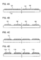
- FIGS. 2A to 2E and FIGS. 3A to 3D A method for providing a single-crystal semiconductor layer over a substrate having an insulating surface is described with reference to FIGS. 2A to 2E and FIGS. 3A to 3D .
- a semiconductor substrate 108 shown in FIG 2A is cleaned, and ions which are accelerated by an electric field are introduced into the semiconductor substrate 108 from the surface thereof to reach a predetermined depth to form a weakened layer (a separation layer) 110.
- Ion irradiation is performed in consideration of the thickness of a single-crystal semiconductor layer which is formed over a base substrate.
- the thickness of the single-crystal semiconductor layer is preferably equal to or greater than 1 ⁇ m and equal to or less than 3 ⁇ m. Accelerating voltage for irradiating the semiconductor substrate 108 with ions is set in consideration of such a thickness.
- a p-type or n-type single-crystal silicon substrate (silicon wafer) is typically used as the semiconductor substrate 108.
- a substrate of silicon or germanium, or a substrate of a compound semiconductor such as gallium arsenide or indium phosphide can be used as another single-crystal semiconductor substrate.
- a method in which a single-crystal semiconductor substrate is irradiated with ions of hydrogen or fluorine to reach a predetermined depth and then heat treatment is performed to separate a surface layer of a single-crystal silicon layer is used in this embodiment mode
- a method in which epitaxial growth of single-crystal silicon is performed over a porous silicon layer and then the porous silicon layer is separated by water jet may be used.
- the weakened layer 110 is formed by introducing ions of hydrogen, helium, or halogen typified by fluorine into the semiconductor substrate 108 by an ion-doping method or an ion implantation method.
- ions of hydrogen, helium, or halogen typified by fluorine
- BF 3 may be used as a source gas.
- an ion implantation method refers to a method in which an ionized gas is separated by mass to introduce desired ions into a semiconductor layer.
- halogen ions such as fluorine ions
- the semiconductor substrate e.g., single-crystal silicon substrate
- fluorine knocks out (expels) silicon atoms in a crystal lattice of silicon to effectively form a vacant portion, so that a minute void is formed in the weakened layer 110.
- the volume of the minute void formed in the weakened layer 110 is changed by heat treatment at relatively low temperature, and a thin single-crystal semiconductor layer can be formed by separation along the weakened layer 110.
- irradiation with hydrogen ions may be performed so that hydrogen is contained in the void.
- the weakened layer 110 which is formed to separate a thin semiconductor layer from the semiconductor substrate 108 utilizes change in the volume of the minute void formed in the weakened layer 110.
- the hydrogen ions preferably include H + , H 2 + , and H 3 + ions with a high proportion of H 3 + ions.
- H 3 + ions With a high proportion of H 3 + ions, irradiation efficiency can be increased and irradiation time can be shortened. With such a structure, separation can be easily performed.
- a protective film against irradiation with ions may be provided on a surface with which ions are irradiated by using a silicon nitride layer, a silicon nitride oxide layer, or the like with a thickness of 50 to 200 nm.
- thermal oxidation general dry oxidation may be performed; however, oxidation in an oxidizing atmosphere to which halogen is added is preferably performed.
- heat treatment is performed at a temperature of higher than or equal to 700 °C in an atmosphere containing HCl by 0.5 to 10 volume% (preferably 3 volume%) with respect to oxygen.
- the heat oxidation is preferably performed at a temperature of 950 to 1100 °C.
- Processing time may be 0.1 to 6 hours, preferably 0.5 to 1 hour.
- the film thickness of an oxide film which is to be formed is 10 to 1000 nm (preferably 50 to 200 nm), for example, 100 nm.
- HCl As well as HCl, one or a plurality of kinds selected from HF, NF 3 , HBr, Cl 2 , ClF 3 , BCl 3 , F 2 , Br 2 , or the like can be used as a compound containing halogen.
- Gettering particularly has an effect of removing a metal impurity. That is, an impurity such as metal turns into a volatile chloride, and then is diffused into a gas phase to be removed by the action of chlorine.
- the above-described heat treatment is effective for the semiconductor substrate 108, the surface of which is treated with chemical mechanical polishing (CMP).
- CMP chemical mechanical polishing
- hydrogen has an effect of compensating defects at an interface between the semiconductor substrate 108 and the oxide film which is to be formed so as to reduce localized level density of the interface, so that the interface between the semiconductor substrate 108 and the oxide film is inactivated, so that electric characteristics are stabilized.
- the oxide film formed by this heat treatment can contain halogen.
- halogen is contained at a concentration of 1 ⁇ 10 17 to 5 ⁇ 10 20 /cm 3
- the oxide film can have a function as a protective film which captures an impurity such as metal and prevents contamination of the semiconductor substrate 108.
- a silicon oxide film is formed as a bonding layer 104 on the surface of the semiconductor substrate 108, which forms a bond with a base substrate 101.
- a silicon oxide film formed using an organic silane gas by a chemical vapor deposition method is preferable.
- a silicon oxide film formed using a silane gas by a chemical vapor deposition method can be used.
- Film formation by a chemical vapor deposition method is performed at a temperature of, for example, 100 to 400 °C, preferably 200 to 350 °C, at which degassing of the weakened layer 110 which is formed in the single-crystal semiconductor substrate 108 does not occur.
- Heat treatment for separating a single-crystal semiconductor layer 102 from the semiconductor substrate 108 is performed at a higher heat treatment temperature (e.g., a temperature of 400 to 600 °C) than temperature for film formation.
- the bonding layer 104 has a smooth surface and forms a hydrophilic surface.
- a silicon oxide film is suitable for the bonding layer 104.
- a silicon oxide film formed using an organic silane gas by a chemical vapor deposition method is preferable.
- an organic silane gas a silicon-containing compound such as tetraethoxysilane (TEOS) (chemical formula: Si(OC 2 H 5 ) 4 ), trimethylsilane (TMS) (chemical formula: (CH 3 ) 3 SiH), tetramethylsilane (chemical formula: Si(CH 3 ) 4 ), tetramethylcyclotetrasiloxane (TMCTS), octamethylcyclotetrasiloxane (OMCTS), hexamethyldisilazane (HMDS), triethoxysilane (chemical formula: SiH(OC 2 H 5 ) 3 ), or trisdimethylaminosilane (chemical formula: SiH(N(CH 3 ) 2 ) 3
- the bonding layer 104 which has a smooth surface and forms a hydrophilic surface is provided with a thickness of 5 to 500 nm. With such a thickness, roughness of a surface on which the bonding layer 104 is formed can be smoothed and smoothness of a growth surface of the film can be ensured. Further, distortion between the single-crystal semiconductor layer 102 and a substrate which are bonded to each other can be reduced.
- the base substrate 101 may be provided with a similar silicon oxide film.
- the single-crystal semiconductor layer 102 when the single-crystal semiconductor layer 102 is bonded to the base substrate 101, the single-crystal semiconductor layer 102 and the base substrate 101 can be firmly bonded to each other when the bonding layer 104 formed of a silicon oxide layer which is preferably formed using organic silane as a material is provided on either one or both surfaces of the base substrate 101 and the single-crystal semiconductor layer 102 which are to be bonded.
- FIG. 2C shows a mode in which a surface of the base substrate 101 and a surface of the semiconductor substrate 108, on which the bonding layer 104 is formed, are disposed in contact to be bonded to each other.
- the surfaces which are to be bonded are cleaned sufficiently.
- a bond is formed. This bond is formed by Van der Waals force.
- a stronger bond can be formed by hydrogen bonding.
- the surfaces which are to form a bond may be activated.
- the surfaces which are to form a bond are irradiated with an atomic beam or an ion beam.
- an atomic beam or an ion beam an inert gas neutral atom beam or inert gas ion beam of argon or the like can be used.
- plasma irradiation or radical treatment may be performed. With such a surface treatment, a bond between different kinds of materials can be easily formed even at a temperature of 200 to 400 °C.
- a step of separating the single-crystal semiconductor layer 102 from the semiconductor substrate 108 and a step of bonding the base substrate 101 and the single-crystal semiconductor layer 102 firmly may be performed by separate heat treatments or may be simultaneously performed by one heat treatment.
- heat treatment or pressure treatment is preferably performed.
- bonding strength can be increased.
- Pressure treatment is performed so that pressure is applied in a perpendicular direction to the bonded surface, in consideration of pressure resistance of the base substrate 101 and the semiconductor substrate 108.
- heat treatment is performed to separate the semiconductor substrate 108 from the base substrate 101 with part of the weakened layer 110 used as a separation plane.
- heat treatment is performed at 400 to 600 °C, the volume of minute voids formed in the weakened layer 110 is changed, so that separation can be performed along the weakened layer 110.
- the heat treatment is preferably performed at a temperature lower than the temperature at which heat treatment is performed on the base substrate 101 in advance. Since the bonding layer 104 is bonded to the base substrate 101, the single-crystal semiconductor layer 102 having the same crystallinity as the semiconductor substrate 108 remains over the base substrate 101.
- heat treatment is performed on the base substrate 101 to which the single-crystal semiconductor layer 102 is bonded.
- the heat treatment at this time is preferably performed at a temperature lower than the temperature at which heat treatment is performed on the base substrate 101 in advance and higher than the temperature of the heat treatment at the time of separation.
- the base substrate 101 slightly generates heat shrink and applies compressive strain to the single-crystal semiconductor layer 102 bonded over the base substrate 101.
- the temperature of the heat treatment is preferably adjusted as appropriate in accordance with a material of the base substrate.
- FIG 3A shows a step in which the semiconductor substrate 108 provided with a silicon oxide film 121 is irradiated with ions which are accelerated by an electric field to reach a predetermined depth to form the weakened layer 110. Ion irradiation is similar to that shown in FIG 2A .
- the silicon oxide film 121 is formed on the surface of the semiconductor substrate 108, the surface can be prevented from being damaged and from losing smoothness due to ion irradiation. Further, the silicon oxide film 121 has an effect of preventing diffusion of impurities against the single-crystal semiconductor layer 102 which is formed of the semiconductor substrate 108.
- FIG. 3B shows a step in which the base substrate 101, over which a blocking layer 109 and the bonding layer 104 are formed, and a surface of the semiconductor substrate 108, on which the silicon oxide film 121 formed, are disposed in contact with each other to be bonded.
- the semiconductor substrate 108 is separated, as shown in FIG. 3C .
- Heat treatment for separating the single-crystal semiconductor layer 102 is performed in a manner similar to that shown in FIG. 2D .
- the heat treatment in a bonding-separating process is performed at a temperature lower than or equal to the temperature at which the heat treatment is performed on the base substrate 101 in advance.
- the semiconductor substrate shown in FIG. 3C can be obtained.
- heat treatment is performed on the base substrate 101 to which the single-crystal semiconductor layer 102 is bonded.
- the heat treatment at this time is preferably performed at a temperature lower than the temperature at which heat treatment is performed on the base substrate 101 in advance and higher than the temperature of the heat treatment at the time of separation.
- the base substrate 101 slightly generates heat shrink and applies compressive strain to the single-crystal semiconductor layer 102 bonded over the base substrate 101.
- the temperature of the heat treatment is preferably adjusted as appropriate in accordance with a material of the base substrate.
- a substrate having an insulating surface can be used as the base substrate 101.
- any of various glass substrates which are used in the electronics industry and referred to as non-alkali glass substrates such as aluminoborosilicate glass substrates, aluminosilicate glass substrates, and barium borosilicate glass substrates can be used.
- a quartz substrate may be used.
- a substrate having a suitable transition point may be used in accordance with the temperature of the heat treatment.
- a different single-crystal semiconductor layer is further formed, so that a normal single-crystal semiconductor layer and a single-crystal semiconductor layer to which compressive strain is applied can be formed over the same substrate.
- conditions and the like of a step in which the single-crystal semiconductor layer having tensile strain is grown over the silicon germanium layer having reduced stress by utilizing difference of lattice constants are not particularly limited to certain conditions in the present invention.
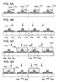
- a resist pattern having a desired shape is formed by using a photomask, and island-shaped semiconductor layers 151, 152, 161, and 162 are formed by processing using photolithography, as shown in FIG 4B .
- end portions of the semiconductor layers 151, 152, 161, and 162 are each formed to have a tilt angle (a taper angle).
- the reason for forming each of the end portions of the semiconductor layers 151, 152, 161, and 162 to have a taper angle is that an advantageous effect of improving coverage of a semiconductor layer of an insulating film which is formed later can be expected, for example.
- this taper angle is small, a parasitic transistor whose characteristics are different from those of a center portion of each of the semiconductor layers 151, 152, 161, and 162 is formed in a taper region in some cases.
- the taper angle is preferably large. Therefore, it is preferable that the taper angle be approximately 45 to 90 degrees.
- an end portion of the semiconductor layer corresponds to an edge portion of the semiconductor layer formed to have an island shape.
- a side surface of the semiconductor layer corresponds to the surface of the edge portion.
- etching process either plasma etching (dry etching) or wet etching may be employed. In the case of processing a large substrate, plasma etching is suitable.
- etching gas a fluorine-based gas such as CF 4 or NF 3 or a chlorine-based gas such as Cl 2 or BCl 3 is used, and an inert gas such as He or Ar may be added to the etching gas as appropriate.
- an etching process using an atmospheric discharge is employed, local discharge process is also possible, and it is not necessary to form a mask over the entire surface of the substrate.
- a conductive layer for forming a wiring layer or an electrode layer, a mask for forming a predetermined pattern, or the like may be formed by a method in which a pattern can be formed as selected, such as a droplet discharge method.
- a droplet discharge (jetting) method also referred to as an ink-jet method depending on its system
- a droplet of a composition which is mixed for a particular purpose is discharged (jetted) as selected, so that a predetermined pattern (such as a conductive layer or an insulating layer) can be formed.
- a predetermined pattern such as a conductive layer or an insulating layer
- treatment for controlling wettability or adhesion may be separately performed on a region where the pattern is formed.
- a method in which a pattern can be transferred or drawn for example, a printing method (a method for forming patterns, such as screen printing or offset printing), or the like can be used.
- a mask used in this embodiment mode is formed using a resin material such as an epoxy resin, an acrylic resin, a phenol resin, a novolac resin, a melamine resin, or a urethane resin.
- a resin material such as an epoxy resin, an acrylic resin, a phenol resin, a novolac resin, a melamine resin, or a urethane resin.
- an organic material such as benzocyclobutene, parylene, fluorinated arylene ether, or polyimide having light-transmitting properties; a compound material formed by polymerization of a siloxane-based polymer or the like; a composition material containing a soluble homopolymer and a copolymer; or the like can be used.
- a commercial resist material containing a photosensitizer may be used.
- a positive resist or a negative resist may be used.
- surface tension and viscosity are adjusted as appropriate by, for example, adjusting concentration of a solvent or adding
- a gate insulating film 171 is formed to cover the surfaces and the end portions of the semiconductor layers 151, 152, 161, and 162 sufficiently.
- the thickness of the insulating film in a region which is in contact with the side surfaces of the semiconductor layers 151, 152, 161, and 162 is increased, electric field concentration at the end portions of the semiconductor layers 151, 152, 161, and 162 can be relieved, so that generation of leakage current, or the like can be prevented.
- an insulating film may be formed by plasma CVD, sputtering, or the like.
- the thickness of the gate insulating film may be 1 to 150 nm, more preferably, approximately 10 to 80 nm.
- the gate insulating film 171 may be formed using a silicon oxide film or may be formed to have a stacked-layer structure of a silicon oxide film and a silicon nitride film.
- the gate insulating film 171 may be formed by stacking insulating films by plasma CVD or low-pressure CVD, or may be formed by solid-phase oxidation or solid-phase nitridation using plasma treatment.
- the gate insulating film 171 may be formed to have a stacked-layer structure.
- the insulating films formed by self-oxidation of the surface of the semiconductor layers are dense, have high withstand voltage, and are highly reliable.
- plasma excited by a microwave typically 2.45 GHz
- the plasma treatment is performed in an oxygen atmosphere (e.g., in an atmosphere containing oxygen (O 2 ) or dinitrogen monoxide (N 2 O) and a rare gas (containing at least one of He, Ne, Ar, Kr, or Xe) or in an atmosphere containing oxygen or dinitrogen monoxide, hydrogen (H 2 ) and a rare gas).
- an oxygen atmosphere e.g., in an atmosphere containing oxygen (O 2 ) or dinitrogen monoxide (N 2 O) and a rare gas (containing at least one of He, Ne, Ar, Kr, or Xe) or in an atmosphere containing oxygen or dinitrogen monoxide, hydrogen (H 2 ) and a rare gas.
- a nitrogen atmosphere e.g., in an atmosphere containing nitrogen (N 2 ) and a rare gas, in an atmosphere containing nitrogen, hydrogen, and a rare gas, or in an atmosphere containing NH 3 and a rare gas.
- plasma treatment includes oxidation treatment, nitridation treatment, oxynitridation treatment, hydrogenation treatment, and surface modifying treatment on a semiconductor layer, an insulating layer, and a conductive layer.
- a gas to be supplied may be selected in accordance with its purpose.
- the semiconductor layer may be subjected to oxidation treatment or nitridation treatment as follows. First, a treatment chamber is evacuated, and a plasma treatment gas containing oxygen or nitrogen is introduced from a gas supply portion. A substrate temperature is room temperature or is heated to a temperature of 100 to 500 °C by a temperature control portion.
- microwaves are supplied to an antenna from a microwave supply portion. Then, the microwaves are introduced into the treatment chamber from the antenna through a dielectric plate, so that plasma is generated.
- plasma When plasma is excited with microwave introduction, plasma with a low electron temperature (lower than or equal to 3 eV, preferably lower than or equal to 1.5 eV) and high electron density (higher than or equal to 1 ⁇ 10 11 /cm 3 ) can be generated.
- oxygen radicals which include OH radicals in some cases
- nitrogen radicals which include NH radicals in some cases
- oxygen radicals or nitrogen radicals can be efficiently generated by excited species of the rare gas.
- This method enables solid-phase oxidation, solid-phase nitridation, or solid-phase oxynitridation at a low temperature of lower than or equal to 500 °C by efficiently utilizing the active radicals excited with the plasma.
- an insulating layer similar to a thermal oxide film, which is formed at 950 to 1050 °C, can be obtained even when a glass substrate having a temperature limit of lower than or equal to 700 °C is used. That is, a film having high reliability can be formed as a gate insulating film of a transistor.
- a high dielectric constant material may be used for formation of the gate insulating film.
- a high dielectric constant material zirconium dioxide, hafnium oxide, titanium dioxide, tantalum pentoxide, or the like can be used.
- a silicon oxide film may be formed by solid-phase oxidation by plasma treatment.
- the surface of the semiconductor region can be oxidized by a GRTA method, an LRTA method, or the like to form a thermal oxide film, so that a thin silicon oxide film can be formed.
- a rare gas element such as argon is preferably contained in a reaction gas and mixed into an insulating film to be formed.
- first conductive film having a thickness of 20 to 100 nm and a second conductive film having a thickness of 100 to 400 nm which serve as gate electrode layers are stacked over the gate insulating film 171.
- the first conductive film and the second conductive film can be formed by sputtering, an evaporation method, CVD, or the like.
- the first conductive film and the second conductive film may be formed using an element selected from tantalum (Ta), tungsten (W), titanium (Ti), molybdenum (Mo), aluminum (Al), copper (Cu), chromium (Cr), or neodymium (Nd), or an alloy material or a compound material containing any of the above-described elements as a main component.
- a semiconductor film typified by a polycrystalline silicon film doped with an impurity element such as phosphorus, an AgPdCu alloy, or the like may be used as the first conductive film and the second conductive film.
- the conductive films used as the gate electrode layer are not limited to having the stacked-layer structure as described above, and may have a single-layer structure.
- a three-layer structure may be used in which a tungsten film with a thickness of 50 nm as a first conductive film, an aluminum-silicon alloy (Al-Si) film with a thickness of 500 nm as a second conductive film, and a titanium nitride film with a thickness of 30 nm as a third conductive film are sequentially stacked.
- Al-Si aluminum-silicon alloy
- Ti titanium nitride film with a thickness of 30 nm as a third conductive film
- tungsten nitride may be used instead of tungsten for the first conductive film; an aluminum-titanium alloy (Al-Ti) film may be used instead of an aluminum-silicon (Al-Si) alloy film for the second conductive film; or a titanium film may be used instead of a titanium nitride film for the third conductive film.
- Al-Ti aluminum-titanium alloy
- Al-Si aluminum-silicon
- a titanium film may be used instead of a titanium nitride film for the third conductive film.
- a tantalum nitride film with a thickness of 30 nm is formed as the first conductive film and tungsten (W) with a thickness of 370 nm is formed as the second conductive film.
- first conductive film and the second conductive film are processed into desired shapes to form gate electrodes 173 to 176 formed of stacked-layer structures of first gate electrode layers 173a, 174a, 175a, and 176a and second gate electrode layers 173b, 174b, 175b, and 176b, respectively (see FIG. 5A ).
- the first gate electrode layers and the second gate electrode layers can be etched to have desired taper shapes by adjusting etching conditions (the amount of power applied to a coil electrode layer, an electrode temperature on the substrate side, and the like) as appropriate by ICP (inductively coupled plasma) etching. Further, angles and the like of the taper shapes can also be controlled by the shape of the mask.
- etching gas a chlorine-based gas typified by Cl 2 , BCl 3 , SiCl 4 , CCl 4 , or the like, a fluorine-based gas typified by CF 4 , SF 6 , NF 3 , or the like, or O 2 can be used as appropriate.
- first gate electrode layer and the second gate electrode layer are formed to have perpendicular side surfaces; however, the present invention is not limited to this.
- Both the first gate electrode layer and the second gate electrode layer may be formed into tapered shapes, or one of the first gate electrode layer and the second gate electrode layer may be formed into a tapered shape and the other thereof may be formed to have a perpendicular side surface by anisotropic etching.
- the taper angles may be different between the stacked gate electrode layers or may be the same. With the tapered shape, coverage of a film which is stacked thereover is improved and defects are reduced, so that reliability is improved.
- the gate insulating film 171 is etched to some extent and reduced in thickness (so-called film reduction) in the etching step for forming the gate electrode layer in some cases.
- an n-type impurity element 177 is added by using the gate electrodes 173 to 176 as masks.
- first impurity regions 177a to 177h are formed (see FIG. 5B ).
- doping is performed by using phosphine (PH 3 ) as a doping gas containing an impurity element (the doping gas is obtained by diluting PH 3 with hydrogen (H 2 ); a rate of PH 3 in the gas is 5 %) under conditions that a gas flow rate is 80 sccm, beam current is 54 ⁇ A/cm, accelerating voltage is 50 kV, and dosage is 7.0 ⁇ 10 13 ions/cm 2 .
- each of the first impurity regions 177a to 177h contains the n-type impurity element at a concentration of approximately 1 ⁇ 10 17 to 5 ⁇ 10 18 /cm 3 .
- phosphorus (P) is used as the n-type impurity element.
- masks 178a to 178c which cover the semiconductor layer 152, part of the semiconductor layer 161, and the semiconductor layer 162, respectively, are formed.
- An n-type impurity element 179 is added by using the masks 178a to 178c and the gate electrode 173 as masks.
- second impurity regions 179a to 179d and third impurity regions 177i and 177j are formed.
- doping is performed by using PH 3 as a doping gas containing an impurity element (the doping gas is obtained by diluting PH 3 with hydrogen (H 2 ); a rate of PH 3 in the gas is 5 %) under conditions that a gas flow rate is 80 sccm, beam current is 540 ⁇ A/cm, accelerating voltage is 70 kV, and dosage is 5.0 ⁇ 10 15 ions/cm 2 .
- addition is performed such that each of the second impurity regions 179a to 179d contains the n-type impurity element at a concentration of approximately 5 ⁇ 10 19 to 5 ⁇ 10 20 /cm 3 .
- a channel formation region 180a is formed in the semiconductor layer 151 and a channel formation region 180b is formed in the semiconductor layer 161 (see FIG. 5C ).
- the second impurity regions 179a to 179d are high-concentration n-type impurity regions and function as source regions and drain regions of n-channel transistors.
- the third impurity regions 177i and 177j are low-concentration n-type impurity regions and function as so-called LDD (lightly doped drain) regions.
- LDD lightly doped drain
- masks 181a and 181b which cover the semiconductor layers 151 and 161, respectively, are formed.
- a p-type impurity element 182 is added by using the masks 181a and 181b and the gate electrodes 174 and 176 as masks.
- p-type impurity regions 182a to 182d are formed.
- doping is performed by using diborane (B 2 H 6 ) as a doping gas containing an impurity element (the doping gas is obtained by diluting B 2 H 6 with hydrogen (H 2 ); a rate of B 2 H 6 in the gas is 15 %) under conditions that a gas flow rate is 70 sccm, beam current is 180 ⁇ A/cm, accelerating voltage is 80 kV, and dosage is 2.0 ⁇ 10 15 ions/cm 2 .
- diborane B 2 H 6
- the doping gas is obtained by diluting B 2 H 6 with hydrogen (H 2 ); a rate of B 2 H 6 in the gas is 15 %) under conditions that a gas flow rate is 70 sccm, beam current is 180 ⁇ A/cm, accelerating voltage is 80 kV, and dosage is 2.0 ⁇ 10 15 ions/cm 2 .
- each of the p-type impurity regions 182a to 182d contains the p-type impurity element at a concentration of approximately 1 ⁇ 10 20 to 5 ⁇ 10 21 /cm 3 .
- a channel formation region 183a is formed in the semiconductor layer 152 and a channel formation region 183b is formed in the semiconductor layer 162 (see FIG. 5D ).
- the p-type impurity regions 182a to 182d are high-concentration p-type impurity regions and function as source regions and drain regions of p-channel transistors.
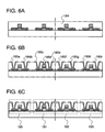
- an interlayer insulating film covering the semiconductor layers and the gate electrodes is formed.
- a single-layer structure of an interlayer insulating film 184 is shown.
- the interlayer insulating film 184 a silicon nitride film, a silicon nitride oxide film, a silicon oxynitride film, a silicon oxide film, or the like which can be formed by sputtering or plasma CVD may be used. Alternatively a stacked-layer structure of two or more layers may be used.
- heat treatment is performed at 300 to 550 °C for 1 to 12 hours in a nitrogen atmosphere to hydrogenate the semiconductor layers. This heat treatment is preferably performed at 400 to 500 °C. In this step, dangling bonds in the semiconductor layers are terminated by hydrogen contained in the interlayer insulating film 184. In this embodiment mode, heat treatment is performed at 410 °C for 1 hour.
- the interlayer insulating film 184 can be formed using a material selected from aluminum nitride, aluminum oxynitride, aluminum nitride oxide containing more nitrogen than oxygen, aluminum oxide, diamond-like carbon (DLC), nitrogen-containing carbon (CN), or any other substance containing an inorganic insulating material.
- a siloxane resin may be used.
- a siloxane resin is a resin containing a Si-O-Si bond.
- the skeleton structure of siloxane is formed of a bond of silicon and oxygen.
- an organic group containing at least hydrogen e.g., an alkyl group or aromatic hydrocarbon
- a fluoro group or a fluoro group and an organic group containing at least hydrogen may be used as the substituent.
- an organic insulating material may be used.
- an organic material polyimide, acrylic, polyamide, polyimide amide, resist, benzocyclobutene, polysilazane, or the like can be used.
- a coating film having favorable flatness, which is formed by a coating method, may be used.
- the interlayer insulating film 184 can be formed by dipping, spray coating, coating with a variety of coaters, an evaporation method, or the like, as well as sputtering or plasma CVD, which is described above.
- the interlayer insulating film 184 may be formed by a droplet discharge method. In this case, a material solution can be saved.
- a method by which a pattern can be transferred or drawn, like a droplet discharge method for example, a printing method (a method for forming a pattern, such as screen printing or offset printing), or the like can be used.
- contact holes opening portions which reach the semiconductor layer and the gate electrode layer are formed in the interlayer insulating film and the gate insulating film by using a mask formed of a resist.
- Etching may be performed only once or a plurality of times depending on selectivity of the materials which are used. Further, either wet etching or dry etching may be performed, or both wet etching and dry etching may be performed.
- a solution containing fluorinated acid such as a mixed solution containing ammonium hydrogen fluoride and ammonium fluoride.
- etching gas a chlorine-based gas typified by Cl 2 , BCl 3 , SiCl 4 , or CCl 4 ; a fluorine-based gas typified by CF 4 , SF 6 , or NF 3 ; or O 2 can be used as appropriate.
- an inert gas may be added to the etching gas.
- the inert gas element which is added one kind of element or a plurality of kinds of elements selected from He, Ne, Ar, Kr, or Xe can be used.
- a conductive film is formed so as to cover the opening portion, and the conductive film is etched to have a desired shape, so that wirings 185a to 185i which are electrically connected to part of a source region or a drain region, or a gate electrode are formed.
- the wirings 185a to 185i may be formed by forming a conductive layer as selected at a predetermined position by a droplet discharge method, a printing method, an electrolytic plating method, or the like.
- a reflow method or a damascene method may be used.
- the wirings 185a to 185i are formed using a metal such as Ag, Au, Cu, Ni, Pt, Pd, Ir, Rh, W, Al, Ta, Mo, Cd, Zn, Fe, Ti, Zr, or Ba; Si; Ge; or an alloy or metal nitride thereof.
- a stacked-layer structure of any of these materials may be used.
- a 60 nm-thick titanium (Ti) film, a 40 nm-titanium nitride film, a 700 nm-thick aluminum film, and a 200 nm-thick titanium (Ti) film are stacked and processed to have a desired shape (see FIG. 6B ).
- a semiconductor device which includes transistors 190 and 191 using semiconductor layers 151 and 152 as active layers, respectively, and transistors 192 and 193 using the single-crystal semiconductor layers 161 and 162 having compressive strain as active layers, respectively, over the same substrate (see FIG. 6C ).
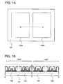
- FIGS. 1A and 1B show an example of a semiconductor device which is formed in accordance with this embodiment mode.
- FIG 1A is a plan view of a semiconductor device of the present invention
- FIG 1B is a cross-sectional view taken along X-Y in FIG. 1A .
- a first circuit group 1201 and a second circuit group 1202 are formed over the same base substrate 101.
- the first circuit group 1201 is formed using the transistors 190 and 191 which are formed using single-crystal semiconductor layers.
- the second circuit group 1202 is formed using the transistors 192 and 193 which are formed using single-crystal semiconductor layers having compressive strain.
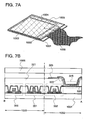
- FIGS. 7A and 7B an example of a semiconductor device having a display function, to which the present invention is applied, is described with reference to FIGS. 7A and 7B .
- FIG 7A shows an active matrix display device.
- a pixel portion 1002 where a plurality of pixel circuits are arranged in matrix, a data driver 1003, and a scan driver 1004 are formed over a base substrate 1001. Further, a top surface of the base substrate 1001 is hermetically sealed with a counter substrate (a sealing substrate) 1005.
- a control signal, an image signal, and driving power which are necessary for driving a display device are supplied from outside through a flexible printed circuit (FPC) 1006.
- FIG 7B is a cross-sectional view taken along A-B in FIG 7A .
- FIG. 7B shows a cross section of an active matrix display device when a pixel portion is formed using an electroluminescence (EL) element.
- EL electroluminescence
- the data driver 1003 and the scan driver 1004 each perform processing for inputting an image signal supplied from outside to each pixel in accordance with a control signal supplied from outside, and the data driver 1003 and the scan driver 1004 each needs relatively high-speed operations in a display device.
- the data driver 1003 and the scan driver 1004 are formed by using transistors 350 and 351 which are formed by using the single-crystal semiconductor layers, which are formed over the base substrate 1001 through the above-described process, as active layers.
- the transistors 350 and 351 have sufficient capability for driving the data driver 1003 and the scan driver 1004.
- a light-transmitting substrate formed using glass, plastic, or the like is preferably used as the base substrate 1001. Needless to say, a material which can withstand the heat treatment through the above-described step should be selected.
- the pixel portion 1002 is formed by using a transistor 352 which is formed by using the single-crystal semiconductor layer having compressive strain, which is formed over the base substrate 1001 through the above-described process, as an active layer.
- a p-channel transistor is used as the transistor 352. This is because supply of current to the EL element is continuously performed during a display period, that is, current is continuously supplied to the transistor, so that hot carrier deterioration or the like is concerned when an n-channel transistor is used.
- compressive strain is applied to the active layer of the p-channel transistor 352 included in the pixel portion, and mobility of holes is improved. Therefore, the p-channel transistor 352 can sufficiently supply current to the EL element even when the channel width is decreased.
- the arrangement area of the transistor 352 in the pixel portion can be relatively decreased and the aperture ratio (a ratio of a region which contributes to light emission to the whole area of the pixel portion) can be improved.
- Polarities of transistors which lead improvement in mobility are different between the case where tensile strain is applied to a semiconductor layer and the case where compressive strain is applied to a semiconductor layer. Specifically, in the case where tensile strain is applied to a semiconductor layer, electron mobility is improved in an n-channel transistor, and in the case where compressive strain is applied to a semiconductor layer, hole mobility is improved in a p-channel transistor.
- semiconductor device of the present invention in accordance with each characteristics of circuit groups, which semiconductor layer to be used to form a transistor for forming the circuit may be selected as appropriate.
- a scan driver and a data driver are illustrated as circuits provided around the pixel portion in this embodiment mode, another logic circuit may be formed at the same time.
- a first electrode layer 320 serving as a pixel electrode layer is formed to be in contact with an electrode of the transistor 352.
- the first electrode layer 320 can be formed using a light-transmitting conductive material such as indium tin oxide (ITO), indium tin oxide containing silicon oxide (TTSO), indium zinc oxide (IZO) containing zinc oxide (ZnO), zinc oxide, ZnO doped with gallium (Ga), tin oxide (SnO 2 ), indium oxide containing tungsten oxide, indium zinc oxide containing tungsten oxide, indium oxide containing titanium oxide, or indium tin oxide containing titanium oxide.
- ITO indium tin oxide
- TTSO indium tin oxide containing silicon oxide
- IZO indium zinc oxide
- ZnO zinc oxide
- Ga gallium
- SnO 2 tin oxide
- the film thickness is made extremely thin (preferably approximately 5 to 30 nm) so that light can be transmitted, light can be emitted through the first electrode layer 320.
- a metal thin film which can be used for the first electrode layer 320 a conductive film formed using titanium, tungsten, nickel, gold, platinum, silver, aluminum, magnesium, calcium, lithium, zinc, or alloy thereof, or a film formed using a compound material containing any of the above-described elements as a main component, such as titanium nitride or tungsten nitride can be used.
- connection structure of the first electrode layer 320 is not limited to that described in this embodiment mode as long as the first electrode layer 320 is electrically connected to a source electrode or drain electrode of the transistor 352.
- a structure may be employed in which an insulating layer serving as an interlayer insulating layer is formed over a source electrode or a drain electrode and is electrically connected to the first electrode layer 320 by a wiring layer.
- a metal material such as gold, silver, copper, tungsten, or aluminum can be used because the first electrode layer 320 does not need light-transmitting properties.
- an insulating layer 321 (also referred to as a partition) is formed as selected.
- the insulating layer 321 is formed so as to have an opening portion over the first electrode layer 320.
- the insulating layer 321 is processed by being etched by a mask such as a resist.
- a mask such as a resist.
- the insulating layer 321 can be formed using an inorganic insulating material such as silicon oxide, silicon nitride, silicon oxynitride, aluminum oxide, aluminum nitride, or aluminum oxynitride; an acrylic acid, a methacrylic acid, or a derivative thereof; a heat-resistant high molecule such as polyimide, aromatic polyamide, or polybenzimidazole; or a siloxane resin material.
- the insulating layer 321 preferably has a shape in which a radius of curvature changes continuously because coverage thereof with a light-emitting layer 322 and a second electrode layer 323 which are formed thereover is improved.
- materials emitting light of red (R), green (G), and blue (B) are formed as selected by an evaporation method or the like using evaporation masks.
- the materials emitting light of red (R), green (G), and blue (B) can be formed by a droplet discharge method.
- a laser transfer method may be used in which a substrate where the materials of respective colors are uniformly evaporated is prepared and provided so as to face with the base substrate 1001, and a light-emitting material is transferred to a desired position by laser irradiation or the like from the rear surface.
- the light-emitting material can be formed as selected at a desired position without using the evaporation masks
- a second electrode layer 323 is formed over the light-emitting layer 322, and the pixel portion is sealed with the counter substrate (sealing substrate) 1005. Therefore, a display device is completed.
- a passivation film which is provided when a display device is formed may have a single-layer structure or a stacked-layer structure.
- the passivation film is formed using an insulating film containing silicon nitride, silicon oxide, silicon oxynitride, silicon nitride oxide, aluminum nitride (AlN), aluminum oxynitride, aluminum nitride oxide containing more nitrogen than oxygen, aluminum oxide, diamond-like carbon, or nitrogen-containing carbon, and the insulating film can have a single-layer structure or a stacked-layer structure.
- a stacked-layer of a carbon-containing nitrogen film and a silicon nitride film or an organic material can be used, or a stacked-layer of a high molecular such as a styrene polymer may be used.
- a siloxane material inorganic siloxane or organic siloxane may be used.
- a film having favorable coverage as the passivation film it is preferable to use a film having favorable coverage as the passivation film, and it is effective to use a carbon film, particularly, a DLC film as the passivation film. Since a DLC film can be formed in the range from room temperature to 100 °C, it can also be formed easily over an electroluminescent layer with low heat resistance. A DLC film has a high blocking effect against oxygen, and oxidization of the electroluminescent layer can be suppressed. Accordingly, a problem such as oxidation of the electroluminescent layer during a sealing step which is subsequently performed can be solved.
- a space between the base substrate (insulating substrate) 1001 and the counter substrate (sealing substrate) 1005 is filled with a filler and can be sealed with a sealant.
- a dripping method can be used for filling the space with the filler.
- the space may be filled with an inert gas such as nitrogen.
- a drying agent is provided in the display device, deterioration due to moisture in the light-emitting element can be prevented.
- Sealing treatment corresponds to treatment for protecting a light-emitting element from moisture, and any of the following methods is used: a method of mechanically sealing with a cover material, a method of sealing with a thermosetting resin or an ultraviolet curable resin, and a method of sealing with a thin film having high barrier capability, which is formed using metal oxide, nitride, or the like.
- a cover material glass, ceramics, plastic, or metal can be used, and in the case where light is emitted on the cover material side, the cover material should have light-transmitting properties.
- the cover material and the substrate provided with the light-emitting element are attached with a sealant such as a thermosetting resin or an ultraviolet curable resin, and the resin is cured by heat treatment or ultraviolet irradiation treatment to form a hermetical space.
- a sealant such as a thermosetting resin or an ultraviolet curable resin
- the absorbent material may be provided to be in contact with the sealant, or may be provided over a partition or at a peripheral portion so as not to impede light from the light-emitting element.
- the space between the cover material and the substrate provided with the light-emitting element can be filled with a thermosetting resin or an ultraviolet curable resin. In this case, it is effective to add an absorbent material typified by barium oxide in the thermosetting resin or the ultraviolet curable resin.
- an EL element is used for a pixel portion as an example of a display device
- the present invention does not limit the type of a display device.
- a transistor formed using a single-crystal semiconductor layer and a transistor formed using a single-crystal semiconductor layer to which compressive strain is applied may be used for the peripheral circuit portion and the pixel portion, respectively, as appropriate.
- a transistor formed using a single-crystal semiconductor layer which is used for the peripheral circuit
- a transistor formed using a single-crystal semiconductor layer to which tensile strain is applied may be used.
- Embodiment Mode can be combined with Embodiment Mode 1 as appropriate.
- a thin single-crystal semiconductor layer 150 and a thick single-crystal semiconductor layer 160 are formed over the base substrate 101 by being attached thereto; however, there is the case where part of a separation plane due to an ion irradiation step is left remaining on an outermost surface of each single-crystal semiconductor layer. Since the separation plane is a region which is in contact with a region where the weakened layer (the separation layer) is formed by hydrogen ion irradiation, the separation plane has flatness inferior to the surface of a normal single-crystal semiconductor layer. Therefore, it is necessary to improve the surface condition of the separation plane in order to prevent defects in subsequent steps.
- CMP chemical mechanical polishing
- the separation plane is oxidized by surface oxidation and then the oxidized layer is removed in a reducing atmosphere, for example.
- the surface may be improved by any one of methods.
- Embodiment Mode 1 or 2 can be combined with Embodiment Mode 1 or 2 as appropriate.
- a semiconductor device having a variety of display functions can be manufactured. That is, the present invention can be applied to a variety of electronic devices in which a semiconductor device having such display functions is incorporated in a display portion.
- examples of electronic devices which include a semiconductor device having a display function, which aims at high performance and high reliability, are shown.
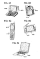
- Examples of electronic devices of the present invention are a television set (also simply referred to as a television or a television receiver), a camera such as a digital camera or a digital video camera, a portable phone device (also simply referred to as a portable phone), a portable information terminal such as a PDA, a portable game machine, a computer monitor, a computer, an audio reproducing device such as a car audio component, an image reproducing device provided with a recording medium, such as a home-use game machine (e.g., a device which reproduces a digital versatile disc (DVD)), and the like. Specific examples thereof are described with reference to FIGS. 8A to 8E .
- a portable information terminal shown in FIG 8A includes a main body 9201, a display portion 9202, and the like.
- the semiconductor device of the present invention can be applied to the display portion 9202.
- a digital video camera shown in FIG. 8B includes a display portion 9701, a display portion 9702, and the like.
- the semiconductor device of the present invention can be applied to the display portion 9701.
- a mobile phone shown in FIG 8C includes a main body 9101, a display portion 9102, and the like.
- the semiconductor device of the present invention can be applied to the display portion 9102.
- a portable television set shown in FIG 8D includes a main body 9301, a display portion 9302, and the like.
- the semiconductor device of the present invention can be applied to the display portion 9302. Further, the semiconductor device of the present invention can be applied to a wide range of television sets ranging from a small-sized television set mounted on a portable terminal such as a mobile phone, a medium-sized television set which can be carried, to a large-sized (e.g., 40-inch or larger) television set.
- a portable computer shown in FIG. 8E includes a main body 9401, a display portion 9402, and the like.
- the semiconductor device of the present invention can be applied to the display portion 9402.
- Embodiment Mode can be combined with Embodiment Modes 1 to 3 as appropriate.
- a television set can be completed using a semiconductor device including a display element formed by the present invention.
- An example of a television set which has high performance and high reliability is described.
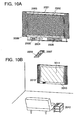
- FIG. 9 is a block diagram showing a main structure of a television set (a liquid crystal television set, an EL television set, or the like).
- a display panel can be formed in any mode as follows: a mode in which a TFT is formed, and a pixel region 1901 and a scan line driver circuit 1903 are formed over the same substrate, and a signal line driver circuit 1902 is separately mounted as a driver IC; a mode in which the pixel region 1901, the signal line driver circuit 1902, and the scan line driver circuit 1903 are formed over the same substrate; and the like.
- a video signal amplifier circuit 1905 amplifying a video signal among signals received by a tuner 1904, a video signal processing circuit 1906 converting signals output from the video signal amplifier circuit 1905 into chrominance signals corresponding to respective colors of red, green, and blue, a control circuit 1907 for converting the video signal into a signal which meets input specifications of a driver IC, and the like are provided on an input side of the video signal.
- the control circuit 1907 outputs signals to both a scan line side and a signal line side.
- a signal dividing circuit 1908 may be provided on the signal line side and an input digital signal may be divided into m pieces to be supplied.
- an audio signal is transmitted to an audio signal amplifier circuit 1909, and output thereof is supplied to a speaker 1913 through an audio signal processing circuit 1910.
- a control circuit 1911 receives control information on a receiving station (receiving frequency) or sound volume from an input portion 1912 and transmits the signal to the tuner 1904 or the audio signal processing circuit 1910.
- a television set can be completed when a display module is incorporated in a housing, as shown in FIGS. 10A and 10B .
- a display panel as shown in FIGS. 7A and 7B , on which an FPC is mounted, is also referred to as an EL display module generally.
- an EL display module as shown in FIGS. 7A and 7B is used, an EL television set can be completed.
- a liquid crystal display module is used, a liquid crystal television set can be completed.
- a main screen 2003 is formed using the display module, and a speaker portion 2009, operation switches, and the like are provided as its accessory equipment.
- a television set can be completed by the present invention.
- reflected incident light from outside may be blocked by using a retardation plate or a polarizing plate.
- an insulating layer serving as a partition may be colored to be used as a black matrix.
- This partition can also be formed by a droplet discharge method or the like. Carbon black or the like may be mixed into a black resin of a pigment material or a resin material such as polyimide, or a laminate thereof may be used. By a droplet discharge method, different materials may be discharged to the same region plural times to form the partition.
- a ⁇ /4 plate or a ⁇ /2 plate may be used as the retardation plate and may be designed so that light can be controlled.
- a light-emitting element, a sealing substrate (a sealant), the retardation plates (a ⁇ /4 plate and a ⁇ /2 plate), and the polarizing plate are sequentially formed in that order from the TFT element substrate side, and light emitted from the light-emitting element is transmitted therethrough and is emitted outside from the polarizing plate side.
- the retardation plate or the polarizing plate may be provided on a side to which light is emitted or can be provided on both sides in the case of a dual-emission semiconductor device in which light is emitted across the both sides.
- an antireflective film may be provided on the outer side of the polarizing plate.
- a display panel 2002 using a display element is incorporated in a housing 2001.
- a receiver 2005 including reception of general TV broadcast, communication of information can also be performed in one way (from a transmitter to a receiver) or in two ways (between a transmitter and a receiver or between receivers) by connection to a wired or wireless communication network through a modem 2004.
- the television set can be operated by switches incorporated in the housing or by a remote controller 2006 separated from the main body.
- a display portion 2007 displaying information to be output may also be provided in this remote controller.
- a structure for displaying a channel, sound volume, or the like may be added by forming a subscreen 2008 with a second display panel in addition to the main screen 2003.
- the main screen 2003 may be formed using an EL display panel superior in the viewing angle
- the subscreen 2008 may be formed using a liquid crystal display panel capable of displaying images with low power consumption.
- a structure in which the main screen 2003 is formed using a liquid crystal display panel, the subscreen 2008 is formed using an EL display panel, and the subscreen 2008 can flash on and off may be employed.
- a display device which has high performance and high reliability can be manufactured with high productivity even when such a large substrate and many TFTs and electronic components are used.
- FIG 10B shows a television set having a large display portion, for example, 20 to 80-inch display portion, which includes a housing 2010, a display portion 2011, a remote controller 2012 which is an operation portion, a speaker portion 2013, and the like.
- the present invention is applied to manufacture of the display portion 2011.
- the television set shown in FIG. 10B is a wall-hanging type and does not need a wide space.
- the present invention is not limited to the television set, and can be applied to various uses particularly as a large display medium such as an information display board at a train station, an airport, or the like, or an advertisement display board on the street, as well as a monitor of a personal computer.
- Embodiment Mode can be combined with Embodiment Modes 1 to 4 as appropriate.
- This application is based on Japanese Patent Application serial no. 2007-173452 filed with Japan Patent Office on June 29, 2007, the entire contents of which are hereby incorporated by reference.
Landscapes
- Thin Film Transistor (AREA)
- Liquid Crystal (AREA)
- Electroluminescent Light Sources (AREA)
- Metal-Oxide And Bipolar Metal-Oxide Semiconductor Integrated Circuits (AREA)
- Recrystallisation Techniques (AREA)
- Element Separation (AREA)
Applications Claiming Priority (1)
| Application Number | Priority Date | Filing Date | Title |
|---|---|---|---|
| JP2007173452 | 2007-06-29 |
Publications (2)
| Publication Number | Publication Date |
|---|---|
| EP2009694A2 true EP2009694A2 (de) | 2008-12-31 |
| EP2009694A3 EP2009694A3 (de) | 2017-06-21 |
Family
ID=39791344
Family Applications (1)
| Application Number | Title | Priority Date | Filing Date |
|---|---|---|---|
| EP08010529.9A Withdrawn EP2009694A3 (de) | 2007-06-29 | 2008-06-10 | Halbleiterbauelement und Herstellungsverfahren dafür |
Country Status (4)
| Country | Link |
|---|---|
| US (2) | US7915684B2 (de) |
| EP (1) | EP2009694A3 (de) |
| JP (1) | JP5325477B2 (de) |
| KR (1) | KR101510687B1 (de) |
Families Citing this family (4)
| Publication number | Priority date | Publication date | Assignee | Title |
|---|---|---|---|---|
| KR20120058106A (ko) * | 2010-11-29 | 2012-06-07 | 삼성전자주식회사 | 액정 표시 장치 및 그 제조 방법 |
| TWI755773B (zh) | 2014-06-30 | 2022-02-21 | 日商半導體能源研究所股份有限公司 | 發光裝置,模組,及電子裝置 |
| US10516075B2 (en) | 2017-09-11 | 2019-12-24 | Nichia Corporation | Method of manufacturing a light emitting element |
| JPWO2021090106A1 (de) * | 2019-11-08 | 2021-05-14 |
Citations (3)
| Publication number | Priority date | Publication date | Assignee | Title |
|---|---|---|---|---|
| JPH11163363A (ja) | 1997-11-22 | 1999-06-18 | Semiconductor Energy Lab Co Ltd | 半導体装置およびその作製方法 |
| JP2000124092A (ja) | 1998-10-16 | 2000-04-28 | Shin Etsu Handotai Co Ltd | 水素イオン注入剥離法によってsoiウエーハを製造する方法およびこの方法で製造されたsoiウエーハ |
| JP2007173452A (ja) | 2005-12-21 | 2007-07-05 | Matsushita Electric Ind Co Ltd | バイポーラトランジスタおよびその製造方法 |
Family Cites Families (21)
| Publication number | Priority date | Publication date | Assignee | Title |
|---|---|---|---|---|
| KR0143873B1 (ko) * | 1993-02-19 | 1998-08-17 | 순페이 야마자끼 | 절연막 및 반도체장치 및 반도체 장치 제조방법 |
| JPH09116167A (ja) * | 1994-12-27 | 1997-05-02 | Seiko Epson Corp | 薄膜半導体装置、液晶表示装置及びその製造方法、並びに電子機器 |
| JP3372158B2 (ja) | 1996-02-09 | 2003-01-27 | 株式会社東芝 | 半導体装置及びその製造方法 |
| JPH11145438A (ja) * | 1997-11-13 | 1999-05-28 | Shin Etsu Handotai Co Ltd | Soiウエーハの製造方法ならびにこの方法で製造されるsoiウエーハ |
| JP2000012864A (ja) | 1998-06-22 | 2000-01-14 | Semiconductor Energy Lab Co Ltd | 半導体装置の作製方法 |
| US6271101B1 (en) | 1998-07-29 | 2001-08-07 | Semiconductor Energy Laboratory Co., Ltd. | Process for production of SOI substrate and process for production of semiconductor device |
| JP4476390B2 (ja) | 1998-09-04 | 2010-06-09 | 株式会社半導体エネルギー研究所 | 半導体装置の作製方法 |
| US6420758B1 (en) * | 1998-11-17 | 2002-07-16 | Semiconductor Energy Laboratory Co., Ltd. | Semiconductor device having an impurity region overlapping a gate electrode |
| TW511298B (en) * | 1999-12-15 | 2002-11-21 | Semiconductor Energy Lab | EL display device |
| SG114530A1 (en) | 2001-02-28 | 2005-09-28 | Semiconductor Energy Lab | Method of manufacturing a semiconductor device |
| JP4831885B2 (ja) | 2001-04-27 | 2011-12-07 | 株式会社半導体エネルギー研究所 | 半導体装置の作製方法 |
| JP3913534B2 (ja) * | 2001-11-30 | 2007-05-09 | 株式会社半導体エネルギー研究所 | 表示装置及びこれを用いた表示システム |
| WO2003105204A2 (en) * | 2002-06-07 | 2003-12-18 | Amberwave Systems Corporation | Semiconductor devices having strained dual channel layers |
| JP2004281878A (ja) * | 2003-03-18 | 2004-10-07 | Seiko Epson Corp | 半導体基板の製造方法及びこれにより製造される半導体基板、電気光学装置並びに電子機器 |
| KR100483049B1 (ko) * | 2003-06-03 | 2005-04-15 | 삼성전기주식회사 | 수직구조 질화갈륨계 발광다이오드의 제조방법 |
| US6852652B1 (en) * | 2003-09-29 | 2005-02-08 | Sharp Laboratories Of America, Inc. | Method of making relaxed silicon-germanium on glass via layer transfer |
| CN101091251B (zh) * | 2004-08-18 | 2011-03-16 | 康宁股份有限公司 | 包含高应变玻璃或玻璃陶瓷的绝缘体上半导体结构 |
| US7393733B2 (en) * | 2004-12-01 | 2008-07-01 | Amberwave Systems Corporation | Methods of forming hybrid fin field-effect transistor structures |
| JP4942341B2 (ja) * | 2004-12-24 | 2012-05-30 | 三洋電機株式会社 | 表示装置 |
| US7470573B2 (en) * | 2005-02-18 | 2008-12-30 | Sharp Laboratories Of America, Inc. | Method of making CMOS devices on strained silicon on glass |
| JP2006324426A (ja) * | 2005-05-18 | 2006-11-30 | Sony Corp | 半導体装置およびその製造方法 |
-
2008
- 2008-06-10 EP EP08010529.9A patent/EP2009694A3/de not_active Withdrawn
- 2008-06-11 US US12/136,875 patent/US7915684B2/en not_active Expired - Fee Related
- 2008-06-25 KR KR20080060103A patent/KR101510687B1/ko not_active Expired - Fee Related
- 2008-06-27 JP JP2008168824A patent/JP5325477B2/ja not_active Expired - Fee Related
-
2011
- 2011-02-10 US US13/024,808 patent/US8324077B2/en not_active Expired - Fee Related
Patent Citations (3)
| Publication number | Priority date | Publication date | Assignee | Title |
|---|---|---|---|---|
| JPH11163363A (ja) | 1997-11-22 | 1999-06-18 | Semiconductor Energy Lab Co Ltd | 半導体装置およびその作製方法 |
| JP2000124092A (ja) | 1998-10-16 | 2000-04-28 | Shin Etsu Handotai Co Ltd | 水素イオン注入剥離法によってsoiウエーハを製造する方法およびこの方法で製造されたsoiウエーハ |
| JP2007173452A (ja) | 2005-12-21 | 2007-07-05 | Matsushita Electric Ind Co Ltd | バイポーラトランジスタおよびその製造方法 |
Non-Patent Citations (2)
| Title |
|---|
| IEDM TECH. DIGEST, 1994, pages 373 - 376 |
| IEEE ELECTRON DEVICE LETTERS, vol. 15, no. 10, 1994, pages 402 - 405 |
Also Published As
| Publication number | Publication date |
|---|---|
| US7915684B2 (en) | 2011-03-29 |
| JP2009033144A (ja) | 2009-02-12 |
| KR101510687B1 (ko) | 2015-04-10 |
| EP2009694A3 (de) | 2017-06-21 |
| KR20090004549A (ko) | 2009-01-12 |
| US20110129987A1 (en) | 2011-06-02 |
| US8324077B2 (en) | 2012-12-04 |
| US20090002589A1 (en) | 2009-01-01 |
| JP5325477B2 (ja) | 2013-10-23 |
Similar Documents
| Publication | Publication Date | Title |
|---|---|---|
| US7750345B2 (en) | Semiconductor device | |
| JP5322467B2 (ja) | 表示装置の製造方法及びトランジスタを含む回路の製造方法 | |
| US8003483B2 (en) | Method for manufacturing SOI substrate | |
| US7520790B2 (en) | Display device and manufacturing method of display device | |
| US7737449B2 (en) | Light emitting device and method of manufacturing thereof | |
| US7994022B2 (en) | Semiconductor substrate and semiconductor device and manufacturing method of the same | |
| US7144819B2 (en) | Method for manufacturing a semiconductor device | |
| US8318587B2 (en) | Method for manufacturing semiconductor device | |
| JP2009027150A (ja) | 半導体装置製造用基板及びその作製方法 | |
| US8216914B2 (en) | Method for manufacturing SOI substrate and method for manufacturing semiconductor device | |
| US8324077B2 (en) | Semiconductor device and manufacturing method thereof | |
| US8518797B2 (en) | Method of making an SOI substrate by using a separation layer with regions of non-uniform concentration | |
| US8324084B2 (en) | Manufacturing method of semiconductor substrate and manufacturing method of semiconductor device | |
| JP2003163194A (ja) | 研磨方法及び半導体装置の作製方法 |
Legal Events
| Date | Code | Title | Description |
|---|---|---|---|
| PUAI | Public reference made under article 153(3) epc to a published international application that has entered the european phase |
Free format text: ORIGINAL CODE: 0009012 |
|
| AK | Designated contracting states |
Kind code of ref document: A2 Designated state(s): AT BE BG CH CY CZ DE DK EE ES FI FR GB GR HR HU IE IS IT LI LT LU LV MC MT NL NO PL PT RO SE SI SK TR |
|
| AX | Request for extension of the european patent |
Extension state: AL BA MK RS |
|
| PUAL | Search report despatched |
Free format text: ORIGINAL CODE: 0009013 |
|
| AK | Designated contracting states |
Kind code of ref document: A3 Designated state(s): AT BE BG CH CY CZ DE DK EE ES FI FR GB GR HR HU IE IS IT LI LT LU LV MC MT NL NO PL PT RO SE SI SK TR |
|
| AX | Request for extension of the european patent |
Extension state: AL BA MK RS |
|
| RIC1 | Information provided on ipc code assigned before grant |
Ipc: H01L 29/78 20060101ALI20170512BHEP Ipc: H01L 21/77 20170101ALI20170512BHEP Ipc: H01L 27/12 20060101AFI20170512BHEP Ipc: H01L 29/786 20060101ALI20170512BHEP |
|
| REG | Reference to a national code |
Ref country code: DE Ref legal event code: R108 |
|
| AKY | No designation fees paid | ||
| AXX | Extension fees paid |
Extension state: RS Extension state: MK Extension state: BA Extension state: AL |
|
| STAA | Information on the status of an ep patent application or granted ep patent |
Free format text: STATUS: THE APPLICATION IS DEEMED TO BE WITHDRAWN |
|
| 18D | Application deemed to be withdrawn |
Effective date: 20171222 |