EP2009714A2 - Dispositif et procédé de séparation, en particulier de couches dotées à l'aide d'OVPD ou analogues - Google Patents
Dispositif et procédé de séparation, en particulier de couches dotées à l'aide d'OVPD ou analogues Download PDFInfo
- Publication number
- EP2009714A2 EP2009714A2 EP08159270A EP08159270A EP2009714A2 EP 2009714 A2 EP2009714 A2 EP 2009714A2 EP 08159270 A EP08159270 A EP 08159270A EP 08159270 A EP08159270 A EP 08159270A EP 2009714 A2 EP2009714 A2 EP 2009714A2
- Authority
- EP
- European Patent Office
- Prior art keywords
- modification
- starting material
- dopant
- chamber
- plasma
- Prior art date
- Legal status (The legal status is an assumption and is not a legal conclusion. Google has not performed a legal analysis and makes no representation as to the accuracy of the status listed.)
- Granted
Links
Images
Classifications
-
- C—CHEMISTRY; METALLURGY
- C23—COATING METALLIC MATERIAL; COATING MATERIAL WITH METALLIC MATERIAL; CHEMICAL SURFACE TREATMENT; DIFFUSION TREATMENT OF METALLIC MATERIAL; COATING BY VACUUM EVAPORATION, BY SPUTTERING, BY ION IMPLANTATION OR BY CHEMICAL VAPOUR DEPOSITION, IN GENERAL; INHIBITING CORROSION OF METALLIC MATERIAL OR INCRUSTATION IN GENERAL
- C23C—COATING METALLIC MATERIAL; COATING MATERIAL WITH METALLIC MATERIAL; SURFACE TREATMENT OF METALLIC MATERIAL BY DIFFUSION INTO THE SURFACE, BY CHEMICAL CONVERSION OR SUBSTITUTION; COATING BY VACUUM EVAPORATION, BY SPUTTERING, BY ION IMPLANTATION OR BY CHEMICAL VAPOUR DEPOSITION, IN GENERAL
- C23C14/00—Coating by vacuum evaporation, by sputtering or by ion implantation of the coating forming material
- C23C14/06—Coating by vacuum evaporation, by sputtering or by ion implantation of the coating forming material characterised by the coating material
- C23C14/12—Organic material
-
- B—PERFORMING OPERATIONS; TRANSPORTING
- B82—NANOTECHNOLOGY
- B82Y—SPECIFIC USES OR APPLICATIONS OF NANOSTRUCTURES; MEASUREMENT OR ANALYSIS OF NANOSTRUCTURES; MANUFACTURE OR TREATMENT OF NANOSTRUCTURES
- B82Y10/00—Nanotechnology for information processing, storage or transmission, e.g. quantum computing or single electron logic
-
- C—CHEMISTRY; METALLURGY
- C23—COATING METALLIC MATERIAL; COATING MATERIAL WITH METALLIC MATERIAL; CHEMICAL SURFACE TREATMENT; DIFFUSION TREATMENT OF METALLIC MATERIAL; COATING BY VACUUM EVAPORATION, BY SPUTTERING, BY ION IMPLANTATION OR BY CHEMICAL VAPOUR DEPOSITION, IN GENERAL; INHIBITING CORROSION OF METALLIC MATERIAL OR INCRUSTATION IN GENERAL
- C23C—COATING METALLIC MATERIAL; COATING MATERIAL WITH METALLIC MATERIAL; SURFACE TREATMENT OF METALLIC MATERIAL BY DIFFUSION INTO THE SURFACE, BY CHEMICAL CONVERSION OR SUBSTITUTION; COATING BY VACUUM EVAPORATION, BY SPUTTERING, BY ION IMPLANTATION OR BY CHEMICAL VAPOUR DEPOSITION, IN GENERAL
- C23C14/00—Coating by vacuum evaporation, by sputtering or by ion implantation of the coating forming material
- C23C14/22—Coating by vacuum evaporation, by sputtering or by ion implantation of the coating forming material characterised by the process of coating
- C23C14/228—Gas flow assisted PVD deposition
-
- C—CHEMISTRY; METALLURGY
- C23—COATING METALLIC MATERIAL; COATING MATERIAL WITH METALLIC MATERIAL; CHEMICAL SURFACE TREATMENT; DIFFUSION TREATMENT OF METALLIC MATERIAL; COATING BY VACUUM EVAPORATION, BY SPUTTERING, BY ION IMPLANTATION OR BY CHEMICAL VAPOUR DEPOSITION, IN GENERAL; INHIBITING CORROSION OF METALLIC MATERIAL OR INCRUSTATION IN GENERAL
- C23C—COATING METALLIC MATERIAL; COATING MATERIAL WITH METALLIC MATERIAL; SURFACE TREATMENT OF METALLIC MATERIAL BY DIFFUSION INTO THE SURFACE, BY CHEMICAL CONVERSION OR SUBSTITUTION; COATING BY VACUUM EVAPORATION, BY SPUTTERING, BY ION IMPLANTATION OR BY CHEMICAL VAPOUR DEPOSITION, IN GENERAL
- C23C14/00—Coating by vacuum evaporation, by sputtering or by ion implantation of the coating forming material
- C23C14/22—Coating by vacuum evaporation, by sputtering or by ion implantation of the coating forming material characterised by the process of coating
- C23C14/24—Vacuum evaporation
- C23C14/32—Vacuum evaporation by explosion; by evaporation and subsequent ionisation of the vapours, e.g. ion-plating
-
- H—ELECTRICITY
- H10—SEMICONDUCTOR DEVICES; ELECTRIC SOLID-STATE DEVICES NOT OTHERWISE PROVIDED FOR
- H10K—ORGANIC ELECTRIC SOLID-STATE DEVICES
- H10K50/00—Organic light-emitting devices
- H10K50/10—OLEDs or polymer light-emitting diodes [PLED]
-
- H—ELECTRICITY
- H10—SEMICONDUCTOR DEVICES; ELECTRIC SOLID-STATE DEVICES NOT OTHERWISE PROVIDED FOR
- H10K—ORGANIC ELECTRIC SOLID-STATE DEVICES
- H10K71/00—Manufacture or treatment specially adapted for the organic devices covered by this subclass
- H10K71/10—Deposition of organic active material
- H10K71/16—Deposition of organic active material using physical vapour deposition [PVD], e.g. vacuum deposition or sputtering
-
- H—ELECTRICITY
- H10—SEMICONDUCTOR DEVICES; ELECTRIC SOLID-STATE DEVICES NOT OTHERWISE PROVIDED FOR
- H10K—ORGANIC ELECTRIC SOLID-STATE DEVICES
- H10K71/00—Manufacture or treatment specially adapted for the organic devices covered by this subclass
- H10K71/30—Doping active layers, e.g. electron transporting layers
-
- B—PERFORMING OPERATIONS; TRANSPORTING
- B05—SPRAYING OR ATOMISING IN GENERAL; APPLYING FLUENT MATERIALS TO SURFACES, IN GENERAL
- B05D—PROCESSES FOR APPLYING FLUENT MATERIALS TO SURFACES, IN GENERAL
- B05D1/00—Processes for applying liquids or other fluent materials
- B05D1/60—Deposition of organic layers from vapour phase
-
- B—PERFORMING OPERATIONS; TRANSPORTING
- B05—SPRAYING OR ATOMISING IN GENERAL; APPLYING FLUENT MATERIALS TO SURFACES, IN GENERAL
- B05D—PROCESSES FOR APPLYING FLUENT MATERIALS TO SURFACES, IN GENERAL
- B05D1/00—Processes for applying liquids or other fluent materials
- B05D1/62—Plasma-deposition of organic layers
-
- H—ELECTRICITY
- H10—SEMICONDUCTOR DEVICES; ELECTRIC SOLID-STATE DEVICES NOT OTHERWISE PROVIDED FOR
- H10K—ORGANIC ELECTRIC SOLID-STATE DEVICES
- H10K10/00—Organic devices specially adapted for rectifying, amplifying, oscillating or switching; Organic capacitors or resistors having potential barriers
- H10K10/40—Organic transistors
- H10K10/46—Field-effect transistors, e.g. organic thin-film transistors [OTFT]
- H10K10/462—Insulated gate field-effect transistors [IGFETs]
- H10K10/484—Insulated gate field-effect transistors [IGFETs] characterised by the channel regions
-
- H—ELECTRICITY
- H10—SEMICONDUCTOR DEVICES; ELECTRIC SOLID-STATE DEVICES NOT OTHERWISE PROVIDED FOR
- H10K—ORGANIC ELECTRIC SOLID-STATE DEVICES
- H10K50/00—Organic light-emitting devices
- H10K50/10—OLEDs or polymer light-emitting diodes [PLED]
- H10K50/14—Carrier transporting layers
- H10K50/15—Hole transporting layers
- H10K50/155—Hole transporting layers comprising dopants
-
- H—ELECTRICITY
- H10—SEMICONDUCTOR DEVICES; ELECTRIC SOLID-STATE DEVICES NOT OTHERWISE PROVIDED FOR
- H10K—ORGANIC ELECTRIC SOLID-STATE DEVICES
- H10K50/00—Organic light-emitting devices
- H10K50/10—OLEDs or polymer light-emitting diodes [PLED]
- H10K50/14—Carrier transporting layers
- H10K50/16—Electron transporting layers
- H10K50/165—Electron transporting layers comprising dopants
-
- H—ELECTRICITY
- H10—SEMICONDUCTOR DEVICES; ELECTRIC SOLID-STATE DEVICES NOT OTHERWISE PROVIDED FOR
- H10K—ORGANIC ELECTRIC SOLID-STATE DEVICES
- H10K85/00—Organic materials used in the body or electrodes of devices covered by this subclass
- H10K85/20—Carbon compounds, e.g. carbon nanotubes or fullerenes
- H10K85/211—Fullerenes, e.g. C60
-
- H—ELECTRICITY
- H10—SEMICONDUCTOR DEVICES; ELECTRIC SOLID-STATE DEVICES NOT OTHERWISE PROVIDED FOR
- H10K—ORGANIC ELECTRIC SOLID-STATE DEVICES
- H10K85/00—Organic materials used in the body or electrodes of devices covered by this subclass
- H10K85/30—Coordination compounds
- H10K85/321—Metal complexes comprising a group IIIA element, e.g. Tris (8-hydroxyquinoline) gallium [Gaq3]
- H10K85/324—Metal complexes comprising a group IIIA element, e.g. Tris (8-hydroxyquinoline) gallium [Gaq3] comprising aluminium, e.g. Alq3
-
- H—ELECTRICITY
- H10—SEMICONDUCTOR DEVICES; ELECTRIC SOLID-STATE DEVICES NOT OTHERWISE PROVIDED FOR
- H10K—ORGANIC ELECTRIC SOLID-STATE DEVICES
- H10K85/00—Organic materials used in the body or electrodes of devices covered by this subclass
- H10K85/30—Coordination compounds
- H10K85/371—Metal complexes comprising a group IB metal element, e.g. comprising copper, gold or silver
-
- H—ELECTRICITY
- H10—SEMICONDUCTOR DEVICES; ELECTRIC SOLID-STATE DEVICES NOT OTHERWISE PROVIDED FOR
- H10K—ORGANIC ELECTRIC SOLID-STATE DEVICES
- H10K85/00—Organic materials used in the body or electrodes of devices covered by this subclass
- H10K85/60—Organic compounds having low molecular weight
- H10K85/631—Amine compounds having at least two aryl rest on at least one amine-nitrogen atom, e.g. triphenylamine
- H10K85/633—Amine compounds having at least two aryl rest on at least one amine-nitrogen atom, e.g. triphenylamine comprising polycyclic condensed aromatic hydrocarbons as substituents on the nitrogen atom
-
- Y—GENERAL TAGGING OF NEW TECHNOLOGICAL DEVELOPMENTS; GENERAL TAGGING OF CROSS-SECTIONAL TECHNOLOGIES SPANNING OVER SEVERAL SECTIONS OF THE IPC; TECHNICAL SUBJECTS COVERED BY FORMER USPC CROSS-REFERENCE ART COLLECTIONS [XRACs] AND DIGESTS
- Y02—TECHNOLOGIES OR APPLICATIONS FOR MITIGATION OR ADAPTATION AGAINST CLIMATE CHANGE
- Y02E—REDUCTION OF GREENHOUSE GAS [GHG] EMISSIONS, RELATED TO ENERGY GENERATION, TRANSMISSION OR DISTRIBUTION
- Y02E10/00—Energy generation through renewable energy sources
- Y02E10/50—Photovoltaic [PV] energy
- Y02E10/549—Organic PV cells
Definitions
- the invention relates to a method for producing in particular doped layers for electronic, luminescent or photovoltaic components, in particular OLEDs, wherein one or more liquid or solid starting materials are vaporized in a source or admixed as aerosol to a carrier gas and transported in this form into a deposition chamber, where they condense a preferably doped matrix forming on a substrate, in particular as a result of a temperature gradient.
- the invention further relates to a device for performing the method, comprising the sources and the sources with the deposition chamber connecting gas supply lines and arranged in the deposition chamber susceptor for receiving the substrate.
- OLEDs organic light emitting devices
- VTE vacuum thermal evaporation
- the generally liquid or solid starting materials are converted into so-called sources in the OVPD process, for example, by evaporation into a gaseous form and then preferably transported by using a carrier gas through gas lines in a deposition chamber.
- the light-emitting diodes (OLEDs) produced from these layers generate light when current flows through.
- the flow of current is effected by electron conduction or by hole conduction, the current density not only depending on the hole concentration or the electron concentration, but also on their mobility. At present, it is possible to produce OLEDs with an efficiency of 20 lm / W.
- the deposited layers are electrically doped. It is also known in the prior art to produce stacked OLEDs by depositing different or identical OLED stacks with doped intermediate layers on one another. In addition to light emitting diodes and solar cells are manufactured with the described method. These photovoltaic devices also require high conductivity.
- an optical doping of the layers can also be carried out.
- the charge carriers In contrast to inorganic semiconductors, in which it is possible to introduce states in the band gap by targeted doping, in organic layers the charge carriers must be located on an organic molecule. If a dopant is used in addition to the matrix material forming starting materials, a chemical reaction (REDOX) between dopant and matrix material is required. This chemical reaction changes the organic molecule itself, creating new states / bonding conditions. The latter must take place because of the instability of the molecules used below 200 ° C and especially at room temperature.
- REDOX chemical reaction
- From the DE 10338406 A1 is a method known to be doped with the organic semiconductor materials with increased carrier density.
- the doping is carried out by mixing a neutral organic compound in the matrix.
- the organic compound is present in a hydrogenated form. It is mixed directly into the organic semiconductor material. They are nonionic molecules. They therefore show a substantially complete sublimation.
- the uncharged organic compound is converted into a cation or a radical by elimination of hydrogen.
- an electron from the radical to the semiconductor material an n-doping or by incorporating an electron through the cation from the semiconductor material, a p-doping.
- the DD 279032 A1 describes a method for producing organic semiconductor layers.
- thin layers are deposited on substrates.
- a solid stoichiometric 1: 1 complex of a donor is mixed with an acceptor and a solid acceptor in a predetermined non-integer ratio.
- the evaporated materials deposit on the substrate as a layer.
- the US Pat. No. 7,201,942 B2 describes an apparatus and method for performing conventional OVPD. Above a process chamber several liquid sources are arranged, which contain starting materials which are introduced in the gas phase transport into the process chamber.
- the US 6,207,238 B1 describes the deposition of a polymeric layer wherein the polymers are pretreated in a high vacuum process by means of a plasma.
- the invention has for its object to provide measures by which the doping of electronic, luminescent or photovoltaic layers is improved.
- the method is further developed such that the dopant or the doping are formed by modification of a starting material on its transport path.
- the modification does not take place in the already deposited layer, but away from the substrate in the gas phase.
- the modification takes place spatially between the source and the substrate in a gas phase, ie after evaporation in the gas phase.
- a neutral starting material which would lead to no doping without modification, is modified in time during the gas phase transport, ie in the gaseous state of the starting material and in the presence of a carrier gas.
- the modification of the starting material may take place in a modification chamber located downstream of the source and upstream of the deposition chamber.
- the modification is a change of the starting material.
- the starting material can be changed chemically or physically.
- the modification can be a matter transformation.
- the starting material can be broken down into several products.
- the modification can be both an analysis and a synthesis. The latter is achieved, for example, by reacting the starting material with a reaction partner.
- the starting material can react chemically with a reaction partner.
- the doping may be achieved by suitably chemically converting a starting material so that the layer formed using this starting material acquires higher electrical conductivity or other optical property.
- the modification can also be caused by merely supplying energy.
- the energy can be supplied by way of a plasma to the starting material. But it is also possible to add the energy by means of a high-frequency generator to the starting material. The use of heat and a heat-generating heating is also considered.
- the doping of the layer is caused by the fact that likewise a starting material is modified, so that the electron density or the hole density in the deposited layer increases or the optical properties of the deposited layer change. It can only be an energetic stimulus here.
- a starting material which forms the dopant that is to say a precursor of the dopant, is modified.
- the precursor of the dopant itself may not be able to be incorporated into the matrix while increasing conductivity. Rather, the precursor of the precursor must then first be modified in the aforementioned manner to produce a dopant that can be incorporated into the matrix.
- the dopant is produced by modification of a starting material
- the starting material would form a non-conductive or poorly conductive layer without modification in the layer. He gets by the modification of a dopant property. If this modified starting material is incorporated into the matrix, the electrical conductivity is increased.
- the modification can be done by energy, by synthesis or analysis.
- ions or neutral radicals can be formed. These ions or neutral radicals can unfold the dopant function. They are introduced into the process chamber via a gas flow at a total pressure of more than 0.1 mbar, in particular more than 1 mbar directed.
- the kinetic energy of the ions generated during the modification can be influenced by electrical filters.
- the electrical filters are preferably associated with a modification chamber. Suitable matrix-forming starting materials are alq 3 , ⁇ -NPD, CuPC or C 60 . In particular, C 60 can be used as precursor of the dopant.
- CO, H 2 can be used in conjunction with a plasma, TMGa, CH 4 in conjunction with a plasma or NH 3 to produce an n-type dopant.
- O 3 , N 2 O may be used together with a plasma, O 2 together with a plasma, NO x , SF 6 together with a plasma, CF 4 together with a plasma or any halogen (F 2 , Cl 2 , Br 2 , I 2 ...) can be used.
- the kinetic energy of generated ions is influenced by electrostatic fields. Electrostatic fields can have a correspondingly high field strength. Electric fields can also be used to create a plasma for modification.
- a chemical reaction of one of the starting materials with a reactant takes place prior to entry into the deposition chamber.
- a precursor of the dopant may be converted into a dopant in a modification chamber located upstream of the deposition chamber.
- the invention further relates to a method in which the modification chamber has the function of a "cracking chamber".
- the modification chamber has the function of a "cracking chamber".
- only one source is destroyed in the modification chamber. It can be a starting material which forms the matrix or a starting material which forms the doping or the dopant by modification.
- the growth of the layer is interrupted by the temporary destruction of the starting material.
- the decomposition products of the destroyed source are unable to form on the substrate to condense.
- the latter can only the starting material in the undestroyed state.
- the destruction of the starting material which can take place for example by means of a plasma, ceases, the layer growth is continued. This gives a virtual run-vent system.
- the dopant incorporation can be switched on and off in an analogous manner, wherein the dopant is formed either during plasma application or, in the case of plasma application, a precursor of the dopant or the dopant itself is destroyed in such a way that no dopant incorporation takes place.
- a carrier gas the known carrier gases such as hydrogen, nitrogen or a suitable inert gas / inert gas can be used.
- the process can be carried out at a total pressure of 1 mbar.
- the process may be carried out in a device which is a known OVPD reactor having one or more sources and gas lines between sources and a deposition chamber.
- the starting materials forming the matrix and / or the starting materials which form one or more dopants can be destroyed.
- this OVPD reactor is further developed in that one or more modification chambers are provided downstream of the one or more sources and upstream of the deposition chamber.
- a starting material can be modified by supplying energy and / or by supplying reaction gas.
- the modification chamber may include a plasma generator in which a DC plasma or an AC plasma is generated.
- the modification chamber may include a high frequency generator to build up an RF field with which the source material can be modified.
- the modification chamber may also include a gas inlet to the inlet of a reaction gas or a heater. Between the one or more modification chamber and the deposition chamber may be located a mixing chamber into which gas lines of several sources. For example, a precursor of the dopant can be provided in a source as the starting material. This starting material is passed through a carrier gas stream in the modification chamber. In this modification chamber, the precursor of the dopant is modified to a dopant, which is then passed with the gas flow in the mixing chamber. In at least one other source, a starting material forming a matrix can be provided in this variant. This can be fed directly or also by a modification chamber flowing the mixing chamber. Dopant and matrix-forming starting material are homogenized in the mixing chamber.
- the concentration ratios are chosen so that the dopant occurs in about one hundred times lower concentration in the gas phase than the matrix-forming starting material.
- the gas mixture is passed into the deposition chamber and condenses on the substrate, which may be on a cooled susceptor.
- the preparation of the starting materials is carried out in the manner described in the prior art, namely in particular by formation of aerosols or by evaporation of a solid or a liquid.
- a reaction gas is passed as starting material into the modification chamber.
- the modification chamber may be preceded by a plasma cell in which the reaction gas can be treated with a plasma.
- the plasma can serve to activate the reaction gas.
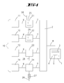
- the Fig. 1 shows an embodiment of the invention.
- the reference numeral 10 designates a source arrangement consisting of four sources 11, 12, 13, 14 in the exemplary embodiment. According to the invention, however, only a single source 11 needs to be present. These single or in the embodiment four sources 11, 12, 13, 14 are each with gas lines 6 with a respective source 11, 12, 13, 14 individually associated modification chamber 21, 22, 23, 24 connected. Each of the modification chambers 21, 22, 23, 24 is connected to a mixing chamber 2. This is done via the gas line designated by the reference numeral 7. Alternatively, one or more sources 11, 12, 13, 14 may be connected directly to the mixing chamber 2 without the interposition of a modification chamber.
- a deposition chamber 1 Downstream of the mixing chamber there is a deposition chamber 1 connected to the gas line 8 with the mixing chamber 2. This has a gas inlet system 3, which is fed by the gas line 8. Below the gas inlet member 3 is a deposition chamber whose bottom is formed by a water-cooled susceptor 4. On the susceptor 4 is a substrate 5, for example in the form of a glass sheet, which is to be coated with an electronic, light-emitting or photovoltaic layer of organic molecules.
- the total pressure in the process chamber is greater than 0.1 mbar and preferably greater than 1 mbar. It can also be greater than 10 mbar, so that the presence of the carrier gas can develop a kinetic effect.
- the organic molecules form solid, liquid or gaseous starting materials which are stored in the sources 11, 12, 13, 14. They are either converted by vaporization into the gas phase or converted by means of injection nozzles into aerosols, which can be transported via a carrier gas stream.
- One of the sources 11, 12, 13, 14 contains a material forming the layer, previously known as the matrix-forming starting material.
- one of the sources 11, 12, 13, 14 contains a starting material which is a precursor of a dopant.
- the modification chambers 21, 22, 23, 24 contain means with which the starting material flowing through this modification chamber 21, 22, 23, 24 can be modified.
- the modification can be a mere physical stimulation. However, it can also be a chemical reaction, for example an analysis or a synthesis. If the chemical reaction is a synthesis, a further reaction gas can be introduced into the modification chamber 21, 24 by means of a reaction gas feed line 26, whereby a plasma cell 27 can also be provided here, with which the reaction gas flowing through the reaction gas feed line 26 , is excited before entering the modification chamber.
- the modification within the modification chamber 21, 22 can take place via a plasma.
- a plasma generator 25 is provided in the modification chamber 21, 22, which generates a DC plasma or an AC plasma. With this plasma, physical excitations or chemical transformations / destruction of the molecules can be made. It is also possible to generate an RF field within a modification chamber 23 to excite or chemically transform the starting materials.
- a heater is provided as a power supply for the modification.
- reaction gas CO, H 2 , TMGa, CH 4 or NH 3 can be passed through the reaction gas line 26.
- H 2 and CH 4 are decomposed in the modification chamber 21 via the plasma generator 25.
- ions or radicals are formed, for example elemental hydrogen, elemental nitrogen or the like. These radicals can be incorporated n-doping in the matrix. These are reducing gases.
- oxidizing gases such as O 3 , N 2 O, O 2 , NO x , SF 6 , CF 4 or halogens such as F 2 , Cl 2 , Br 2 or I 2 may also be used.
- the reaction gases can be decomposed with a plasma into radicals or into ions. If the decomposition product is an ion, then the modification chambers 21, 22, 24 can also have electrostatic filters in order to influence the kinetic energy of these ions.
- Suitable starting materials for a p-doping or an n-doping are also all other chemical compounds known as dopants or precursors of dopants.
- matrix-forming starting materials such as alq 3 or ⁇ -NPD are also suitable.
- the latter are converted with the modification such that they acquire different electronic or optical properties.
Landscapes
- Chemical & Material Sciences (AREA)
- Engineering & Computer Science (AREA)
- Metallurgy (AREA)
- Organic Chemistry (AREA)
- Mechanical Engineering (AREA)
- Chemical Kinetics & Catalysis (AREA)
- Materials Engineering (AREA)
- Physics & Mathematics (AREA)
- Manufacturing & Machinery (AREA)
- Nanotechnology (AREA)
- Optics & Photonics (AREA)
- Mathematical Physics (AREA)
- Theoretical Computer Science (AREA)
- Crystallography & Structural Chemistry (AREA)
- Electroluminescent Light Sources (AREA)
- Chemical Vapour Deposition (AREA)
- Physical Vapour Deposition (AREA)
Applications Claiming Priority (1)
| Application Number | Priority Date | Filing Date | Title |
|---|---|---|---|
| DE102007030499A DE102007030499A1 (de) | 2007-06-30 | 2007-06-30 | Vorrichtung und Verfahren zum Abscheiden von insbesondere dotierten Schichten mittels OVPD oder dergleichen |
Publications (3)
| Publication Number | Publication Date |
|---|---|
| EP2009714A2 true EP2009714A2 (fr) | 2008-12-31 |
| EP2009714A3 EP2009714A3 (fr) | 2012-02-29 |
| EP2009714B1 EP2009714B1 (fr) | 2018-12-05 |
Family
ID=39862959
Family Applications (1)
| Application Number | Title | Priority Date | Filing Date |
|---|---|---|---|
| EP08159270.1A Not-in-force EP2009714B1 (fr) | 2007-06-30 | 2008-06-27 | Dispositif et procédé de déposition de couches dotées à l'aide d'OVPD ou similaire |
Country Status (3)
| Country | Link |
|---|---|
| US (1) | US8304013B2 (fr) |
| EP (1) | EP2009714B1 (fr) |
| DE (1) | DE102007030499A1 (fr) |
Cited By (1)
| Publication number | Priority date | Publication date | Assignee | Title |
|---|---|---|---|---|
| WO2016037964A1 (fr) * | 2014-09-08 | 2016-03-17 | Cynora Gmbh | Couche optiquement active améliorée et procédé pour la réaliser |
Families Citing this family (4)
| Publication number | Priority date | Publication date | Assignee | Title |
|---|---|---|---|---|
| DE102014100135A1 (de) | 2014-01-08 | 2015-07-09 | Aixtron Se | Gasmischvorrichtung an einem Reaktor mit Wegeventil |
| JP2016222984A (ja) * | 2015-06-01 | 2016-12-28 | 株式会社フィルテック | ヒートビーム成膜装置 |
| KR102369676B1 (ko) | 2017-04-10 | 2022-03-04 | 삼성디스플레이 주식회사 | 표시 장치의 제조장치 및 표시 장치의 제조방법 |
| KR20190090414A (ko) * | 2018-01-24 | 2019-08-02 | 삼성디스플레이 주식회사 | 증착 장치 |
Citations (5)
| Publication number | Priority date | Publication date | Assignee | Title |
|---|---|---|---|---|
| DD279032A1 (de) | 1988-12-30 | 1990-05-23 | Elektronische Bauelemente Veb | Verfahren zur herstellung duenner organischer halbleiterschichten |
| US5554220A (en) | 1995-05-19 | 1996-09-10 | The Trustees Of Princeton University | Method and apparatus using organic vapor phase deposition for the growth of organic thin films with large optical non-linearities |
| US6207238B1 (en) | 1998-12-16 | 2001-03-27 | Battelle Memorial Institute | Plasma enhanced chemical deposition for high and/or low index of refraction polymers |
| DE10338406A1 (de) | 2003-08-18 | 2005-03-24 | Novaled Gmbh | Dotierte organische Halbleitermaterialien sowie Verfahren zu deren Herstellung |
| US7201942B2 (en) | 2000-02-16 | 2007-04-10 | Aixtron Ag | Coating method |
Family Cites Families (10)
| Publication number | Priority date | Publication date | Assignee | Title |
|---|---|---|---|---|
| US5156815A (en) * | 1988-09-08 | 1992-10-20 | Board Of Regents, The University Of Texas System | Sublimating and cracking apparatus |
| DE19822333A1 (de) * | 1998-05-19 | 1999-12-02 | Lutz Kipp | Verfahren zur p-Dotierung von Fulleriten insbesondere zur Herstellung wenigstens eines Teils eines elektronischen Bauelements und ein p-dotiertes Fullerit |
| US6228436B1 (en) * | 1998-12-16 | 2001-05-08 | Battelle Memorial Institute | Method of making light emitting polymer composite material |
| WO2001099196A1 (fr) * | 2000-06-19 | 2001-12-27 | Yokohama Tlo Company, Ltd. | Element electronique pouvant fonctionner a temperature ambiante faisant intervenir un effet super-dielectrique |
| DE10207859A1 (de) * | 2002-02-20 | 2003-09-04 | Univ Dresden Tech | Dotiertes organisches Halbleitermaterial sowie Verfahren zu dessen Herstellung |
| DE10212923A1 (de) * | 2002-03-22 | 2004-01-08 | Aixtron Ag | Verfahren zum Beschichten eines Substrates und Vorrichtung zur Durchführung des Verfahrens |
| US20050109281A1 (en) * | 2002-03-22 | 2005-05-26 | Holger Jurgensen | Process for coating a substrate, and apparatus for carrying out the process |
| AU2003296882A1 (en) * | 2002-07-19 | 2004-05-04 | Ppg Industries Ohio, Inc. | Article having nano-scaled structures and a process for making such article |
| EP1607446B1 (fr) * | 2003-03-26 | 2016-09-07 | Semiconductor Energy Laboratory Co., Ltd. | Materiau hybride organique/inorganique, composition permettant de synthetiser ce matériau et processus de production de ce matériau hybride |
| US7238389B2 (en) * | 2004-03-22 | 2007-07-03 | Eastman Kodak Company | Vaporizing fluidized organic materials |
-
2007
- 2007-06-30 DE DE102007030499A patent/DE102007030499A1/de not_active Withdrawn
-
2008
- 2008-06-27 US US12/163,546 patent/US8304013B2/en not_active Expired - Fee Related
- 2008-06-27 EP EP08159270.1A patent/EP2009714B1/fr not_active Not-in-force
Patent Citations (5)
| Publication number | Priority date | Publication date | Assignee | Title |
|---|---|---|---|---|
| DD279032A1 (de) | 1988-12-30 | 1990-05-23 | Elektronische Bauelemente Veb | Verfahren zur herstellung duenner organischer halbleiterschichten |
| US5554220A (en) | 1995-05-19 | 1996-09-10 | The Trustees Of Princeton University | Method and apparatus using organic vapor phase deposition for the growth of organic thin films with large optical non-linearities |
| US6207238B1 (en) | 1998-12-16 | 2001-03-27 | Battelle Memorial Institute | Plasma enhanced chemical deposition for high and/or low index of refraction polymers |
| US7201942B2 (en) | 2000-02-16 | 2007-04-10 | Aixtron Ag | Coating method |
| DE10338406A1 (de) | 2003-08-18 | 2005-03-24 | Novaled Gmbh | Dotierte organische Halbleitermaterialien sowie Verfahren zu deren Herstellung |
Non-Patent Citations (4)
| Title |
|---|
| FENGHONG LI ET AL.: "Novel dopants for n-type doping of electron transport materials: cationic dyes and their bases", DISSERTATION, DIPL.-CHEM., January 2005 (2005-01-01) |
| P. E. BURROWS: "Organic Vapor Phase Depo sition: a New Method for the Growth of Organic Thin Films with Large Optical Non-linearities", CRYSTAL GROWTH, vol. 156, 1995, pages 91 |
| S. R. FORREST ET AL.: "Intense Second Harmonic Generation and Long-Range Structural Ordering in Thin Films of an Organic Salt Grown by Organic Vapor Phase Deposition", APPL. PHYS. LETT., vol. 68, 1996, pages 1326, XP000582290, DOI: doi:10.1063/1.115923 |
| SHIN-ICHIRO TAMURA: "A Blue Organic Light Emitting Diode", JPN. J. APPL. PHYS., vol. 38, no. 9A, 1999, pages 5274 - 5277 |
Cited By (1)
| Publication number | Priority date | Publication date | Assignee | Title |
|---|---|---|---|---|
| WO2016037964A1 (fr) * | 2014-09-08 | 2016-03-17 | Cynora Gmbh | Couche optiquement active améliorée et procédé pour la réaliser |
Also Published As
| Publication number | Publication date |
|---|---|
| DE102007030499A1 (de) | 2009-01-08 |
| EP2009714A3 (fr) | 2012-02-29 |
| EP2009714B1 (fr) | 2018-12-05 |
| US8304013B2 (en) | 2012-11-06 |
| US20090004830A1 (en) | 2009-01-01 |
Similar Documents
| Publication | Publication Date | Title |
|---|---|---|
| DE102008011185A1 (de) | Verfahren zur Herstellung einer dotierten organischen halbleitenden Schicht | |
| DE102007014048B4 (de) | Mischung aus Matrixmaterial und Dotierungsmaterial, sowie Verfahren zum Herstellen einer Schicht aus dotiertem organischen Material | |
| DE102013109451B9 (de) | Verfahren zur Herstellung eines optoelektronischen Bauelements | |
| DE102008056391B4 (de) | Organisches elektronisches Bauelement und Verfahren zu dessen Herstellung | |
| DE10333232A1 (de) | Organisches Elektrolumineszenzelement | |
| WO2008058525A2 (fr) | Utilisation d'une liaison de coordination pour doper des semiconducteurs organiques | |
| DE102011003192B4 (de) | Halbleiterbauelement und Verfahren zu seiner Herstellung | |
| EP2009714B1 (fr) | Dispositif et procédé de déposition de couches dotées à l'aide d'OVPD ou similaire | |
| WO2006092135A1 (fr) | Composant photoactif a couches organiques | |
| DE112012001217T5 (de) | Struktur und Verfahren zur Herstellung von Graphen-Nanostreifen | |
| DE102013021223A1 (de) | Herstellung flexibler organischer elektronischer Vorrichtungen | |
| WO2014076276A1 (fr) | Procédé de fabrication d'une couche sur une zone de surface d'un composant électronique | |
| WO2016000944A1 (fr) | Procédé et dispositif de génération de la vapeur à partir de plusieurs matières de départ liquides ou solides pour dispositif cvd ou pvd | |
| DE102006054523B4 (de) | Dithiolenübergangsmetallkomplexe und Selen-analoge Verbindungen, deren Verwendung als Dotand, organisches halbleitendes Material enthaltend die Komplexe, sowie elektronische oder optoelektronisches Bauelement enthaltend einen Komplex | |
| EP1860709A1 (fr) | Utilisation des complexes plans quadrangulaires à base des métaux de transition | |
| DE202014106226U1 (de) | Organisches elektronisches Bauteil | |
| WO2006037300A2 (fr) | Procede et dispositif pour produire une couche constituee d'un materiau semi-conducteur dope | |
| WO2016116202A1 (fr) | Bases aminophosphazène en tant qu'agents de dopage de type n en électronique organique | |
| DE102008028542A1 (de) | Verfahren und Vorrichtung zum Abscheiden einer Schicht auf einem Substrat mittels einer plasmagestützten chemischen Reaktion | |
| EP0958241B1 (fr) | PROCEDE ET DISPOSITIF DE PRODUCTION DE FULLERENES ENDOEDRES STABLES DE STRUCTURE Z-at-Cx AVEC x SUPERIEUR OU EGAL A 60 | |
| WO2021078584A1 (fr) | Procédé de dépôt de structures de couches organiques, en particulier de diodes électroluminescentes organiques | |
| EP1783846B1 (fr) | Dépôt d'une couche organique dopée sur un substrat. | |
| DE102012102565A1 (de) | Verfahren zur Herstellung eines elektrischen Bauteils, Kodepositionsanlage und elektrisches Bauteil | |
| WO2019068607A1 (fr) | Procédé de fabrication d'un agencement de pixels lumineux | |
| WO2023131379A1 (fr) | Procédé de fabrication d'une couche photoactive dans un système de couches d'un composant électronique organique |
Legal Events
| Date | Code | Title | Description |
|---|---|---|---|
| PUAI | Public reference made under article 153(3) epc to a published international application that has entered the european phase |
Free format text: ORIGINAL CODE: 0009012 |
|
| AK | Designated contracting states |
Kind code of ref document: A2 Designated state(s): AT BE BG CH CY CZ DE DK EE ES FI FR GB GR HR HU IE IS IT LI LT LU LV MC MT NL NO PL PT RO SE SI SK TR |
|
| AX | Request for extension of the european patent |
Extension state: AL BA MK RS |
|
| RAP1 | Party data changed (applicant data changed or rights of an application transferred) |
Owner name: AIXTRON AG |
|
| RAP1 | Party data changed (applicant data changed or rights of an application transferred) |
Owner name: AIXTRON SE |
|
| RIC1 | Information provided on ipc code assigned before grant |
Ipc: H01L 51/00 20060101ALI20111013BHEP Ipc: B05D 7/24 20060101AFI20111013BHEP Ipc: C23C 14/22 20060101ALI20111013BHEP Ipc: C23C 14/54 20060101ALI20111013BHEP Ipc: H01L 51/52 20060101ALI20111013BHEP Ipc: H01L 51/56 20060101ALI20111013BHEP Ipc: C23C 14/12 20060101ALI20111013BHEP |
|
| PUAL | Search report despatched |
Free format text: ORIGINAL CODE: 0009013 |
|
| AK | Designated contracting states |
Kind code of ref document: A3 Designated state(s): AT BE BG CH CY CZ DE DK EE ES FI FR GB GR HR HU IE IS IT LI LT LU LV MC MT NL NO PL PT RO SE SI SK TR |
|
| AX | Request for extension of the european patent |
Extension state: AL BA MK RS |
|
| RIC1 | Information provided on ipc code assigned before grant |
Ipc: C23C 14/22 20060101ALI20120126BHEP Ipc: C23C 14/54 20060101ALI20120126BHEP Ipc: H01L 51/52 20060101ALI20120126BHEP Ipc: H01L 51/56 20060101ALI20120126BHEP Ipc: C23C 14/12 20060101ALI20120126BHEP Ipc: H01L 51/00 20060101ALI20120126BHEP Ipc: C23C 14/24 20060101ALI20120126BHEP Ipc: B05D 1/00 20060101AFI20120126BHEP Ipc: C23C 14/32 20060101ALI20120126BHEP |
|
| 17P | Request for examination filed |
Effective date: 20120719 |
|
| AKX | Designation fees paid |
Designated state(s): DE FR GB NL |
|
| RAP1 | Party data changed (applicant data changed or rights of an application transferred) |
Owner name: AIXTRON SE |
|
| STAA | Information on the status of an ep patent application or granted ep patent |
Free format text: STATUS: EXAMINATION IS IN PROGRESS |
|
| 17Q | First examination report despatched |
Effective date: 20180119 |
|
| GRAP | Despatch of communication of intention to grant a patent |
Free format text: ORIGINAL CODE: EPIDOSNIGR1 |
|
| STAA | Information on the status of an ep patent application or granted ep patent |
Free format text: STATUS: GRANT OF PATENT IS INTENDED |
|
| INTG | Intention to grant announced |
Effective date: 20180713 |
|
| GRAS | Grant fee paid |
Free format text: ORIGINAL CODE: EPIDOSNIGR3 |
|
| GRAA | (expected) grant |
Free format text: ORIGINAL CODE: 0009210 |
|
| GRAA | (expected) grant |
Free format text: ORIGINAL CODE: 0009210 |
|
| STAA | Information on the status of an ep patent application or granted ep patent |
Free format text: STATUS: THE PATENT HAS BEEN GRANTED |
|
| AK | Designated contracting states |
Kind code of ref document: B1 Designated state(s): DE FR GB NL |
|
| REG | Reference to a national code |
Ref country code: GB Ref legal event code: FG4D Free format text: NOT ENGLISH |
|
| REG | Reference to a national code |
Ref country code: DE Ref legal event code: R096 Ref document number: 502008016500 Country of ref document: DE |
|
| REG | Reference to a national code |
Ref country code: NL Ref legal event code: MP Effective date: 20181205 |
|
| PG25 | Lapsed in a contracting state [announced via postgrant information from national office to epo] |
Ref country code: NL Free format text: LAPSE BECAUSE OF FAILURE TO SUBMIT A TRANSLATION OF THE DESCRIPTION OR TO PAY THE FEE WITHIN THE PRESCRIBED TIME-LIMIT Effective date: 20181205 |
|
| REG | Reference to a national code |
Ref country code: DE Ref legal event code: R097 Ref document number: 502008016500 Country of ref document: DE |
|
| PLBE | No opposition filed within time limit |
Free format text: ORIGINAL CODE: 0009261 |
|
| STAA | Information on the status of an ep patent application or granted ep patent |
Free format text: STATUS: NO OPPOSITION FILED WITHIN TIME LIMIT |
|
| 26N | No opposition filed |
Effective date: 20190906 |
|
| GBPC | Gb: european patent ceased through non-payment of renewal fee |
Effective date: 20190627 |
|
| PG25 | Lapsed in a contracting state [announced via postgrant information from national office to epo] |
Ref country code: GB Free format text: LAPSE BECAUSE OF NON-PAYMENT OF DUE FEES Effective date: 20190627 |
|
| PG25 | Lapsed in a contracting state [announced via postgrant information from national office to epo] |
Ref country code: FR Free format text: LAPSE BECAUSE OF NON-PAYMENT OF DUE FEES Effective date: 20190630 |
|
| PGFP | Annual fee paid to national office [announced via postgrant information from national office to epo] |
Ref country code: DE Payment date: 20200716 Year of fee payment: 13 |
|
| REG | Reference to a national code |
Ref country code: DE Ref legal event code: R119 Ref document number: 502008016500 Country of ref document: DE |
|
| PG25 | Lapsed in a contracting state [announced via postgrant information from national office to epo] |
Ref country code: DE Free format text: LAPSE BECAUSE OF NON-PAYMENT OF DUE FEES Effective date: 20220101 |