EP2010500B1 - Dispositif de contact de semi-conducteurs de puissance sur une surface réfrigérante - Google Patents
Dispositif de contact de semi-conducteurs de puissance sur une surface réfrigérante Download PDFInfo
- Publication number
- EP2010500B1 EP2010500B1 EP07727781A EP07727781A EP2010500B1 EP 2010500 B1 EP2010500 B1 EP 2010500B1 EP 07727781 A EP07727781 A EP 07727781A EP 07727781 A EP07727781 A EP 07727781A EP 2010500 B1 EP2010500 B1 EP 2010500B1
- Authority
- EP
- European Patent Office
- Prior art keywords
- spring element
- cooling surface
- housing
- arrangement according
- spring
- Prior art date
- Legal status (The legal status is an assumption and is not a legal conclusion. Google has not performed a legal analysis and makes no representation as to the accuracy of the status listed.)
- Active
Links
Images
Classifications
-
- H—ELECTRICITY
- H10—SEMICONDUCTOR DEVICES; ELECTRIC SOLID-STATE DEVICES NOT OTHERWISE PROVIDED FOR
- H10W—GENERIC PACKAGES, INTERCONNECTIONS, CONNECTORS OR OTHER CONSTRUCTIONAL DETAILS OF DEVICES COVERED BY CLASS H10
- H10W40/00—Arrangements for thermal protection or thermal control
- H10W40/60—Securing means for detachable heating or cooling arrangements, e.g. clamps
- H10W40/641—Snap-on arrangements, e.g. clips
-
- A—HUMAN NECESSITIES
- A61—MEDICAL OR VETERINARY SCIENCE; HYGIENE
- A61P—SPECIFIC THERAPEUTIC ACTIVITY OF CHEMICAL COMPOUNDS OR MEDICINAL PREPARATIONS
- A61P35/00—Antineoplastic agents
-
- H—ELECTRICITY
- H05—ELECTRIC TECHNIQUES NOT OTHERWISE PROVIDED FOR
- H05K—PRINTED CIRCUITS; CASINGS OR CONSTRUCTIONAL DETAILS OF ELECTRIC APPARATUS; MANUFACTURE OF ASSEMBLAGES OF ELECTRICAL COMPONENTS
- H05K7/00—Constructional details common to different types of electric apparatus
- H05K7/20—Modifications to facilitate cooling, ventilating, or heating
- H05K7/2089—Modifications to facilitate cooling, ventilating, or heating for power electronics, e.g. for inverters for controlling motor
- H05K7/209—Heat transfer by conduction from internal heat source to heat radiating structure
Definitions
- the present invention relates to an arrangement for contacting at least one electronic component mounted in a housing with connecting wires, in particular a power semiconductor, on a cooling surface and a spring element fastened in the housing with at least one spring arm which presses the component against the cooling surface in a contact position of the spring element ,
- the prior art further includes holding devices, which essentially comprise a U- or L-shaped spring clip which is (clipped ”) over ade Economicswandung and simultaneously over the component and in this way the pressing force between the contact surfaces of the heat sink and ensures the component.
- the present invention is based on the object to provide an arrangement of the type described above, which exerts no shear forces in the direction or opposite direction of the connecting wires for the electrical components with simple installation.
- the above-mentioned object is achieved in that the housing wall in the adjoining the side wall acting as a cooling surface side walls perpendicular to the bottom to running embedded pairs of grooves, each consisting of an insertion groove and a locking groove, wherein the Einhegenuten are deart .
- the locking grooves allow a convenient automatic engagement of the spring element in a predefined position. A complex alignment of the spring element is eliminated.
- the spring element is displaceable from the first mounting position by a force perpendicular to the cooling surface in the pressing position, so that in this second assembly step no thrust force acts in the longitudinal direction of the connecting wires, instead, the spring element from the first mounting position by acting purely perpendicular to the cooling surface forces fixed in the pressure position.
- the spring element consists of mutually parallel spring arms, which are perpendicularly attached to a support member which connects the two lateral projections of the spring element with each other
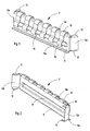
- the Fig. 1 and 2 show an inventive spring element 2 as provided for installation in an electronics housing 4 of an electric motor.
- the spring element 2 consists of a support member 8, at the upper edge present z. B. six spring arms 10 are formed and the side has two angled lugs 12 a, 12 b.
- the lugs 12a, 12b are formed at their upper and lower edges with folded at right angles inwardly tabs 13 to prevent buckling of the lugs 12a, 12b.
- the support member has approximately right angle folded narrow portions 14a, 14b, the bottom portion 14a facing the side where the spring arms 10 are and the top portion 14b faces in the opposite direction.
- the upper section 14b continues at equidistant intervals ( Fig.
- the spring arms 10 At its lower end, the spring arms 10 have a convex outwardly curved contact portion 16 which in Anyakposition of the spring element 2 against the Components 24 presses.
- a convex outwardly curved contact portion 16 Below the center of the support member 8, opposite the contact portions 16, parallel to the top and bottom edges of the support member 8 is a curved towards the front, semicircular stiffening bead 18, which prevents bending of the spring element 2.
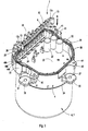
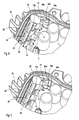
- the Fig. 3 to 7 show a possible use variant of the spring element 2 according to the invention in an electronics housing 4 of an electric motor 6.
- the electronics housing 4 On a rotor housing 7 of the electric motor 6, the electronics housing 4 is placed, which receives a printed circuit board 20 with electronic components 22 and other electrical connecting elements ( Fig. 3 ).
- the electronics housing 4 consists essentially of a peripheral wall, which is formed by a flat side wall 26, which acts as a cooling surface, adjoining side walls 32, 33 and one of the planar side wall 26 opposite wall 34.
- brackets 36 are formed with holes 37 for attachment of the housing.
- the electronics housing 4 can be closed with a housing cover, not shown, which engages in a circumferential groove 38 on the end face of the side walls 26, 32, 33 and 34.
- the housing cover is attached to holding projections 40, the holes 41, attached.
- On the bottom of the electronics housing 4 sits a electronic components 22, 24 supporting circuit board 20.
- Power semiconductors 24 are soldered to the circuit board 20 that they can be arranged in the interior of the electronics housing 4 on a flat side wall 26 of the electronics housing 4. Between the power semiconductor 24 and the planar side wall 26, a heat conductive electrical insulating layer 28 is inserted to allow and improve heat transfer to the side wall 26 provided with cooling fins 30.
- the upper pair of tabs 13 has an additional task: If the * spring element 2 is inserted into the electronics housing 4, but not yet locked, a housing cover can not be mounted, as then molded on the housing cover pin on the upper tabs 13th rest and would prevent closure of the lid. If the proper locking of the spring element 2 is performed, the pin of the lid can engage in the vacant space and the lid can be put on. This has a check whether a proper assembly of the spring element 2 has been performed.
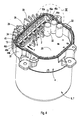
- the insertion position is in Fig. 4 shown. A detailed view of the position of the spring element in this insertion position shows Fig. 6 , It can be seen that the projection 12a is fixed by placing its end portion in the insertion groove 44a. In the insertion process, the spring arms 10 are not yet in contact with the power semiconductors 24, thus exerting no shear forces on the component 24 and its solder joint. It an air gap 45 remains between the spring arms 10 and the power semiconductors 24.
- the latching groove pair 46a, 46b adjoins directly to the insertion grooves 44a, 44b and is recessed in the same way but at a smaller distance from the flat side wall 26.
- the transition region 48a, 48b between the insertion groove 44a (44b) and the latching groove 46a (46b) is formed in such a way that its resistance can be overcome by a force F acting on the spring element 2 perpendicular to the cooling surface ( Fig. 4 ).
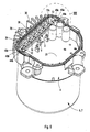
- the elastic lateral projections 12a, 12b are briefly compressed during the advancing movement in the direction of the power semiconductor 24 by the transition regions 48a, 48b before they rest in the latching grooves 46a, 46b in the pressure position ( Fig. 5 ).
- FIG. 7 A detailed view of the position of the spring element 2 on the side wall 32 in the pressure position shows Fig. 7 , The end portion of the projection 12a fixed with its vertically extending edge, which is now embedded in the locking groove 46a, the spring element 2.
- this pressure position now press the spring arms 10 on the power semiconductor 24, which thereby against the heat-conducting insulating layer 28 and thus against as Cooling surface 27 formed side wall 26 are pressed. This ensures safe heat dissipation without the use of other fasteners, such as screws or clamps.
- the component 24 and the solder joint are not loaded by shear forces.
Landscapes
- Microelectronics & Electronic Packaging (AREA)
- Engineering & Computer Science (AREA)
- Health & Medical Sciences (AREA)
- Thermal Sciences (AREA)
- Physics & Mathematics (AREA)
- Life Sciences & Earth Sciences (AREA)
- Veterinary Medicine (AREA)
- Pharmacology & Pharmacy (AREA)
- Nuclear Medicine, Radiotherapy & Molecular Imaging (AREA)
- Animal Behavior & Ethology (AREA)
- General Health & Medical Sciences (AREA)
- Public Health (AREA)
- Organic Chemistry (AREA)
- Medicinal Chemistry (AREA)
- General Chemical & Material Sciences (AREA)
- Chemical Kinetics & Catalysis (AREA)
- Chemical & Material Sciences (AREA)
- Cooling Or The Like Of Electrical Apparatus (AREA)
- Cooling Or The Like Of Semiconductors Or Solid State Devices (AREA)
Claims (8)
- Dispositif pour la mise en contact d'au moins un composant électronique (24), en particulier un semi-conducteur de puissance (24), sur une surface de refroidissement (26), formé par un boîtier (4), sur la surface de refroidissement (26) duquel le composant électronique (24) est monté avec des fils de raccordement, et par un élément de ressort (2), apte à être fixé dans le boîtier (4) et comportant au moins un bras de ressort (10) qui, dans une position de pression de l'élément de ressort (2), pousse le composant (24) contre la surface de refroidissement (26), et l'élément de ressort (2) peut être introduit dans le boîtier (4) sans entrer en contact avec le composant (24), et le boîtier (4) est muni de moyens de fixation (46a, 46b) pour l'élément de ressort (2), de telle sorte qu'aucune force de poussée ne se produit dans le sens longitudinal des fils de raccordement au moment du montage de l'élément de ressort (2),
caractérisé en ce que la paroi du boîtier, dans les parois latérales (32, 33) adjacentes à la paroi latérale (26) faisant fonction de surface de refroidissement, comporte des paires de rainures noyées, qui s'étendent perpendiculairement vers le bas vers le fond et qui sont formées par une rainure d'insertion (44a, 44b) et une rainure de blocage (46a, 46b), les rainures d'insertion (44a, 44b) étant telles que l'élément de ressort (2) peut être inséré dans la direction axiale (R) des rainures d'insertion sans entrer en contact avec le semi-conducteur de puissance (24) parallèlement à la surface de refroidissement (26) dans une position d'insertion, au moyen de saillies (12a, 12b) élastiques, pliées latéralement sur un élément de support de l'élément de ressort, et les rainures de blocage (46a, 46b) sont reliées aux rainures d'insertion (44a, 44b) par des zones de transition (48a, 48b) formées de telle sorte que l'élément de ressort (2) situé dans la position d'insertion peut être déplacé dans la position de pression bloquée, au moyen des saillies (12a, 12b) sous l'effet d'une force (F) agissant perpendiculairement à la surface de refroidissement (26), et les rainures de blocage (46a, 46b) sont réalisées de telle sorte qu'elles maintiennent l'élément de ressort (2) dans la position de pression. - Dispositif selon la revendication 1, caractérisé en ce que plusieurs bras de ressort (10) sont fixés parallèlement entre eux sur le bord de l'élément de support (8), détourné de la plaquette de circuits imprimés dans la position de montage de celle-ci.
- Dispositif selon l'une quelconque des revendications 1 à 2, caractérisé en ce que l'élément de support (8) comporte une nervure de raidissement (18) qui s'étend entre les deux saillies latérales (12a, 12b).
- Dispositif selon l'une quelconque des revendications 1 à 3, caractérisé en ce que l'élément de support (8) comporte sur ses côtés longitudinaux des segments (14a, 14b) repliés perpendiculairement.
- Dispositif selon l'une quelconque des revendications 1 à 4, caractérisé en ce que les saillies latérales (12a, 12b) de l'élément de ressort (2) comportent des pattes (13) formées perpendiculairement sur celles-ci.
- Dispositif selon l'une quelconque des revendications 1 à 5, caractérisé en ce que plusieurs composants (24), agencés avec la même orientation en une rangée, sont pressés par un élément de ressort (2).
- Dispositif selon l'une quelconque des revendications 1 à 6, caractérisé en ce que la paroi latérale (26), réalisée sous forme de surface de refroidissement (26), comporte une surface d'appui plane et parallèle, dirigée vers l'intérieur du boîtier, et comporte des ailettes de refroidissement (30) sur sa face extérieure.
- Dispositif selon l'une quelconque des revendications 1 à 6, caractérisé en ce qu'une couche isolante (28) électroconductrice est déposée entre la surface de refroidissement (26) et le composant (24).
Applications Claiming Priority (2)
| Application Number | Priority Date | Filing Date | Title |
|---|---|---|---|
| DE102006018716A DE102006018716A1 (de) | 2006-04-20 | 2006-04-20 | Anordnung zur Kontaktierung von Leistungshalbleitern an einer Kühlfläche |
| PCT/EP2007/053310 WO2007122084A1 (fr) | 2006-04-20 | 2007-04-04 | Dispositif de contact de semi-conducteurs de puissance sur une surface réfrigérante |
Publications (2)
| Publication Number | Publication Date |
|---|---|
| EP2010500A1 EP2010500A1 (fr) | 2009-01-07 |
| EP2010500B1 true EP2010500B1 (fr) | 2011-06-08 |
Family
ID=38141192
Family Applications (1)
| Application Number | Title | Priority Date | Filing Date |
|---|---|---|---|
| EP07727781A Active EP2010500B1 (fr) | 2006-04-20 | 2007-04-04 | Dispositif de contact de semi-conducteurs de puissance sur une surface réfrigérante |
Country Status (6)
| Country | Link |
|---|---|
| US (1) | US7845994B2 (fr) |
| EP (1) | EP2010500B1 (fr) |
| CN (1) | CN101421246B (fr) |
| AT (1) | ATE512461T1 (fr) |
| DE (1) | DE102006018716A1 (fr) |
| WO (1) | WO2007122084A1 (fr) |
Cited By (15)
| Publication number | Priority date | Publication date | Assignee | Title |
|---|---|---|---|---|
| US8839815B2 (en) | 2011-12-15 | 2014-09-23 | Honeywell International Inc. | Gas valve with electronic cycle counter |
| US8899264B2 (en) | 2011-12-15 | 2014-12-02 | Honeywell International Inc. | Gas valve with electronic proof of closure system |
| US8905063B2 (en) | 2011-12-15 | 2014-12-09 | Honeywell International Inc. | Gas valve with fuel rate monitor |
| US8947242B2 (en) | 2011-12-15 | 2015-02-03 | Honeywell International Inc. | Gas valve with valve leakage test |
| US9074770B2 (en) | 2011-12-15 | 2015-07-07 | Honeywell International Inc. | Gas valve with electronic valve proving system |
| US9234661B2 (en) | 2012-09-15 | 2016-01-12 | Honeywell International Inc. | Burner control system |
| US9557059B2 (en) | 2011-12-15 | 2017-01-31 | Honeywell International Inc | Gas valve with communication link |
| US9995486B2 (en) | 2011-12-15 | 2018-06-12 | Honeywell International Inc. | Gas valve with high/low gas pressure detection |
| US10024439B2 (en) | 2013-12-16 | 2018-07-17 | Honeywell International Inc. | Valve over-travel mechanism |
| US10203049B2 (en) | 2014-09-17 | 2019-02-12 | Honeywell International Inc. | Gas valve with electronic health monitoring |
| US10215291B2 (en) | 2013-10-29 | 2019-02-26 | Honeywell International Inc. | Regulating device |
| US10564062B2 (en) | 2016-10-19 | 2020-02-18 | Honeywell International Inc. | Human-machine interface for gas valve |
| US10697815B2 (en) | 2018-06-09 | 2020-06-30 | Honeywell International Inc. | System and methods for mitigating condensation in a sensor module |
| US10851993B2 (en) | 2011-12-15 | 2020-12-01 | Honeywell International Inc. | Gas valve with overpressure diagnostics |
| US11073281B2 (en) | 2017-12-29 | 2021-07-27 | Honeywell International Inc. | Closed-loop programming and control of a combustion appliance |
Families Citing this family (14)
| Publication number | Priority date | Publication date | Assignee | Title |
|---|---|---|---|---|
| DK2227078T3 (da) * | 2009-03-04 | 2012-02-20 | Ebm Papst Mulfingen Gmbh & Co | Spændekomponent til at trykke ydelseskomponenter fast til en køleflade |
| JP5609596B2 (ja) * | 2010-12-01 | 2014-10-22 | アイシン・エィ・ダブリュ株式会社 | 熱源素子と熱伝導性部材との固定構造、及び熱源素子と熱伝導性部材との固定方法 |
| US8668528B2 (en) | 2011-10-28 | 2014-03-11 | Apple Inc. | Split jack assemblies and methods for making the same |
| JP5892691B2 (ja) * | 2011-12-15 | 2016-03-23 | 太陽誘電株式会社 | 電子装置 |
| US9846440B2 (en) | 2011-12-15 | 2017-12-19 | Honeywell International Inc. | Valve controller configured to estimate fuel comsumption |
| US9835265B2 (en) | 2011-12-15 | 2017-12-05 | Honeywell International Inc. | Valve with actuator diagnostics |
| JP5408285B2 (ja) * | 2012-04-27 | 2014-02-05 | ダイキン工業株式会社 | 冷却器、電装品ユニット及び冷凍装置 |
| US10422531B2 (en) | 2012-09-15 | 2019-09-24 | Honeywell International Inc. | System and approach for controlling a combustion chamber |
| US9841122B2 (en) | 2014-09-09 | 2017-12-12 | Honeywell International Inc. | Gas valve with electronic valve proving system |
| US10503181B2 (en) | 2016-01-13 | 2019-12-10 | Honeywell International Inc. | Pressure regulator |
| CN109428497B (zh) * | 2017-08-23 | 2020-09-18 | 台达电子企业管理(上海)有限公司 | 电源模块的组装结构及其组装方法 |
| EP3634096A1 (fr) * | 2018-10-02 | 2020-04-08 | Mahle International GmbH | Onduleur de puissance |
| EP3634095B1 (fr) * | 2018-10-02 | 2022-03-16 | Mahle International GmbH | Onduleur de puissance |
| CN109801886A (zh) * | 2019-01-08 | 2019-05-24 | 常州索维尔电子科技有限公司 | 一种压紧弹片以及散热结构 |
Family Cites Families (14)
| Publication number | Priority date | Publication date | Assignee | Title |
|---|---|---|---|---|
| US4707726A (en) | 1985-04-29 | 1987-11-17 | United Technologies Automotive, Inc. | Heat sink mounting arrangement for a semiconductor |
| DE9213671U1 (de) | 1991-11-11 | 1992-12-03 | Tridonic-Bauelemente GmbH, Dornbirn | Gehäuse für eine elektronische Schaltungsanordnung |
| US5274193A (en) | 1992-04-24 | 1993-12-28 | Chrysler Corporation | Heat sink spring and wedge assembly |
| US5466970A (en) * | 1992-08-24 | 1995-11-14 | Thermalloy, Inc. | Hooked spring clip |
| DE19543260C2 (de) | 1995-11-20 | 2001-09-20 | Robert Seuffer Gmbh & Co | Elektrische Bauelementeanordnung mit mehreren in einem Gehäuse angeordneten elektrischen Bauelementen |
| US5731955A (en) * | 1996-02-05 | 1998-03-24 | Ford Motor Company | Spring clip for electronics assembly |
| US5909358A (en) * | 1997-11-26 | 1999-06-01 | Todd Engineering Sales, Inc. | Snap-lock heat sink clip |
| FR2780456A1 (fr) | 1998-06-30 | 1999-12-31 | Valeo Electronique | Dispositif de blocage mecanique d'un element electrique ou electronique sur un support |
| JP4060510B2 (ja) | 2000-03-02 | 2008-03-12 | カルソニックカンセイ株式会社 | パワー素子の放熱部材への取付構造 |
| DE20014739U1 (de) | 2000-08-28 | 2000-12-14 | Fischer-Elektronik GmbH & Co. KG, 58511 Lüdenscheid | Vorrichtung zur Halterung von elektronischen Bauteilen |
| DE10237871B4 (de) * | 2002-08-19 | 2011-05-12 | Infineon Technologies Ag | Baugruppensystem |
| DE10317182B4 (de) | 2003-04-15 | 2005-08-18 | Lear Corporation Gmbh & Co. Kg | Befestigungseinrichtung für mindestens ein elektronisches Bauelement an einem Kühlkörper |
| US7056144B2 (en) * | 2004-02-19 | 2006-06-06 | Hewlett-Packard Development Company, L.P. | Offset compensation system |
| US7190589B2 (en) * | 2004-10-19 | 2007-03-13 | Cinch Connectors, Inc. | Electronic control enclosure |
-
2006
- 2006-04-20 DE DE102006018716A patent/DE102006018716A1/de not_active Withdrawn
-
2007
- 2007-04-04 CN CN2007800137515A patent/CN101421246B/zh active Active
- 2007-04-04 AT AT07727781T patent/ATE512461T1/de active
- 2007-04-04 WO PCT/EP2007/053310 patent/WO2007122084A1/fr not_active Ceased
- 2007-04-04 EP EP07727781A patent/EP2010500B1/fr active Active
- 2007-04-04 US US12/297,837 patent/US7845994B2/en active Active
Cited By (16)
| Publication number | Priority date | Publication date | Assignee | Title |
|---|---|---|---|---|
| US10697632B2 (en) | 2011-12-15 | 2020-06-30 | Honeywell International Inc. | Gas valve with communication link |
| US9557059B2 (en) | 2011-12-15 | 2017-01-31 | Honeywell International Inc | Gas valve with communication link |
| US8905063B2 (en) | 2011-12-15 | 2014-12-09 | Honeywell International Inc. | Gas valve with fuel rate monitor |
| US8947242B2 (en) | 2011-12-15 | 2015-02-03 | Honeywell International Inc. | Gas valve with valve leakage test |
| US9074770B2 (en) | 2011-12-15 | 2015-07-07 | Honeywell International Inc. | Gas valve with electronic valve proving system |
| US8899264B2 (en) | 2011-12-15 | 2014-12-02 | Honeywell International Inc. | Gas valve with electronic proof of closure system |
| US10851993B2 (en) | 2011-12-15 | 2020-12-01 | Honeywell International Inc. | Gas valve with overpressure diagnostics |
| US8839815B2 (en) | 2011-12-15 | 2014-09-23 | Honeywell International Inc. | Gas valve with electronic cycle counter |
| US9995486B2 (en) | 2011-12-15 | 2018-06-12 | Honeywell International Inc. | Gas valve with high/low gas pressure detection |
| US9234661B2 (en) | 2012-09-15 | 2016-01-12 | Honeywell International Inc. | Burner control system |
| US10215291B2 (en) | 2013-10-29 | 2019-02-26 | Honeywell International Inc. | Regulating device |
| US10024439B2 (en) | 2013-12-16 | 2018-07-17 | Honeywell International Inc. | Valve over-travel mechanism |
| US10203049B2 (en) | 2014-09-17 | 2019-02-12 | Honeywell International Inc. | Gas valve with electronic health monitoring |
| US10564062B2 (en) | 2016-10-19 | 2020-02-18 | Honeywell International Inc. | Human-machine interface for gas valve |
| US11073281B2 (en) | 2017-12-29 | 2021-07-27 | Honeywell International Inc. | Closed-loop programming and control of a combustion appliance |
| US10697815B2 (en) | 2018-06-09 | 2020-06-30 | Honeywell International Inc. | System and methods for mitigating condensation in a sensor module |
Also Published As
| Publication number | Publication date |
|---|---|
| WO2007122084A1 (fr) | 2007-11-01 |
| ATE512461T1 (de) | 2011-06-15 |
| US7845994B2 (en) | 2010-12-07 |
| US20090239424A1 (en) | 2009-09-24 |
| DE102006018716A1 (de) | 2007-10-25 |
| EP2010500A1 (fr) | 2009-01-07 |
| CN101421246A (zh) | 2009-04-29 |
| CN101421246B (zh) | 2011-07-06 |
Similar Documents
| Publication | Publication Date | Title |
|---|---|---|
| EP2010500A1 (fr) | Dispositif de contact de semi-conducteurs de puissance sur une surface réfrigérante | |
| DE10392749B4 (de) | Kontrollmodulgehäuse für ein Fahrzeug | |
| DE102009046014B4 (de) | Elektrisches Verbindergehäuse und Verfahren zu dessen Zusammenbau | |
| EP0446320B1 (fr) | Boitier pour circuit electronique | |
| DE19722602C2 (de) | Wärmeableitendes Gehäuse zur Aufnahme von elektrischen oder elektronischen Bauteilen | |
| DE3627372C2 (fr) | ||
| WO2003107418A1 (fr) | Dissipateur thermique | |
| WO2008077858A1 (fr) | Support | |
| EP2450658B1 (fr) | Dispositif de fixation d'un condensateur | |
| WO2018219769A1 (fr) | Dispositif de fixation de composant | |
| DE102018106185B4 (de) | Kontaktelement mit einem Kontaktkörper und einem daran angeordneten Federelement | |
| DE19543260C2 (de) | Elektrische Bauelementeanordnung mit mehreren in einem Gehäuse angeordneten elektrischen Bauelementen | |
| EP3766130B1 (fr) | Élément de contact pourvu d'un corps de contact et d'un élément élastique agencé contre ce dernier | |
| EP2553736A2 (fr) | Élément de liaison, connecteur électrique et arrangement de liaison pour des modules de cellules solaires | |
| DE19708912C1 (de) | Schutzleiteranschlußklemme, insbesondere in einem Reihenklemmengehäuse | |
| WO1991011897A1 (fr) | Fixation pour des composants electroniques a refroidir | |
| DE10334629B3 (de) | Schaltungsmodul und Verfahren zu dessen Herstellung | |
| DE10206271A1 (de) | Wärmeableitvorrichtung | |
| DE20014739U1 (de) | Vorrichtung zur Halterung von elektronischen Bauteilen | |
| DE102015116639B4 (de) | Schnappverbindungsanordnung mit einem Schnapphakenelement und einem Schnapphakengegenelement | |
| EP1750302B1 (fr) | Arrangement des éléments électriques | |
| DE202013104941U1 (de) | Elektrische Steckverbinderanordnung und Schirmanbindungselement hierzu | |
| EP0123040A2 (fr) | Plaque à bornes pour des appareils électriques ou électroniques, par exemple pour un interrupteur de protection contre la surintensité | |
| DE102019134369B4 (de) | Leadframe für Drahtbauteile mit Kulissenstruktur | |
| EP1864557B1 (fr) | Procede de production d'un appareil electronique, et appareil electronique |
Legal Events
| Date | Code | Title | Description |
|---|---|---|---|
| PUAI | Public reference made under article 153(3) epc to a published international application that has entered the european phase |
Free format text: ORIGINAL CODE: 0009012 |
|
| 17P | Request for examination filed |
Effective date: 20081006 |
|
| AK | Designated contracting states |
Kind code of ref document: A1 Designated state(s): AT BE BG CH CY CZ DE DK EE ES FI FR GB GR HU IE IS IT LI LT LU LV MC MT NL PL PT RO SE SI SK TR |
|
| AX | Request for extension of the european patent |
Extension state: AL BA HR MK RS |
|
| 17Q | First examination report despatched |
Effective date: 20091120 |
|
| RTI1 | Title (correction) |
Free format text: ARRANGEMENT FOR CONTACTING POWER SEMICONDUCTORS TO A COOLING SURFACE |
|
| GRAP | Despatch of communication of intention to grant a patent |
Free format text: ORIGINAL CODE: EPIDOSNIGR1 |
|
| RIC1 | Information provided on ipc code assigned before grant |
Ipc: H05K 7/20 20060101ALI20101206BHEP Ipc: H01L 23/40 20060101AFI20101206BHEP |
|
| GRAS | Grant fee paid |
Free format text: ORIGINAL CODE: EPIDOSNIGR3 |
|
| GRAA | (expected) grant |
Free format text: ORIGINAL CODE: 0009210 |
|
| AK | Designated contracting states |
Kind code of ref document: B1 Designated state(s): AT BE BG CH CY CZ DE DK EE ES FI FR GB GR HU IE IS IT LI LT LU LV MC MT NL PL PT RO SE SI SK TR |
|
| REG | Reference to a national code |
Ref country code: GB Ref legal event code: FG4D Free format text: NOT ENGLISH |
|
| REG | Reference to a national code |
Ref country code: CH Ref legal event code: EP |
|
| REG | Reference to a national code |
Ref country code: IE Ref legal event code: FG4D Free format text: LANGUAGE OF EP DOCUMENT: GERMAN |
|
| REG | Reference to a national code |
Ref country code: DE Ref legal event code: R096 Ref document number: 502007007381 Country of ref document: DE Effective date: 20110721 |
|
| REG | Reference to a national code |
Ref country code: SE Ref legal event code: TRGR |
|
| REG | Reference to a national code |
Ref country code: NL Ref legal event code: VDEP Effective date: 20110608 |
|
| PG25 | Lapsed in a contracting state [announced via postgrant information from national office to epo] |
Ref country code: LT Free format text: LAPSE BECAUSE OF FAILURE TO SUBMIT A TRANSLATION OF THE DESCRIPTION OR TO PAY THE FEE WITHIN THE PRESCRIBED TIME-LIMIT Effective date: 20110608 |
|
| PG25 | Lapsed in a contracting state [announced via postgrant information from national office to epo] |
Ref country code: FI Free format text: LAPSE BECAUSE OF FAILURE TO SUBMIT A TRANSLATION OF THE DESCRIPTION OR TO PAY THE FEE WITHIN THE PRESCRIBED TIME-LIMIT Effective date: 20110608 Ref country code: SI Free format text: LAPSE BECAUSE OF FAILURE TO SUBMIT A TRANSLATION OF THE DESCRIPTION OR TO PAY THE FEE WITHIN THE PRESCRIBED TIME-LIMIT Effective date: 20110608 Ref country code: ES Free format text: LAPSE BECAUSE OF FAILURE TO SUBMIT A TRANSLATION OF THE DESCRIPTION OR TO PAY THE FEE WITHIN THE PRESCRIBED TIME-LIMIT Effective date: 20110919 Ref country code: LV Free format text: LAPSE BECAUSE OF FAILURE TO SUBMIT A TRANSLATION OF THE DESCRIPTION OR TO PAY THE FEE WITHIN THE PRESCRIBED TIME-LIMIT Effective date: 20110608 Ref country code: GR Free format text: LAPSE BECAUSE OF FAILURE TO SUBMIT A TRANSLATION OF THE DESCRIPTION OR TO PAY THE FEE WITHIN THE PRESCRIBED TIME-LIMIT Effective date: 20110909 Ref country code: CY Free format text: LAPSE BECAUSE OF FAILURE TO SUBMIT A TRANSLATION OF THE DESCRIPTION OR TO PAY THE FEE WITHIN THE PRESCRIBED TIME-LIMIT Effective date: 20110608 |
|
| PG25 | Lapsed in a contracting state [announced via postgrant information from national office to epo] |
Ref country code: NL Free format text: LAPSE BECAUSE OF FAILURE TO SUBMIT A TRANSLATION OF THE DESCRIPTION OR TO PAY THE FEE WITHIN THE PRESCRIBED TIME-LIMIT Effective date: 20110608 |
|
| REG | Reference to a national code |
Ref country code: IE Ref legal event code: FD4D |
|
| PG25 | Lapsed in a contracting state [announced via postgrant information from national office to epo] |
Ref country code: IE Free format text: LAPSE BECAUSE OF FAILURE TO SUBMIT A TRANSLATION OF THE DESCRIPTION OR TO PAY THE FEE WITHIN THE PRESCRIBED TIME-LIMIT Effective date: 20110608 Ref country code: PT Free format text: LAPSE BECAUSE OF FAILURE TO SUBMIT A TRANSLATION OF THE DESCRIPTION OR TO PAY THE FEE WITHIN THE PRESCRIBED TIME-LIMIT Effective date: 20111010 Ref country code: IS Free format text: LAPSE BECAUSE OF FAILURE TO SUBMIT A TRANSLATION OF THE DESCRIPTION OR TO PAY THE FEE WITHIN THE PRESCRIBED TIME-LIMIT Effective date: 20111008 Ref country code: EE Free format text: LAPSE BECAUSE OF FAILURE TO SUBMIT A TRANSLATION OF THE DESCRIPTION OR TO PAY THE FEE WITHIN THE PRESCRIBED TIME-LIMIT Effective date: 20110608 Ref country code: CZ Free format text: LAPSE BECAUSE OF FAILURE TO SUBMIT A TRANSLATION OF THE DESCRIPTION OR TO PAY THE FEE WITHIN THE PRESCRIBED TIME-LIMIT Effective date: 20110608 |
|
| PG25 | Lapsed in a contracting state [announced via postgrant information from national office to epo] |
Ref country code: PL Free format text: LAPSE BECAUSE OF FAILURE TO SUBMIT A TRANSLATION OF THE DESCRIPTION OR TO PAY THE FEE WITHIN THE PRESCRIBED TIME-LIMIT Effective date: 20110608 Ref country code: RO Free format text: LAPSE BECAUSE OF FAILURE TO SUBMIT A TRANSLATION OF THE DESCRIPTION OR TO PAY THE FEE WITHIN THE PRESCRIBED TIME-LIMIT Effective date: 20110608 Ref country code: SK Free format text: LAPSE BECAUSE OF FAILURE TO SUBMIT A TRANSLATION OF THE DESCRIPTION OR TO PAY THE FEE WITHIN THE PRESCRIBED TIME-LIMIT Effective date: 20110608 |
|
| PLBE | No opposition filed within time limit |
Free format text: ORIGINAL CODE: 0009261 |
|
| STAA | Information on the status of an ep patent application or granted ep patent |
Free format text: STATUS: NO OPPOSITION FILED WITHIN TIME LIMIT |
|
| 26N | No opposition filed |
Effective date: 20120309 |
|
| PG25 | Lapsed in a contracting state [announced via postgrant information from national office to epo] |
Ref country code: DK Free format text: LAPSE BECAUSE OF FAILURE TO SUBMIT A TRANSLATION OF THE DESCRIPTION OR TO PAY THE FEE WITHIN THE PRESCRIBED TIME-LIMIT Effective date: 20110608 |
|
| REG | Reference to a national code |
Ref country code: DE Ref legal event code: R097 Ref document number: 502007007381 Country of ref document: DE Effective date: 20120309 |
|
| BERE | Be: lapsed |
Owner name: EBM-PAPST MULFINGEN G.M.B.H. & CO. KG Effective date: 20120430 |
|
| PG25 | Lapsed in a contracting state [announced via postgrant information from national office to epo] |
Ref country code: MC Free format text: LAPSE BECAUSE OF NON-PAYMENT OF DUE FEES Effective date: 20120430 |
|
| REG | Reference to a national code |
Ref country code: CH Ref legal event code: PL |
|
| GBPC | Gb: european patent ceased through non-payment of renewal fee |
Effective date: 20120404 |
|
| PG25 | Lapsed in a contracting state [announced via postgrant information from national office to epo] |
Ref country code: LI Free format text: LAPSE BECAUSE OF NON-PAYMENT OF DUE FEES Effective date: 20120430 Ref country code: CH Free format text: LAPSE BECAUSE OF NON-PAYMENT OF DUE FEES Effective date: 20120430 Ref country code: BE Free format text: LAPSE BECAUSE OF NON-PAYMENT OF DUE FEES Effective date: 20120430 Ref country code: GB Free format text: LAPSE BECAUSE OF NON-PAYMENT OF DUE FEES Effective date: 20120404 |
|
| REG | Reference to a national code |
Ref country code: AT Ref legal event code: MM01 Ref document number: 512461 Country of ref document: AT Kind code of ref document: T Effective date: 20120404 |
|
| PG25 | Lapsed in a contracting state [announced via postgrant information from national office to epo] |
Ref country code: BG Free format text: LAPSE BECAUSE OF FAILURE TO SUBMIT A TRANSLATION OF THE DESCRIPTION OR TO PAY THE FEE WITHIN THE PRESCRIBED TIME-LIMIT Effective date: 20110908 |
|
| PG25 | Lapsed in a contracting state [announced via postgrant information from national office to epo] |
Ref country code: AT Free format text: LAPSE BECAUSE OF NON-PAYMENT OF DUE FEES Effective date: 20120404 Ref country code: MT Free format text: LAPSE BECAUSE OF FAILURE TO SUBMIT A TRANSLATION OF THE DESCRIPTION OR TO PAY THE FEE WITHIN THE PRESCRIBED TIME-LIMIT Effective date: 20110608 |
|
| PG25 | Lapsed in a contracting state [announced via postgrant information from national office to epo] |
Ref country code: TR Free format text: LAPSE BECAUSE OF FAILURE TO SUBMIT A TRANSLATION OF THE DESCRIPTION OR TO PAY THE FEE WITHIN THE PRESCRIBED TIME-LIMIT Effective date: 20110608 |
|
| PG25 | Lapsed in a contracting state [announced via postgrant information from national office to epo] |
Ref country code: LU Free format text: LAPSE BECAUSE OF NON-PAYMENT OF DUE FEES Effective date: 20120404 |
|
| PG25 | Lapsed in a contracting state [announced via postgrant information from national office to epo] |
Ref country code: HU Free format text: LAPSE BECAUSE OF FAILURE TO SUBMIT A TRANSLATION OF THE DESCRIPTION OR TO PAY THE FEE WITHIN THE PRESCRIBED TIME-LIMIT Effective date: 20070404 |
|
| REG | Reference to a national code |
Ref country code: FR Ref legal event code: PLFP Year of fee payment: 10 |
|
| REG | Reference to a national code |
Ref country code: FR Ref legal event code: PLFP Year of fee payment: 11 |
|
| REG | Reference to a national code |
Ref country code: FR Ref legal event code: PLFP Year of fee payment: 12 |
|
| REG | Reference to a national code |
Ref country code: DE Ref legal event code: R082 Ref document number: 502007007381 Country of ref document: DE Representative=s name: PATENTANWAELTE STAEGER & SPERLING PARTNERSCHAF, DE |
|
| PGFP | Annual fee paid to national office [announced via postgrant information from national office to epo] |
Ref country code: DE Payment date: 20250417 Year of fee payment: 19 |
|
| PGFP | Annual fee paid to national office [announced via postgrant information from national office to epo] |
Ref country code: IT Payment date: 20250430 Year of fee payment: 19 |
|
| PGFP | Annual fee paid to national office [announced via postgrant information from national office to epo] |
Ref country code: FR Payment date: 20250422 Year of fee payment: 19 |
|
| PGFP | Annual fee paid to national office [announced via postgrant information from national office to epo] |
Ref country code: SE Payment date: 20250423 Year of fee payment: 19 |