EP2013373B1 - Verfahren und system zur aufbereitung eines aufdampfungsziels - Google Patents
Verfahren und system zur aufbereitung eines aufdampfungsziels Download PDFInfo
- Publication number
- EP2013373B1 EP2013373B1 EP07761416A EP07761416A EP2013373B1 EP 2013373 B1 EP2013373 B1 EP 2013373B1 EP 07761416 A EP07761416 A EP 07761416A EP 07761416 A EP07761416 A EP 07761416A EP 2013373 B1 EP2013373 B1 EP 2013373B1
- Authority
- EP
- European Patent Office
- Prior art keywords
- arc
- vapor deposition
- power supply
- energy
- target
- Prior art date
- Legal status (The legal status is an assumption and is not a legal conclusion. Google has not performed a legal analysis and makes no representation as to the accuracy of the status listed.)
- Active
Links
Images


Classifications
-
- C—CHEMISTRY; METALLURGY
- C23—COATING METALLIC MATERIAL; COATING MATERIAL WITH METALLIC MATERIAL; CHEMICAL SURFACE TREATMENT; DIFFUSION TREATMENT OF METALLIC MATERIAL; COATING BY VACUUM EVAPORATION, BY SPUTTERING, BY ION IMPLANTATION OR BY CHEMICAL VAPOUR DEPOSITION, IN GENERAL; INHIBITING CORROSION OF METALLIC MATERIAL OR INCRUSTATION IN GENERAL
- C23C—COATING METALLIC MATERIAL; COATING MATERIAL WITH METALLIC MATERIAL; SURFACE TREATMENT OF METALLIC MATERIAL BY DIFFUSION INTO THE SURFACE, BY CHEMICAL CONVERSION OR SUBSTITUTION; COATING BY VACUUM EVAPORATION, BY SPUTTERING, BY ION IMPLANTATION OR BY CHEMICAL VAPOUR DEPOSITION, IN GENERAL
- C23C14/00—Coating by vacuum evaporation, by sputtering or by ion implantation of the coating forming material
- C23C14/22—Coating by vacuum evaporation, by sputtering or by ion implantation of the coating forming material characterised by the process of coating
- C23C14/34—Sputtering
-
- C—CHEMISTRY; METALLURGY
- C23—COATING METALLIC MATERIAL; COATING MATERIAL WITH METALLIC MATERIAL; CHEMICAL SURFACE TREATMENT; DIFFUSION TREATMENT OF METALLIC MATERIAL; COATING BY VACUUM EVAPORATION, BY SPUTTERING, BY ION IMPLANTATION OR BY CHEMICAL VAPOUR DEPOSITION, IN GENERAL; INHIBITING CORROSION OF METALLIC MATERIAL OR INCRUSTATION IN GENERAL
- C23C—COATING METALLIC MATERIAL; COATING MATERIAL WITH METALLIC MATERIAL; SURFACE TREATMENT OF METALLIC MATERIAL BY DIFFUSION INTO THE SURFACE, BY CHEMICAL CONVERSION OR SUBSTITUTION; COATING BY VACUUM EVAPORATION, BY SPUTTERING, BY ION IMPLANTATION OR BY CHEMICAL VAPOUR DEPOSITION, IN GENERAL
- C23C14/00—Coating by vacuum evaporation, by sputtering or by ion implantation of the coating forming material
- C23C14/22—Coating by vacuum evaporation, by sputtering or by ion implantation of the coating forming material characterised by the process of coating
- C23C14/54—Controlling or regulating the coating process
-
- H—ELECTRICITY
- H01—ELECTRIC ELEMENTS
- H01J—ELECTRIC DISCHARGE TUBES OR DISCHARGE LAMPS
- H01J37/00—Discharge tubes with provision for introducing objects or material to be exposed to the discharge, e.g. for the purpose of examination or processing thereof
- H01J37/32—Gas-filled discharge tubes
- H01J37/32917—Plasma diagnostics
- H01J37/32935—Monitoring and controlling tubes by information coming from the object and/or discharge
-
- H—ELECTRICITY
- H01—ELECTRIC ELEMENTS
- H01J—ELECTRIC DISCHARGE TUBES OR DISCHARGE LAMPS
- H01J37/00—Discharge tubes with provision for introducing objects or material to be exposed to the discharge, e.g. for the purpose of examination or processing thereof
- H01J37/32—Gas-filled discharge tubes
- H01J37/32917—Plasma diagnostics
- H01J37/3299—Feedback systems
-
- H—ELECTRICITY
- H10—SEMICONDUCTOR DEVICES; ELECTRIC SOLID-STATE DEVICES NOT OTHERWISE PROVIDED FOR
- H10P—GENERIC PROCESSES OR APPARATUS FOR THE MANUFACTURE OR TREATMENT OF DEVICES COVERED BY CLASS H10
- H10P14/00—Formation of materials, e.g. in the shape of layers or pillars
- H10P14/20—Formation of materials, e.g. in the shape of layers or pillars of semiconductor materials
- H10P14/22—Formation of materials, e.g. in the shape of layers or pillars of semiconductor materials using physical deposition, e.g. vacuum deposition or sputtering
-
- H—ELECTRICITY
- H10—SEMICONDUCTOR DEVICES; ELECTRIC SOLID-STATE DEVICES NOT OTHERWISE PROVIDED FOR
- H10P—GENERIC PROCESSES OR APPARATUS FOR THE MANUFACTURE OR TREATMENT OF DEVICES COVERED BY CLASS H10
- H10P72/00—Handling or holding of wafers, substrates or devices during manufacture or treatment thereof
- H10P72/04—Apparatus for manufacture or treatment
- H10P72/0451—Apparatus for manufacturing or treating in a plurality of work-stations
- H10P72/0468—Apparatus for manufacturing or treating in a plurality of work-stations comprising a chamber adapted to a particular process
Definitions
- the present invention relates generally to the application of thin films through vapor deposition.
- the present invention relates to methods and systems for conditioning a target material used in vapor deposition.
- PVD physical vapor deposition
- a sputtering process for example, electrical energy is used to ionize a gas within an evacuated coating chamber, generating a "plasma.”
- the positively charged ions of the plasma bombard a material called the “target,” causing atoms of the target to be knocked free.
- the majority of these atoms are electrically neutral ions that "drift" from the target to the substrate, where they condense or react with the substrate to form a thin film on the substrate.
- Common sputtering targets include aluminum, boron, copper, iron, nickel, silver, titanium, and zinc.
- a target may become contaminated in a variety of ways.
- the surface of the target may become oxidized or contaminated before it is placed in the chamber by exposure to air, water vapor, or airborne hydrocarbons.
- a target may also become contaminated during the vapor deposition process.
- Some of the sputtered material may be re-deposited onto surfaces outside the target erosion area or "racetrack.” This re-deposited material has a different structure from the target material and can lead to electrical arcing on the surface of the target. Arcing can affect the quality of the deposited film by introducing particulate matter into the film.
- the target may be physically (i.e., manually) cleaned.
- Another approach is to operate the sputtering process with the contaminated target for a period sufficient to "bum off" the impurities.
- the substrate may be omitted from the chamber, or "dummy" substrates or actual substrates that are simply discarded may be used.
- a different approach involves blasting the surface of the target with a finely divided powder having a particular range of particle diameters.
- An alternative method involves using reverse bias pulses to perform target conditioning while eliminating arcing entirely.
- the present invention can provide a method and system for conditioning a vapor deposition target.
- One illustrative embodiment is a method, comprising operating a vapor deposition system in which a vapor deposition target is used, detecting the occurrence of electrical arcs in the vapor deposition system, and conditioning the vapor deposition target by adjusting an output current of a power supply that powers the vapor deposition system and adjusting an interval during which energy is delivered to each arc to deliver substantially the same energy to each arc.
- the energy delivered to each arc is made approximately equal to the maximum energy that the vapor deposition target can withstand without being damaged.
- Another illustrative embodiment is a method for controlling a vapor deposition process, comprising operating the vapor deposition process at a user-specified output power, the vapor deposition process being powered by a power supply; and performing the following, when a measured arc frequency exceeds a predetermined threshold: switching the vapor deposition process to a target-conditioning mode; detecting the occurrence of electrical arcs in the vapor deposition process; adjusting an output current of the power supply and adjusting an interval during which energy is delivered to each arc to deliver substantially the same energy to each arc; and repeating the detecting and adjusting until the measured arc frequency falls below the predetermined threshold.
- the energy delivered to each arc is made approximately equal to the maximum energy that the vapor deposition target can withstand without being damaged.
- Another illustrative embodiment is a power supply for a vapor deposition system, comprising an input stage to receive input power; an output stage to supply output power to a vapor deposition process; a power conversion subsystem to convert the input power to the output power; and a controller connected with the power conversion subsystem, the controller being configured, during a target-conditioning mode, to: detect the occurrence of electrical arcs in the vapor deposition system; and adjust an output current of the power supply and to adjust an interval during which energy is delivered to each arc to deliver substantially the same energy to each arc.
- the energy that the controller is configured to deliver to each arc is made approximately equal to the maximum energy that the vapor deposition target can withstand without being damaged.
- Yet another illustrative embodiment is a vapor deposition system, comprising a coating chamber having an anode and a cathode; a target disposed within the coating chamber, the target serving as one of the anode and the cathode; and a power supply connected with the anode and the cathode, the power supply being configured, during a target-conditioning mode, to: detect the occurrence of electrical arcs in the vapor deposition system; and adjust an output current of the power supply and an interval during which energy is delivered to each arc to deliver substantially the same energy to each arc.
- the energy that the power supply is configured to deliver to each arc is made approximately equal to the maximum energy that the vapor deposition target can withstand without being damaged.
- a vapor deposition target is conditioned by operating a vapor deposition system in which a vapor deposition target is used, detecting electrical arcs that occur in the vapor deposition system, and adjusting the output current of the power supply that powers the vapor deposition system and adjusting an interval during which energy is delivered to each arc to deliver substantially the same energy to each arc. In this way, substantially constant arc energy is delivered from arc to arc.
- a vapor deposition target is optionally conditioned more rapidly and efficiently by making the constant energy delivered to each arc approximately equal to the maximum energy that the target can withstand without damage.
- This maximum energy ( E max ) commonly referred to as the "energy of fusion” or “heat of fusion,” is determined beforehand based on the target material and the size of the target. The vapor deposition process is then operated with the contaminated target in a "target-conditioning mode.”
- E dcl V out ⁇ I out ⁇ t
- ⁇ t is an interval during which energy is delivered to the arc
- E dcl is the energy delivered to the arc
- V out is the output (arc) voltage during ⁇ t
- I out is the output (arc) current during ⁇ t.
- the interval ⁇ t is implemented as, for example, an "arc delay time" during which normal arc handling procedures are disabled once an arc has been detected. Normal arc handling may include, for example, switching off the power supply for a predetermined period to extinguish the arc.
- ⁇ t is calculated such that E del equals a desired predetermined level of energy.
- V out is approximated as a predetermined constant (e.g., 30-50V) during the arc delay time ⁇ t so that only output current needs to be measured.
- a control loop is constructed in which I out and ⁇ t are adjusted to deliver substantially the same energy to each detected arc.
- the like energy delivered to each arc ( E del ) is made approximately equal to E max .
- the target-conditioning mode or cycle is continued until the measured frequency of arcing drops below a predetermined threshold, at which time normal vapor deposition begins or resumes.
- E del becomes equal to E max
- the power supply is shut down for a predetermined period to extinguish the arc. If the arc ends before E del reaches E max , the power supply continues normal operation after the end of the arc is detected.
- the power supply is operated in a constant current mode when an arc is detected.
- the power supply is configured to produce output current that is inversely proportional to the arc frequency.
- the power supply is operated in a current regulation mode in which the output current is held constant at a predetermined level regardless of whether an arc is present.
- the approach to target conditioning just described provides a significant speed advantage over conventional techniques. Operating the power supply at normal power for most of the target conditioning cycle and delivering the maximum amount of energy to the target during the arc delay time ⁇ t can cut conditioning time from 4-5 hours to just one hour.
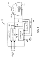
- FIG. 1 is a functional block diagram of a vapor deposition system 100, in accordance with an illustrative embodiment of the invention.
- vapor deposition system 100 is a direct-current (DC) sputtering system.
- DC direct-current
- PVD physical vapor deposition
- the principles of the invention are applicable, without limitation, to DC, alternating-current (AC), pulsed-output, and RF-output processes.
- vapor deposition system 100 includes a coating chamber 105 having an anode 110 and a cathode 115 with which a target 120 is electrically connected.
- target 120 itself serves as cathode 115.
- target 120 serves as anode 110 or is electrically connected with anode 110.
- anode 110 may coincide with the wall of coating chamber 105.
- anode 110 is at ground potential, and the target (cathode) is at negative potential.
- Target 120 and a substrate (or work piece) 125 are disposed within coating chamber 105.
- coating chamber 105 is evacuated, and a noble gas such as Argon (not shown in FIG. 1 ) is introduced into coating chamber 105.
- the gas when "ignited” by electrical energy, becomes a plasma, the positive ions of which bombard target 120, causing atoms of the target material to be knocked free (“sputtered”) and deposited as a film onto substrate 125.
- Vapor deposition system 100 also includes power supply 130. For simplicity, only the relevant functional blocks within power supply 130 have been included in FIG. 1 .
- Power supply 130 includes an input stage (not shown in FIG. 1 ) that receives AC input power from AC line 135. At output 140 of an output stage of power supply 130 (not shown in FIG. 1 ), power supply 130 produces DC output power (P out ). Output 140 is connected to anode 110 and cathode 115 of coating chamber 105.
- AC/DC converter 145 converts AC input power from AC line 135 to DC power for exciting the plasma.
- Controller 150 controls the operation of AC/DC converter 145.
- controller 150 is an embedded computing device that includes a central processing unit (CPU) and memory containing stored program instructions.
- CPU central processing unit
- Controller 150 receives output-current sense line 155, output-voltage sense lines 160, and a user-specified power set point 165 as inputs.
- Control line 170 allows controller 150 to AC/DC converter 145.
- controller 150 may change the duty cycle ratio or switching frequency of AC/DC converter 145.
- a power supply such as power supply 130 is often referred to as a "switch-mode power supply.” Power supply, under control of controller 150, is switched on and off rapidly to control arcing within coating chamber 105.
- controller 150 is configured to detect electrical arcs and to adjust the output current ( I out ) and ⁇ t to deliver substantially the same energy to each detected arc.
- E del is set to be approximately equal to the predetermined E max of the particular target 120.
- controller 150 is configured to remain in a target-conditioning mode until the measured frequency of arcs falls below a predetermined threshold, after which the normal vapor deposition process is resumed.
- controller 150 can detect arcs by, for example, monitoring voltage sense lines 160, current sense line 155, or both.
- controller 150 is configured to switch power supply 130 to a constant current mode, when an arc is detected. This controls the amount of current delivered to the arc during the arc delay time ⁇ t . If the measured arc frequency is above a predetermined threshold, controller 150 is further configured, in this embodiment, to regulate the output current ( I out ) to be inversely proportional to the arc frequency. As explained above, controller 150 is configured to calculate ⁇ t based on the desired E del , I out , and the output voltage ( V out ) by measuring both I out and V out . In a different illustrative embodiment, controller 150 is configured to approximate V out as a constant, in which case only I out needs to be measured.
- FIG. 2 is a flowchart of a method for conditioning a vapor deposition target 120, in accordance with an illustrative embodiment of the invention.
- vapor deposition system 100 is operated using target 120.
- controller 150 detects electrical arcs that occur during the vapor deposition process.
- controller 150 adjusts I out and ⁇ t to deliver more or less the same energy E del to each arc detected at 210.
- E del is approximately equal to E max .
- E max which depends on the material from which target 120 is made and the size of target 120, can be determined by consulting readily available references such as The Handbook of Chemistry and Physics, published by CRC Press , LLC.
- FIG. 3 is a flowchart of a method for controlling a vapor deposition process, in accordance with an illustrative embodiment of the invention.
- vapor deposition system 100 is operated at user-specified output power (set point 165) at 305. If the vapor deposition process is complete at 310, the process terminates at 315. Otherwise, the process proceeds to 320. If controller 150 measures an arc frequency (in units of, e.g., arcs per second) exceeding a predetermined threshold T at 320, vapor deposition system 100 can switch to a target-conditioning mode at 330 in which steps 205, 210, and 215 in FIG.
- arc frequency in units of, e.g., arcs per second
- vapor deposition system 100 may employ normal arc handling in which power supply 130 is switched off for a predetermined period to extinguish an arc.
- the illustrative embodiment shown in FIG. 3 has the advantage of allowing target 120 to be conditioned without the need to vent coating chamber 105 or remove target 120 from coating chamber 105 for physical cleaning.
- FIGS. 4A and 4B are a flowchart of a method for conditioning a vapor deposition target 120, in accordance with another illustrative embodiment of the invention.
- the steps shown in FIGS. 4A and 4B are performed periodically at a predetermined interval. In the particular illustrative embodiment shown, this interval is 100 ms (block 405).
- controller 150 calculates the average arc density (ADAVG) over the previous 100 ms. Controller 150 may average occurrences of arcs sampled every 100 ms over a longer period (e.g., 4-5 seconds) to damp the control loop.
- controller 415 calculates a current limit (ILIM) for power supply 130 as indicated.
- ILIM current limit
- ADTHRESH is a predetermined arc-frequency threshold (e.g., 5-10 arcs/second) used to control whether vapor deposition system 100 operates in target-conditioning mode or normal processing mode.
- ILIMMIN and ILIMMAX are user-provided minimum and maximum output current values, respectively. If ADAVG exceeds ADMAX, ILIM is set to ILIMMIN. In one illustrative embodiment, ADMAX is 250 arcs/second.
- ILIM calculated at 415 exceeds ILIMMAX at 420, ILIM is limited to ILIMMAX at 425. If, on the other hand, ILIM is less than ILIMMIN at 430, ILIM is set to ILIMMIN at 435. At 440, controller 150 applies ILIM to the control loop, and the process proceeds to step 445 in FIG. 4B .
- controller 150 calculates the arc delay time TD as indicated.
- "EARC” in FIG. 4B is the predetermined constant energy to be delivered to each arc.
- EARC is the constant value to which E del is set for each detected arc.
- EARC is approximately equal to E max .
- VARC in FIG. 4B is the output voltage of power supply 130 during the arc delay time TD. In some embodiments, VARC is measured. In other embodiments, VARC is approximated as a predetermined constant.
- controller 150 applies the calculated arc delay time TD to the control loop.
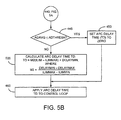
- FIGS. 5A and 5B are a flowchart of a method for conditioning a vapor deposition target 120, in accordance with yet another illustrative embodiment of the invention.
- the output current of power supply 130 would remain the same before and after the onset of an arc.
- a the output current may rise significantly until the arc delay time TD expires and output 140 is shut off for a predetermined period to extinguish the arc.
- the illustrative embodiment shown in FIGS. 5A and 5B adjusts the current limit (ILIM) and arc delay time (TD) so that output 140 of power supply 130 satisfies the objective of delivering substantially the same energy to each arc.
- ILIM current limit
- TD arc delay time
- that constant arc energy is made approximately equal to E max .
- the illustrative embodiment shown in FIGS. 5A and 5B treats the output voltage ( V out ) of power supply 130 as being constant (e.g., 30-50V).
- the product of output current and arc delay time ( I out ⁇ t ) is controlled to be approximately equal to the ratio of the predetermined E del to the known constant output voltage V out . Therefore, this particular illustrative embodiment operates based on I out ⁇ t .
- TD is calculated as indicated in block 505.
- DELAYMIN and DELAYMAX are predetermined minimum and maximum allowable arc delay times, respectively. In one illustrative embodiment, DELAYMIN is 33 ⁇ s, and DELAYMAX is 250 ⁇ s.
- the present invention provides, among other things, a method and system for conditioning a vapor deposition target.
Landscapes
- Chemical & Material Sciences (AREA)
- Engineering & Computer Science (AREA)
- Chemical Kinetics & Catalysis (AREA)
- Materials Engineering (AREA)
- Mechanical Engineering (AREA)
- Metallurgy (AREA)
- Organic Chemistry (AREA)
- Physics & Mathematics (AREA)
- Plasma & Fusion (AREA)
- Analytical Chemistry (AREA)
- Physical Vapour Deposition (AREA)
Claims (18)
- Verfahren zum Konditionieren eines Aufdampfungszielobjekts, umfassend:Betreiben eines Aufdampfungssystems, bei welchem ein Aufdampfungszielobjekt verwendet wird,Erkennen des Auftretens von elektrischen Lichtbögen im Aufdampfungssystem und gekennzeichnet durch Konditionieren des Aufdampfungszielobjekts mittels Anpassung eines Ausgangsstroms einer Stromversorgung, die das Aufdampfungssystem mit Energie versorgt, und mittels Anpassung eines Intervalls, in welchem jedem Lichtbogen Energie zugeführt wird, um im Wesentlichen jedem Lichtbogen die gleiche Energie zuzuführen.
- Verfahren nach Anspruch 1, wobei das Betreiben, Erkennen und Konditionieren solange ausgeführt werden, bis eine gemessene Lichtbogenfrequenz unter einen vorgegebenen Schwellenwerts sinkt.
- Verfahren nach Anspruch 1, wobei die Stromversorgung auf einen konstanten Strommodus umgeschaltet wird, wenn ein Lichtbogen erkannt wird.
- Verfahren nach Anspruch 1, wobei der Ausgangsstrom derart reguliert wird, dass er umgekehrt proportional zu einer gemessenen Lichtbogenfrequenz ist, wenn die gemessene Lichtbogenfrequenz einen vorgegebenen Schwellenwert überschreitet.
- Verfahren nach Anspruch 1, wobei das Anpassen des Intervalls, in welchem jedem Lichtbogen Energie zugeführt wird, umfasst:Messen des Ausgangsstroms und einer Ausgangsspannung der Stromversorgung während einer Lichtbogenverzögerungsdauer undBerechnen des Intervalls, in dem jedem Lichtbogen Energie zugeführt wird, basierend darauf, dass im Wesentlichen jedem Lichtbogen die gleiche Energie zugeführt wird, sowie auf dem gemessenen Ausgangsstrom und der gemessenen Ausgangsspannung.
- Verfahren nach Anspruch 5, wobei während der Lichtbogenverzögerungsdauer die Ausgangsspannung in Form einer vorgegebenen Konstante als Näherungswert verwendet wird, anstatt diese zu messen; und das Intervall, in dem jedem Lichtbogen Energie zugeführt wird, basierend darauf, dass im Wesentlichen jedem Lichtbogen der gleiche Strom zugeführt wird, sowie auf dem gemessene Ausgangsstrom und der angenäherten Ausgangsspannung berechnet wird.
- Verfahren zur Steuerung eines Aufdampfungsprozesses, umfassend:Betreiben des Aufdampfungsprozesses mit einem vom Benutzer definierten Ausgangsleistung, wobei der Aufdampfungsprozess von einer Stromversorgung versorgt wird, undFolgendes ausgeführt wird, wenn die gemessene Lichtbogenfrequenz einen vorgegebenen Schwellenwert überschreitet:Umschalten des Aufdampfungsprozesses in einen Modus der Zielobjektkonditionierung,Erkennen des Auftretens von elektrischen Lichtbögen im Aufdampfungsprozess, gekennzeichnet durch Anpassung eines Ausgangsstroms der Stromversorgung und Anpassung eines Intervalls, in welchem jedem Lichtbogen Energie zugeführt wird, um im Wesentlichen jedem Lichtbogen die gleiche Energie zuzuführen, undWiederholen des Erkennens und Anpassens, bis die gemessene Lichtbogenfrequenz unter den vorgegebenen Schwellenwert fällt.
- Verfahren nach Anspruch 1 oder 7, wobei die jedem Lichtbogen zugeführte Energie ungefähr der maximalen Energie entspricht, der ein in einem Aufdampfungsprozess verwendetes Aufdampfungszielobjekt standhalten kann, ohne dabei beschädigt zu werden.
- Verfahren nach Anspruch 7, ferner umfassend:Wiederaufnehmen des Betriebs des Aufdampfungsprozesses mit vom Benutzer definierter Ausgangsleistung, nachdem die gemessene Lichtbogenfrequenz unter den vorgegebenen Schwellenwerts gefallen ist.
- Verfahren nach Anspruch 7, wobei während des Modus der Zielobjektkonditionierung die Stromversorgung auf einen Stromregulierungsmodus umgeschaltet wird, bei dem der Ausgangsstrom der Stromversorgung im Wesentlichen konstant auf einem vorgegebenen Niveau gehalten wird, ungeachtet dessen, ob ein Lichtbogen vorhanden ist.
- Stromversorgung für ein Aufdampfungssystem, umfassend:eine Eingangsplattform für den Empfang von Eingangsleistung,eine Ausgangsplattform für die Zuführung von Ausgangsleistung zu einem Aufdampfungsprozess,ein Leistungsumwandlungsuntersystem zur Umwandlung vom Eingangsleistung in die Ausgangsleistung undeinen Regler, der mit dem Leistungsumwandlungsuntersystem verbunden ist,wobei der Regler derart konfiguriert ist, dass er während eines Zielobjektkonditionierungsmodus:das Auftreten von elektrischen Lichtbögen im Aufdampfungsprozess erkennt und gekennzeichnet ist durch Anpassung eines Ausgangsstroms der Stromversorgung und Anpassung eines Intervalls, in dem jedem Lichtbogen Energie zugeführt wird, um im Wesentlichen jedem Lichtbogen die gleiche Energie zuzuführen.
- Stromversorgung nach Anspruch 11, wobei die Energie, die laut der Konfiguration des Reglers jedem Lichtbogen zugeführt wird, ungefähr der Maximalenergie entspricht, der ein in einem Aufdampfungsprozess verwendetes Aufdampfungszielobjekt standhalten kann, ohne dabei beschädigt zu werden.
- Stromversorgung nach Anspruch 11, wobei das Leistungsumwandlungsuntersystem Wechselstrom in Gleichstrom umwandelt.
- Stromversorgung nach Anspruch 11, wobei der Regler derart konfiguriert ist, dass er im Zielobjektkonditionierungsmodus verbleibt, bis eine gemessene Lichtbogenfrequenz unter einen vorgegebenen Schwellenwert fällt.
- Stromversorgung nach Anspruch 11, wobei der Regler derart konfiguriert ist, dass die Stromversorgung auf einen konstanten Gleichstrommodus geschaltet wird, wenn ein Lichtbogen erkannt wird.
- Stromversorgung nach Anspruch 11, wobei der Regler derart konfiguriert ist, dass der Ausgangsstrom angepasst wird, damit er umgekehrt proportional zu einer gemessenen Lichtbogenfrequenz ist, wenn die gemessene Lichtbogenfrequenz einen vorgegebenen Schwellenwert überschreitet.
- Stromversorgung nach Anspruch 11, wobei der Regler für Folgendes konfiguriert ist:Messen des Ausgangsstroms und einer Ausgangsspannung der Stromzufuhr während einer Lichtbogenverzögerungsdauer undBerechnen des Intervalls, in welchem jedem Lichtbogen Energie zugeführt wird, basierend darauf, dass im Wesentlichen jedem Lichtbogen die gleiche Energie zugeführt wird, sowie auf dem gemessenen Ausgangsstrom und der gemessenen Ausgangsspannung.
- Stromversorgung nach Anspruch 17, wobei der Regler für Folgendes konfiguriert ist:Annäherung der Ausgangsspannung während der Lichtbogenverzögerungsdauer in Form einer vorgegebenen Konstante undBerechnen des Intervalls, in welchem jedem Lichtbogen Energie zugeführt wird, basierend darauf, dass im Wesentlichen jedem Lichtbogen die gleiche Energie zugeführt geliefert wird, sowie auf dem gemessene Ausgangsstrom und der gemessenen Ausgangsspannung.
Applications Claiming Priority (2)
| Application Number | Priority Date | Filing Date | Title |
|---|---|---|---|
| US11/413,434 US7445695B2 (en) | 2006-04-28 | 2006-04-28 | Method and system for conditioning a vapor deposition target |
| PCT/US2007/067589 WO2007127896A2 (en) | 2006-04-28 | 2007-04-27 | Method and system for conditioning a vapor deposition target |
Publications (3)
| Publication Number | Publication Date |
|---|---|
| EP2013373A2 EP2013373A2 (de) | 2009-01-14 |
| EP2013373A4 EP2013373A4 (de) | 2010-05-26 |
| EP2013373B1 true EP2013373B1 (de) | 2011-08-31 |
Family
ID=38647307
Family Applications (1)
| Application Number | Title | Priority Date | Filing Date |
|---|---|---|---|
| EP07761416A Active EP2013373B1 (de) | 2006-04-28 | 2007-04-27 | Verfahren und system zur aufbereitung eines aufdampfungsziels |
Country Status (7)
| Country | Link |
|---|---|
| US (2) | US7445695B2 (de) |
| EP (1) | EP2013373B1 (de) |
| JP (1) | JP2009535506A (de) |
| KR (1) | KR101104778B1 (de) |
| CN (1) | CN101466861A (de) |
| TW (1) | TW200848538A (de) |
| WO (1) | WO2007127896A2 (de) |
Families Citing this family (26)
| Publication number | Priority date | Publication date | Assignee | Title |
|---|---|---|---|---|
| DE102004015090A1 (de) | 2004-03-25 | 2005-11-03 | Hüttinger Elektronik Gmbh + Co. Kg | Bogenentladungserkennungseinrichtung |
| DE502005006550D1 (de) * | 2005-12-22 | 2009-03-12 | Huettinger Elektronik Gmbh | Verfahren und Vorrichtung zur Arcerkennung in einem Plasmaprozess |
| US7445695B2 (en) * | 2006-04-28 | 2008-11-04 | Advanced Energy Industries Inc. | Method and system for conditioning a vapor deposition target |
| US7741825B2 (en) * | 2006-11-02 | 2010-06-22 | Infineon Technologies Ag | Power supply circuit with temperature-dependent drive signal |
| DE502006005363D1 (de) * | 2006-11-23 | 2009-12-24 | Huettinger Elektronik Gmbh | Verfahren zum Erkennen einer Bogenentladung in einem Plasmaprozess und Bogenentladungserkennungsvorrichtung |
| US7795817B2 (en) * | 2006-11-24 | 2010-09-14 | Huettinger Elektronik Gmbh + Co. Kg | Controlled plasma power supply |
| EP1928009B1 (de) * | 2006-11-28 | 2013-04-10 | HÜTTINGER Elektronik GmbH + Co. KG | Bogenentladungs-Erkennungseinrichtung, Plasma-Leistungsversorgung und Verfahren zum Erkennen von Bogenentladungen |
| DE502006009308D1 (de) * | 2006-12-14 | 2011-05-26 | Huettinger Elektronik Gmbh | Bogenentladungs-Erkennungseinrichtung, Plasma-Leistungsversorgung und Verfahren zum Erkennen von Bogenentladungen |
| EP1978542B1 (de) | 2007-03-08 | 2010-12-29 | HÜTTINGER Elektronik GmbH + Co. KG | Verfahren und Vorrichtung zum Unterdrücken von Bogenentladungen beim Betreiben eines Plasmaprozesses |
| ATE547804T1 (de) * | 2007-12-24 | 2012-03-15 | Huettinger Electronic Sp Z O O | Stromänderungsbegrenzungsvorrichtung |
| US8044594B2 (en) * | 2008-07-31 | 2011-10-25 | Advanced Energy Industries, Inc. | Power supply ignition system and method |
| US8815329B2 (en) * | 2008-12-05 | 2014-08-26 | Advanced Energy Industries, Inc. | Delivered energy compensation during plasma processing |
| EP2648209B1 (de) | 2009-02-17 | 2018-01-03 | Solvix GmbH | Energieversorgungsvorrichtung zur Plasmaverarbeitung |
| US20100252047A1 (en) | 2009-04-03 | 2010-10-07 | Kirk Seth M | Remote fluorination of fibrous filter webs |
| US11978611B2 (en) | 2009-05-01 | 2024-05-07 | Advanced Energy Industries, Inc. | Apparatus with switches to produce a waveform |
| US11615941B2 (en) | 2009-05-01 | 2023-03-28 | Advanced Energy Industries, Inc. | System, method, and apparatus for controlling ion energy distribution in plasma processing systems |
| JP5363281B2 (ja) * | 2009-11-25 | 2013-12-11 | 株式会社アルバック | 電源装置 |
| US20110143049A1 (en) * | 2009-12-16 | 2011-06-16 | Xing-Cai Guo | Lubricant removal to reuse disks for conditioning deposition tools |
| DE102010031568B4 (de) | 2010-07-20 | 2014-12-11 | TRUMPF Hüttinger GmbH + Co. KG | Arclöschanordnung und Verfahren zum Löschen von Arcs |
| US9685297B2 (en) | 2012-08-28 | 2017-06-20 | Advanced Energy Industries, Inc. | Systems and methods for monitoring faults, anomalies, and other characteristics of a switched mode ion energy distribution system |
| EP3054472A1 (de) * | 2015-02-03 | 2016-08-10 | TRUMPF Huettinger Sp. Z o. o. | Lichtbogenbehandlungsvorrichtung und Verfahren dazu |
| CN110643964B (zh) * | 2019-09-24 | 2022-06-14 | 北京北方华创微电子装备有限公司 | 磁控溅射工艺中直流电源的控制方法、控制装置及系统 |
| EP4053304A1 (de) * | 2021-03-01 | 2022-09-07 | Bühler Alzenau GmbH | Beschichter-konditionierungsmodus |
| TWI820472B (zh) * | 2021-08-19 | 2023-11-01 | 天虹科技股份有限公司 | 物理氣相沉積腔體的暖機方法 |
| CN115707791A (zh) * | 2021-08-19 | 2023-02-21 | 鑫天虹(厦门)科技有限公司 | 物理气相沉积机台的暖机方法 |
| US12567572B2 (en) | 2023-07-11 | 2026-03-03 | Advanced Energy Industries, Inc. | Plasma behaviors predicted by current measurements during asymmetric bias waveform application |
Family Cites Families (14)
| Publication number | Priority date | Publication date | Assignee | Title |
|---|---|---|---|---|
| US5718813A (en) | 1992-12-30 | 1998-02-17 | Advanced Energy Industries, Inc. | Enhanced reactive DC sputtering system |
| SG74667A1 (en) | 1993-07-28 | 2000-08-22 | Asahi Glass Co Ltd | Method of an apparatus for sputtering |
| US5651865A (en) | 1994-06-17 | 1997-07-29 | Eni | Preferential sputtering of insulators from conductive targets |
| WO1996031899A1 (en) | 1995-04-07 | 1996-10-10 | Advanced Energy Industries, Inc. | Adjustable energy quantum thin film plasma processing system |
| CN1223698C (zh) | 1997-02-20 | 2005-10-19 | 芝浦机械电子装置股份有限公司 | 用于溅射的电源装置和使用该装置的溅射设备 |
| KR100539612B1 (ko) | 1997-02-28 | 2006-03-20 | 도소 가부시키가이샤 | 스퍼터링타겟제조방법 |
| US5993615A (en) | 1997-06-19 | 1999-11-30 | International Business Machines Corporation | Method and apparatus for detecting arcs |
| DE19740793C2 (de) | 1997-09-17 | 2003-03-20 | Bosch Gmbh Robert | Verfahren zur Beschichtung von Oberflächen mittels einer Anlage mit Sputterelektroden und Verwendung des Verfahrens |
| JP2000100790A (ja) | 1998-09-22 | 2000-04-07 | Canon Inc | プラズマ処理装置及びそれを用いた処理方法 |
| US6451389B1 (en) | 1999-04-17 | 2002-09-17 | Advanced Energy Industries, Inc. | Method for deposition of diamond like carbon |
| US6736944B2 (en) | 2002-04-12 | 2004-05-18 | Schneider Automation Inc. | Apparatus and method for arc detection |
| US7247221B2 (en) | 2002-05-17 | 2007-07-24 | Applied Films Corporation | System and apparatus for control of sputter deposition process |
| TW574385B (en) | 2002-06-25 | 2004-02-01 | Hannstar Display Corp | Method of pre-sputtering with an increased rate of use of sputtering target |
| US7445695B2 (en) * | 2006-04-28 | 2008-11-04 | Advanced Energy Industries Inc. | Method and system for conditioning a vapor deposition target |
-
2006
- 2006-04-28 US US11/413,434 patent/US7445695B2/en active Active
-
2007
- 2007-04-27 KR KR1020087028729A patent/KR101104778B1/ko active Active
- 2007-04-27 WO PCT/US2007/067589 patent/WO2007127896A2/en not_active Ceased
- 2007-04-27 JP JP2009507976A patent/JP2009535506A/ja not_active Withdrawn
- 2007-04-27 EP EP07761416A patent/EP2013373B1/de active Active
- 2007-04-27 CN CNA2007800196320A patent/CN101466861A/zh active Pending
- 2007-06-11 TW TW096121076A patent/TW200848538A/zh unknown
-
2008
- 2008-09-17 US US12/212,506 patent/US8357266B2/en active Active
Also Published As
| Publication number | Publication date |
|---|---|
| US20090008240A1 (en) | 2009-01-08 |
| US8357266B2 (en) | 2013-01-22 |
| WO2007127896A2 (en) | 2007-11-08 |
| TW200848538A (en) | 2008-12-16 |
| CN101466861A (zh) | 2009-06-24 |
| EP2013373A4 (de) | 2010-05-26 |
| WO2007127896A3 (en) | 2008-10-30 |
| EP2013373A2 (de) | 2009-01-14 |
| US20070251813A1 (en) | 2007-11-01 |
| KR20090005396A (ko) | 2009-01-13 |
| US7445695B2 (en) | 2008-11-04 |
| JP2009535506A (ja) | 2009-10-01 |
| KR101104778B1 (ko) | 2012-01-12 |
Similar Documents
| Publication | Publication Date | Title |
|---|---|---|
| EP2013373B1 (de) | Verfahren und system zur aufbereitung eines aufdampfungsziels | |
| US8658001B2 (en) | Method and control system for depositing a layer | |
| US5300205A (en) | Method and device for treating substrates | |
| EP0692138B2 (de) | Reaktives gleichstrom-zerstäubungssystem | |
| US9039871B2 (en) | Methods and apparatus for applying periodic voltage using direct current | |
| CN100510164C (zh) | 用于控制溅射沉积过程的方法和装置 | |
| EP2314136B1 (de) | Stromversorgungsaktivierungssystem und -verfahren | |
| JP4714166B2 (ja) | 基板のプラズマ処理装置及びプラズマ処理方法 | |
| KR101749766B1 (ko) | 플라즈마 처리 방법 및 플라즈마 처리 장치 | |
| US20090127101A1 (en) | Methods and apparatus for sputtering deposition using direct current | |
| Audronis et al. | Control of reactive high power impulse magnetron sputtering processes | |
| WO1996031899A1 (en) | Adjustable energy quantum thin film plasma processing system | |
| JP2758999B2 (ja) | 真空アーク蒸着装置 | |
| US10566177B2 (en) | Pulse shape controller for sputter sources | |
| US10407767B2 (en) | Method for depositing a layer using a magnetron sputtering device | |
| Carter et al. | Parameter optimization in pulsed DC reactive sputter deposition of aluminum oxide | |
| KR100584168B1 (ko) | 플라즈마 공정용 전원 장치 및 전원 공급 방법 | |
| Wiatrowski et al. | Pulsed-DC selfsputtering of copper | |
| Bandorf et al. | Modifications of coatings by DC-sputtering with superimposed HPPMS | |
| JP2007031815A (ja) | プレーナマグネトロンスパッタ装置およびプレーナマグネトロンスパッタ成膜方法 | |
| Gajewski et al. | „Newest achievements with bipolar power supplies in dual magnetron processes,” | |
| JP2000345341A (ja) | 反応性スパッタリング方法 |
Legal Events
| Date | Code | Title | Description |
|---|---|---|---|
| PUAI | Public reference made under article 153(3) epc to a published international application that has entered the european phase |
Free format text: ORIGINAL CODE: 0009012 |
|
| 17P | Request for examination filed |
Effective date: 20081024 |
|
| AK | Designated contracting states |
Kind code of ref document: A2 Designated state(s): AT BE BG CH CY CZ DE DK EE ES FI FR GB GR HU IE IS IT LI LT LU LV MC MT NL PL PT RO SE SI SK TR |
|
| AX | Request for extension of the european patent |
Extension state: AL BA HR MK RS |
|
| DAX | Request for extension of the european patent (deleted) | ||
| RBV | Designated contracting states (corrected) |
Designated state(s): DE GB |
|
| A4 | Supplementary search report drawn up and despatched |
Effective date: 20100428 |
|
| RIC1 | Information provided on ipc code assigned before grant |
Ipc: C23C 14/34 20060101AFI20081111BHEP Ipc: C23C 14/54 20060101ALI20100422BHEP |
|
| GRAP | Despatch of communication of intention to grant a patent |
Free format text: ORIGINAL CODE: EPIDOSNIGR1 |
|
| RIC1 | Information provided on ipc code assigned before grant |
Ipc: C23C 14/34 20060101AFI20110302BHEP Ipc: C23C 14/54 20060101ALI20110302BHEP |
|
| GRAS | Grant fee paid |
Free format text: ORIGINAL CODE: EPIDOSNIGR3 |
|
| GRAA | (expected) grant |
Free format text: ORIGINAL CODE: 0009210 |
|
| AK | Designated contracting states |
Kind code of ref document: B1 Designated state(s): DE GB |
|
| REG | Reference to a national code |
Ref country code: GB Ref legal event code: FG4D |
|
| REG | Reference to a national code |
Ref country code: DE Ref legal event code: R096 Ref document number: 602007016800 Country of ref document: DE Effective date: 20111103 |
|
| PLBE | No opposition filed within time limit |
Free format text: ORIGINAL CODE: 0009261 |
|
| STAA | Information on the status of an ep patent application or granted ep patent |
Free format text: STATUS: NO OPPOSITION FILED WITHIN TIME LIMIT |
|
| 26N | No opposition filed |
Effective date: 20120601 |
|
| REG | Reference to a national code |
Ref country code: DE Ref legal event code: R097 Ref document number: 602007016800 Country of ref document: DE Effective date: 20120601 |
|
| PGFP | Annual fee paid to national office [announced via postgrant information from national office to epo] |
Ref country code: GB Payment date: 20130424 Year of fee payment: 7 |
|
| GBPC | Gb: european patent ceased through non-payment of renewal fee |
Effective date: 20140427 |
|
| PG25 | Lapsed in a contracting state [announced via postgrant information from national office to epo] |
Ref country code: GB Free format text: LAPSE BECAUSE OF NON-PAYMENT OF DUE FEES Effective date: 20140427 |
|
| REG | Reference to a national code |
Ref country code: DE Ref legal event code: R082 Ref document number: 602007016800 Country of ref document: DE Representative=s name: FIENER, JOSEF, DE Ref country code: DE Ref legal event code: R081 Ref document number: 602007016800 Country of ref document: DE Owner name: AES GLOBAL HOLDINGS, PTE, LTD., SG Free format text: FORMER OWNER: ADVANCED ENERGY INDUSTRIES, INC., FORT COLLINS, COL., US Ref country code: DE Ref legal event code: R081 Ref document number: 602007016800 Country of ref document: DE Owner name: AES GLOBAL HOLDINGS, PTE. LTD., SG Free format text: FORMER OWNER: ADVANCED ENERGY INDUSTRIES, INC., FORT COLLINS, COL., US Ref country code: DE Ref legal event code: R082 Ref document number: 602007016800 Country of ref document: DE Representative=s name: STOLMAR & PARTNER PATENTANWAELTE PARTG MBB, DE |
|
| REG | Reference to a national code |
Ref country code: DE Ref legal event code: R082 Ref document number: 602007016800 Country of ref document: DE Representative=s name: FIENER, JOSEF, DE Ref country code: DE Ref legal event code: R081 Ref document number: 602007016800 Country of ref document: DE Owner name: AES GLOBAL HOLDINGS, PTE. LTD., SG Free format text: FORMER OWNER: AES GLOBAL HOLDINGS, PTE, LTD., SINGAPORE, SG Ref country code: DE Ref legal event code: R082 Ref document number: 602007016800 Country of ref document: DE Representative=s name: STOLMAR & PARTNER PATENTANWAELTE PARTG MBB, DE |
|
| REG | Reference to a national code |
Ref country code: DE Ref legal event code: R082 Ref document number: 602007016800 Country of ref document: DE Representative=s name: STOLMAR & PARTNER PATENTANWAELTE PARTG MBB, DE |
|
| P01 | Opt-out of the competence of the unified patent court (upc) registered |
Effective date: 20230911 |
|
| PGFP | Annual fee paid to national office [announced via postgrant information from national office to epo] |
Ref country code: DE Payment date: 20250305 Year of fee payment: 19 |