EP2014137B1 - Dispositif électroluminescent organique présentant un motif électroluminescent et procédé de préparation dudit dispositif - Google Patents
Dispositif électroluminescent organique présentant un motif électroluminescent et procédé de préparation dudit dispositif Download PDFInfo
- Publication number
- EP2014137B1 EP2014137B1 EP07746338.8A EP07746338A EP2014137B1 EP 2014137 B1 EP2014137 B1 EP 2014137B1 EP 07746338 A EP07746338 A EP 07746338A EP 2014137 B1 EP2014137 B1 EP 2014137B1
- Authority
- EP
- European Patent Office
- Prior art keywords
- functions
- light emitting
- organic material
- layers
- predetermined pattern
- Prior art date
- Legal status (The legal status is an assumption and is not a legal conclusion. Google has not performed a legal analysis and makes no representation as to the accuracy of the status listed.)
- Active
Links
- RLDLOQGMDUWGDM-UHFFFAOYSA-N CC(C(C=C1[N+]([O-])=O)c2nc(c3nc(-c(cc4[N+]([O-])=O)ccc4[N+]([O-])=O)c(-c(cc4[N+]([O-])=O)ccc4[N+]([O-])=O)nc3c3nc(-c(cc4[N+]([O-])=O)ccc4[N+]([O-])=O)c(-c(cc4[N+]([O-])=O)ccc4[N+]([O-])=O)nc33)c3nc2-c(cc2[N+]([O-])=O)ccc2[N+]([O-])=O)C=C1[N+]([O-])=O Chemical compound CC(C(C=C1[N+]([O-])=O)c2nc(c3nc(-c(cc4[N+]([O-])=O)ccc4[N+]([O-])=O)c(-c(cc4[N+]([O-])=O)ccc4[N+]([O-])=O)nc3c3nc(-c(cc4[N+]([O-])=O)ccc4[N+]([O-])=O)c(-c(cc4[N+]([O-])=O)ccc4[N+]([O-])=O)nc33)c3nc2-c(cc2[N+]([O-])=O)ccc2[N+]([O-])=O)C=C1[N+]([O-])=O RLDLOQGMDUWGDM-UHFFFAOYSA-N 0.000 description 1
- 0 Cc1cc(S(c(nc(c2c(c(c3n4)nc(S(c5ccccc5)(=O)=O)c4S(c4ccccc4)(=O)=O)nc(*c4ccccc4)c(S(c4ccccc4)(=O)=O)n2)c3n2)c2S(c2ccccc2)(=O)=O)(=O)=O)ccc1 Chemical compound Cc1cc(S(c(nc(c2c(c(c3n4)nc(S(c5ccccc5)(=O)=O)c4S(c4ccccc4)(=O)=O)nc(*c4ccccc4)c(S(c4ccccc4)(=O)=O)n2)c3n2)c2S(c2ccccc2)(=O)=O)(=O)=O)ccc1 0.000 description 1
Images


Classifications
-
- C—CHEMISTRY; METALLURGY
- C09—DYES; PAINTS; POLISHES; NATURAL RESINS; ADHESIVES; COMPOSITIONS NOT OTHERWISE PROVIDED FOR; APPLICATIONS OF MATERIALS NOT OTHERWISE PROVIDED FOR
- C09K—MATERIALS FOR MISCELLANEOUS APPLICATIONS, NOT PROVIDED FOR ELSEWHERE
- C09K11/00—Luminescent materials, e.g. electroluminescent or chemiluminescent
- C09K11/06—Luminescent materials, e.g. electroluminescent or chemiluminescent containing organic luminescent materials
-
- H—ELECTRICITY
- H05—ELECTRIC TECHNIQUES NOT OTHERWISE PROVIDED FOR
- H05B—ELECTRIC HEATING; ELECTRIC LIGHT SOURCES NOT OTHERWISE PROVIDED FOR; CIRCUIT ARRANGEMENTS FOR ELECTRIC LIGHT SOURCES, IN GENERAL
- H05B33/00—Electroluminescent light sources
- H05B33/12—Light sources with substantially two-dimensional [2D] radiating surfaces
- H05B33/14—Light sources with substantially two-dimensional [2D] radiating surfaces characterised by the chemical or physical composition or the arrangement of the electroluminescent material, or by the simultaneous addition of the electroluminescent material in or onto the light source
-
- H—ELECTRICITY
- H10—SEMICONDUCTOR DEVICES; ELECTRIC SOLID-STATE DEVICES NOT OTHERWISE PROVIDED FOR
- H10K—ORGANIC ELECTRIC SOLID-STATE DEVICES
- H10K50/00—Organic light-emitting devices
- H10K50/10—OLEDs or polymer light-emitting diodes [PLED]
- H10K50/17—Carrier injection layers
-
- H—ELECTRICITY
- H10—SEMICONDUCTOR DEVICES; ELECTRIC SOLID-STATE DEVICES NOT OTHERWISE PROVIDED FOR
- H10K—ORGANIC ELECTRIC SOLID-STATE DEVICES
- H10K50/00—Organic light-emitting devices
- H10K50/80—Constructional details
- H10K50/805—Electrodes
-
- H—ELECTRICITY
- H10—SEMICONDUCTOR DEVICES; ELECTRIC SOLID-STATE DEVICES NOT OTHERWISE PROVIDED FOR
- H10K—ORGANIC ELECTRIC SOLID-STATE DEVICES
- H10K59/00—Integrated devices, or assemblies of multiple devices, comprising at least one organic light-emitting element covered by group H10K50/00
- H10K59/10—OLED displays
- H10K59/221—Static displays, e.g. displaying permanent logos
-
- H—ELECTRICITY
- H10—SEMICONDUCTOR DEVICES; ELECTRIC SOLID-STATE DEVICES NOT OTHERWISE PROVIDED FOR
- H10K—ORGANIC ELECTRIC SOLID-STATE DEVICES
- H10K71/00—Manufacture or treatment specially adapted for the organic devices covered by this subclass
- H10K71/20—Changing the shape of the active layer in the devices, e.g. patterning
- H10K71/211—Changing the shape of the active layer in the devices, e.g. patterning by selective transformation of an existing layer
-
- H—ELECTRICITY
- H10—SEMICONDUCTOR DEVICES; ELECTRIC SOLID-STATE DEVICES NOT OTHERWISE PROVIDED FOR
- H10K—ORGANIC ELECTRIC SOLID-STATE DEVICES
- H10K71/00—Manufacture or treatment specially adapted for the organic devices covered by this subclass
- H10K71/621—Providing a shape to conductive layers, e.g. patterning or selective deposition
-
- C—CHEMISTRY; METALLURGY
- C09—DYES; PAINTS; POLISHES; NATURAL RESINS; ADHESIVES; COMPOSITIONS NOT OTHERWISE PROVIDED FOR; APPLICATIONS OF MATERIALS NOT OTHERWISE PROVIDED FOR
- C09K—MATERIALS FOR MISCELLANEOUS APPLICATIONS, NOT PROVIDED FOR ELSEWHERE
- C09K2211/00—Chemical nature of organic luminescent or tenebrescent compounds
- C09K2211/10—Non-macromolecular compounds
- C09K2211/1018—Heterocyclic compounds
- C09K2211/1025—Heterocyclic compounds characterised by ligands
- C09K2211/1044—Heterocyclic compounds characterised by ligands containing two nitrogen atoms as heteroatoms
-
- H—ELECTRICITY
- H10—SEMICONDUCTOR DEVICES; ELECTRIC SOLID-STATE DEVICES NOT OTHERWISE PROVIDED FOR
- H10K—ORGANIC ELECTRIC SOLID-STATE DEVICES
- H10K71/00—Manufacture or treatment specially adapted for the organic devices covered by this subclass
-
- H—ELECTRICITY
- H10—SEMICONDUCTOR DEVICES; ELECTRIC SOLID-STATE DEVICES NOT OTHERWISE PROVIDED FOR
- H10K—ORGANIC ELECTRIC SOLID-STATE DEVICES
- H10K85/00—Organic materials used in the body or electrodes of devices covered by this subclass
- H10K85/60—Organic compounds having low molecular weight
- H10K85/649—Aromatic compounds comprising a hetero atom
- H10K85/657—Polycyclic condensed heteroaromatic hydrocarbons
- H10K85/6572—Polycyclic condensed heteroaromatic hydrocarbons comprising only nitrogen in the heteroaromatic polycondensed ring system, e.g. phenanthroline or carbazole
-
- H—ELECTRICITY
- H10—SEMICONDUCTOR DEVICES; ELECTRIC SOLID-STATE DEVICES NOT OTHERWISE PROVIDED FOR
- H10K—ORGANIC ELECTRIC SOLID-STATE DEVICES
- H10K85/00—Organic materials used in the body or electrodes of devices covered by this subclass
- H10K85/731—Liquid crystalline materials
Definitions
- the present invention relates to an organic light emitting device, and a method for producing the same. More particularly, the present invention pertains to an organic light emitting device having a light emitting pattern, and a method for producing the same.
- An organic light emitting device includes two electrodes and an organic material layer that is interposed between the electrodes, and electrons and holes are injected from two electrodes to the organic material layer, so that a current is converted into visible rays to emit light.
- FIG. 1 is a sectional view of a conventional organic light emitting device.
- the organic light emitting device includes a light emitting layer 50 that is interposed between two electrodes, for example, an anode electrode 20 and a cathode electrode 70. Any one of the two electrodes, for example, the anode electrode 20, is provided on a transparent substrate 10, and light that is emitted from the light emitting layer 50 passes therethrough.
- the organic light emitting device may further comprise one or more layers that are selected from the group consisting of an electron injecting layer 65, an electron transporting layer 60, a hole transporting layer 45, and a hole injecting layer 40 in order to improve performance.
- the organic light emitting device may further include an insulating layer 30 having a predetermined pattern on an electrode on the transparent substrate 10 to separate a light emitting region A) and a non-light emitting region B).
- US2004/077250 A1 discloses an organic light emitting device comprising an organic multilayer stack which can be patterned by direct exposure to ultraviolet light.
- DLP digital light processing
- the present invention provides a method of producing an organic light emitting device according to the independent method claim 1.
- the changing of the functions of the predetermined pattern regions of one or more layers of the organic material layers may be performed by using DLP (digital light processing).
- the present invention provides an organic light emitting device according to the independent apparatus claim 9.
- An organic light emitting device includes a layer that has a partially or wholly changed function in a region corresponding to a predetermined pattern. Thereby, it is possible to easily produce the organic light emitting device that emits light in a predetermined pattern. It is unnecessary to use an additional device to emit light in the pattern, a production process may be simple, and there is an advantage in terms of cost. In particular, in the case of when DLP is used to change the function, it is possible to more easily realize a gray scale and more finely and precisely control the gray scale as compared to the case of when an organic light emitting device that emits light in a predetermined pattern by using a photomask and the like is produced.
- a method of producing an organic light emitting device includes changing functions of predetermined pattern regions of one or more layers of an organic material layer in the device so that the organic light emitting device can emit light in a predetermined pattern.
- a step of changing the functions of predetermined pattern regions of one or more layers of the organic material layer may be a step of providing an additional function to the region having the changed function so that the region corresponds to a light emitting region of the organic light emitting device or removing a function from the region so that the region corresponds to a non-light emitting region.
- the above-mentioned step is performed so that functions of a predetermined pattern region and the other regions in one or more layers constituting the organic light emitting device are different from each other and the layer containing the regions having the different functions affects the light emitting pattern of the organic light emitting device to force the organic light emitting device to emit light in the predetermined pattern.
- the layer in which the function of the predetermined pattern region is changed is the organic material layer.
- the layer in which the function of the predetermined pattern region is changed is a charge transporting layer, for example, a layer that injects and/or transports a hole
- charge transporting efficiencies of the predetermined pattern region and the other regions are different from each other. Due to a difference in charge transporting efficiency into the light emitting layer, light is emitted from the light emitting layer according to the light emitting pattern that corresponds to the predetermined pattern region of the charge transporting layer.
- the organic light emitting device that is produced by using a method of producing the organic light emitting device according to the present invention does not include layers other than the layers constituting the organic light emitting device, problems such as deterioration in interlayer interface properties and reduction in light emitting efficiency that may occur when the layers other than the layers constituting the organic light emitting device are provided like the known process may be prevented.
- light emission is 0% and 100% at a portion where the insulating layer is formed and at another portion where the insulating layer is not formed, respectively.
- the light emitting pattern is obtained only by using an on/off form.
- the degree of the changing of the functions of the predetermined pattern regions of one or more layers constituting the organic light emitting device is controlled to form a light emitting pattern having a gray scale in which light emission gradually changes from a high light emitting portion via a medium light emitting portion to a low emitting portion, that is, a desirable gradation, as well as an on/off type light emitting pattern.
- the layer in which the function of the predetermined pattern region is changed is one or more layers of the organic material layer.
- the organic material layer in which the function of the predetermined pattern region is changed may be one or more layers selected from a hole injecting and a hole transporting, or a layer having two or more functions among the functions of the above-mentioned layers.
- the organic material layer may be a layer that is additionally formed not to provide the functions but to form the light emitting pattern according to the purpose of the present invention.
- the organic material layer be a layer for performing charge transportation, for example, hole or hole transportation.
- a process of changing the functions of the predetermined pattern regions of one or more layers of the organic material layer is not limited as long as the purpose is achieved.
- the process may be performed by means of an optical process, for example processes using UV, a laser, or an e-beam.
- the functions of the predetermined pattern regions may be finely changed.
- the mechanism of the DLP is as follows.
- the DLP is short for digital light processing and developed by researchers of Texas Instruments, Inc. in the year 1987.
- an image is processed by using a DMD (digital micromirror device).
- the DMD may include 750,000 or more micromirrors. Since an image is shown by using the reflecting mirrors, there are advantages in that light efficiency is excellent and a fine image can be obtained.
- a digital configuration is advantageous in that a desired image can be precisely obtained with high reliability as compared to an analog configuration and products have a small size and are light in weight.
- a digital image is a combination of many 0 and 1 signals.
- a DMD module that is the kernel of the DLP technology may be operated according to the combination of the digital signals.
- the combination of digital image signals that are transmitted from video memories or video processors is expressed by operation of the micromirrors constituting the DMD.
- each of the micromirrors of the DMD module may have the shape of a square having the size of 16 x 16 micrometers (microns), and an interval between the micromirrors may be less than 1 micrometer and the micromirrors may be very densely disposed. Both edges of each of the micromirrors that are contained in the DMD module used to perform the DLP are moved by using the digital signals of 0 and 1 to express digital image signals. Each of the micromirrors may rotate right and left by, for example, 0 to 10°, and the digital image signals that are saved in video memories are transmitted to driving apparatuses of the micromirrors to operate the micromirrors.
- the rotation of the mirrors is expressed by the fine pixels, and the light and the shade of the pixels are expressed based on the above-mentioned mechanism.
- the micromirrors that constitute the DMD module used to perform DLP are illustrated in Fig. 6 .
- the size and the rotation angle of the micromirror are given to illustrate, but are not to be construed to limit the present invention.
- the DLP is performed according to a mechanism that is similar to that of a card section in a sports stadium.
- a whole image is expressed by using movement of boards.
- boards are formed of mirrors and, when rays are radiated from a light source at a predetermined position in a predetermined direction, the rays reflect by movement of the mirrors and lens portions through which the rays penetrate and the other portions through which the rays cannot penetrate form a single image.
- a gray tone color sense needs to be expressed in addition to the white and black colors.
- the color sense may be expressed by using the mechanism of the card section of 0 and 1 that are changed several thousands times per one second. For example, when the DMD mirrors are to be moved 1000 times per unit time, if a frequency of 0 and 1 is finely controlled by using the mirrors, it is possible to very precisely control color tones of pixels.
- a movement speed of the micromirror of the DMD may be set to 500,000 or more times per second. Thereby, the light and the shade of black and white colors are expressed and a gray scale image may be outputted by using a digital configuration.
- an energy source may be selectively applied to an organic material layer, so that the function of the predetermined pattern region of the organic material layer is selectively changed.
- the organic material layer in which the function is capable of being changed by using the above-mentioned optical method is a layer that includes the compound represented by Formula 1.
- the compound of Formula 1 may function to inject and/or transport a hole in the organic light emitting device, but the injecting and/ or transporting functions of the region that is treated by the above-mentioned optical method may be partially or totally removed.
- Fig. 7 is a graph illustrating change of the function of the organic material layer including the compound of Formula 1 according to radiation of UV.
- R 1 to R 6 are each selected from the group consisting of hydrogen, a halogen atom, nitrile (-CN), nitro (-NO 2 ), sulfonyl (-SO 2 R), sulfoxide (-SOR), sulfonamide (-SO 2 NR), sulfonate (-SO 3 R), trifluoromethyl (-CF 3 ), ester (-COOR), amide (-CONHR or -CONRR'), substituted or unsubstituted straight- or branched-chained C 1 -C 12 alkoxy, substituted or unsubstituted straight- or branched-chained C 1 -C 12 alkyl, a substituted or unsubstituted aromatic or nonaromatic hetero ring, substituted or unsubstituted aryl, substituted or unsubstituted mono- or di-arylamine, and substituted or unsubstituted aralkylamine, and R and R' are each
- the compound of Formula 1 may be selected from the compounds represented by Formulae 1-1 to 1-6.
- the step of changing the functions of the predetermined pattern regions of one or more layers of the organic material layer may be performed after the other organic material layers are formed or after the second electrode is formed, as long as it is performed after the layer in which the function of the predetermined pattern region is changed is formed.
- the step is performed after the layer in which the functions of the predetermined pattern regions are to be changed is formed and before the other organic material layers or the second electrodes are formed.
- the step of changing the functions of the predetermined pattern regions of one or more layers of the organic material layer may be performed so that the organic light emitting device realizes on/off or various types of light emitting gradations by controlling the degree of the changing of the functions according to the position of the pattern region, for example, by controlling exposure in the case of when the optical method is used.
- all of the functions of the predetermined pattern regions are changed to form a light emitting pattern so that the intensity of emitted light is expressed by an on/off form at the region where the functions are changed and the region where the functions are not changed.
- exposure may be controlled according to the position of the pattern region so that the degree of changing of the functions varies, thus forming the light emitting pattern having two different intensities of emitted light.
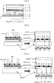
- Figs. 2 and 3 An example relating to this is illustrated in Figs. 2 and 3 .
- UV is radiated on the non-light emitting region to completely remove the function of the region, so that the produced organic light emitting device displays two intensities of emitted light of the light emitting region A and the non-light emitting region B, that is, on/off intensities.
- Fig. 3 photomasks that are capable of controlling radiation of UV according to the position of regions are used.
- the degree of changing of the functions of the pattern regions varies so that the organic light emitting device has various types of light emitting intensities.
- Fig. 2 UV is radiated on the non-light emitting region to completely remove the function of the region, so that the produced organic light emitting device displays two intensities of emitted light of the light emitting region A and the non-light emitting region B, that is, on/off intensities.
- photomasks that are capable of controlling radiation of UV according to the position of regions are used.
- the step of changing the functions of the pattern regions may be performed through a single stage or through multiple stages to change at least a portion of functions of the different pattern regions.
- photomasks having various types of materials or thicknesses may be used or exposure may be controlled to adjust exposure according to the type of region.
- a photomask that is made of various types of materials or has various thicknesses and is capable of controlling permeation of light according to the region may be used, a plurality of photomasks that is made of various types of materials or has various thicknesses may be used, or a light source that is capable of controlling radiation of light according to the region may be used.
- Fig. 5 illustrates the change in function that is controlled by using the DLP.
- the controlling is performed based on the above mechanism.
- all of the functions of the predetermined pattern regions may be changed to ensure the light emitting pattern where the intensity of emitted light is expressed in the on/off form at the region where the functions are changed and at the region where the functions are not changed.
- exposure may be controlled according to the type of region so that the degree of the changing of the functions varies. Thereby, it is possible to ensure the light emitting pattern so that two or more different intensities of emitted light are obtained.
- the organic light emitting device may be produced by using a typical method of producing an organic light emitting device and a typical material, except that the functions of the predetermined pattern regions of one or more constituent layers are changed.
- metal or metal oxide having conductivity or an alloy thereof is deposited on a substrate by using a PVD (physical vapor deposition) process such as sputtering or e-beam evaporation to form an anode, an organic material layer that includes a hole injecting layer, a hole transporting layer, a light emitting layer, and an electron transporting layer is formed, and a material that is capable of being used to form a cathode is deposited to produce the organic light emitting device according to the present invention.
- a cathode material, an organic material layer material, and an anode material may be sequentially deposited on the substrate in order to produce an organic light emitting device having an inverted structure.
- the organic material layer may be produced by means of a solvent process, not a deposition process, using various types of polymer materials, for example, spin coating, dip coating, doctor blading, screen printing, inkjet printing, or heat transcription so as to include a small number of layers.
- the present invention provides an organic light emitting device that is produced by using the production method.
- the organic light emitting device includes a first electrode, one or more organic material layers that are disposed on the first electrode, and a second electrode that is disposed on the organic material layers, wherein one or more layers of the organic material layers are layers in which functions of predetermined pattern regions are changed.
- the organic light emitting device according to the present invention may have a light emitting pattern having gradation that is not obtained in the case of when the pattern is formed by using the insulating layer.
- the layer in which the function of the predetermined pattern region is changed may be a layer which has an additional function to correspond to the light emitting region of the organic light emitting device or from which the function is removed to correspond to the non-light emitting region.
- the organic light emitting device of the present invention may have a typical structure, except that the organic light emitting device has an organic material layer where at least a portion of the functions of the predetermined pattern regions is changed.
- the organic material layer of the organic light emitting device of the present invention may have a single-layered structure including one layer or a multilayered structure having two or more layers including the light emitting layer.
- the organic material layer may have a structure that includes a hole injecting layer, a hole transporting layer, a light emitting layer, and an electron transporting layer.
- the structure of the organic light emitting device is not limited thereto, but the organic light emitting device may include a smaller number of organic material layers.
- the organic light emitting device of the present invention may be an organic light emitting device having a normal structure or an organic light emitting device having an inverted structure. Additionally, the organic light emitting device according to the present invention may be classified into a top light emitting type, a bottom light emitting type, or a dual-sided light emitting type according to the type of used material.
- the glass substrate that was thinly coated with ITO (indium tin oxide) to a thickness of 1500 ⁇ was immersed in distilled water in which a detergent was dissolved and washed with an ultrasonic wave. After ITO was washed for 30 min, the ultrasonic wave washing was repeated twice by using distilled water for 10 min. After the washing using distilled water was finished, the ultrasonic wave washing was performed by using a solvent including as isopropyl alcohol, acetone, or methanol, dried, and transported to a plasma washing machine. Additionally, the substrate was washed by using an oxygen plasma for 5 min and then transported to a vacuum deposition machine.
- ITO indium tin oxide
- Hexanitrile hexaazatriphenylene (HAT) of the following formula was deposited on the prepared ITO transparent electrode in a vacuum by heating to a thickness of 100 ⁇ to form the hole injecting layer, the pattern mask made of soda lime covered the resulting layer, and UV was radiated thereon by using a high pressure mercury UV lamp having a capacitance of 1 kW for about 5 min.
- the following compound was deposited on the light emitting layer in a vacuum to a thickness of 200 ⁇ to form an electron injecting and transporting layer.
- Lithium fluoride (LiF) and aluminum were sequentially deposited on the electron injecting and transporting layer to a thickness of 12 ⁇ and 2000 ⁇ , respectively, to form a cathode.
- the deposition rate of the organic substance was maintained at 0.4 to 0.7 ⁇ /sec
- the deposition rate of lithium fluoride of the cathode was maintained at 0.3 ⁇ /sec
- the deposition rate of aluminum was maintained at 2 ⁇ /sec
- the degree of vacuum was maintained at 2 ⁇ 10 -7 to 5 ⁇ 10 -8 torr during the deposition (1 torr equals 133.322 Pa).
Landscapes
- Engineering & Computer Science (AREA)
- Chemical & Material Sciences (AREA)
- Manufacturing & Machinery (AREA)
- Physics & Mathematics (AREA)
- Optics & Photonics (AREA)
- Materials Engineering (AREA)
- Organic Chemistry (AREA)
- Electroluminescent Light Sources (AREA)
- Nitrogen Condensed Heterocyclic Rings (AREA)
Claims (12)
- Procédé de production d'un dispositif électroluminescent organique, comprenant les étapes consistant à préparer une première électrode ; à former une ou plusieurs couches de matériaux organiques sur la première électrode ; et à former une seconde électrode sur la couche ou les couches de matériaux organiques, dans lequel le procédé comprend l'étape consistant à modifier les fonctions de zones de motifs prédéterminés d'une ou plusieurs couches parmi l'une ou plusieurs couches de matériaux organiques, caractérisé en ce que la couche ou les couches parmi l'une ou plusieurs couches de matériaux organiques dans laquelle (lesquelles) les fonctions des zones de motifs prédéterminés sont modifiées comprennent une couche de matériaux organiques contenant un composé représenté par la Formule 1 :

- Procédé selon la revendication 1, dans lequel la modification des fonctions des zones de motifs prédéterminés de l'une ou plusieurs couches parmi l'une ou plusieurs couches de matériaux organiques inclut l'apport de fonctions additionnelles aux zones de motifs prédéterminés de manière à ce que chacune des zones de motifs prédéterminés où les fonctions sont modifiées corresponde à une région électroluminescente du dispositif électroluminescent organique, ou la suppression des fonctions des zones de motifs prédéterminés de manière à ce que chacune des zones de motifs prédéterminés où les fonctions sont modifiées corresponde à une région non électroluminescente du dispositif électroluminescent organique.
- Procédé selon la revendication 1, dans lequel la couche de matériaux organiques de l'une ou plusieurs couches parmi l'une ou plusieurs couches de matériaux organiques dans laquelle (lesquelles) les fonctions des zones de motifs prédéterminés sont modifiées a une ou plusieurs fonctions choisies dans le groupe constitué de l'injection de trous et du transport de trous.
- Procédé selon la revendication 1, dans lequel la modification des fonctions des zones de motifs prédéterminés de l'une ou plusieurs couches parmi l'une ou plusieurs couches de matériaux organiques est réalisée à l'aide d'un procédé optique.
- Procédé selon la revendication 4, dans lequel la modification des fonctions des zones de motifs prédéterminés de l'une ou plusieurs couches parmi l'une ou plusieurs couches de matériaux organiques est réalisée par exposition à un rayonnement UV, à un laser ou à un faisceau électronique ou est réalisée par DLP (digital light processing, traitement numérique de la lumière).
- Procédé selon la revendication 1, dans lequel la modification des fonctions des zones de motifs prédéterminés de l'une ou plusieurs couches parmi l'une ou plusieurs couches de matériaux organiques est réalisée après la formation de la couche ou des couches parmi l'une ou plusieurs couches de matériaux organiques où les fonctions des zones de motifs prédéterminés sont modifiées et avant la formation des autres couches parmi l'une ou plusieurs couches de matériaux organiques.
- Procédé selon la revendication 4, dans lequel la modification des fonctions des zones de motifs prédéterminés de l'une ou plusieurs couches parmi l'une ou plusieurs couches de matériaux organiques inclut la régulation de l'exposition en fonction d'un type des zones de motifs prédéterminés pour ajuster le degré d'une modification des fonctions du composé contenu dans la couche de matériaux organiques de l'une ou plusieurs couches parmi l'une ou plusieurs couches de matériaux organiques de manière à ce que le dispositif électroluminescent organique exprime deux intensités de lumière émise ou plus.
- Procédé selon la revendication 7 dans lequel la régulation de l'exposition est réalisée à l'aide d'un procédé de régulation de la perméation d'un masque photographique ou d'un procédé de régulation de l'intensité de lumière d'une source de lumière.
- Dispositif électroluminescent organique comprenant une première électrode ; une ou plusieurs couches de matériaux organiques qui sont disposées sur la première électrode ; et une seconde électrode qui est disposée sur la couche ou les couches de matériaux organiques, dans lequel une ou plusieurs couches parmi l'une ou plusieurs couches de matériaux organiques sont une ou plusieurs couches parmi l'une ou plusieurs couches de matériaux organiques dans laquelle (lesquelles) les fonctions de zones de motifs prédéterminés sont modifiées, caractérisé en ce que la couche ou les couches parmi l'une ou plusieurs couches de matériaux organiques dans laquelle (lesquelles) les fonctions des zones de motifs prédéterminés sont modifiées comprennent une couche de matériaux organiques contenant un composé représenté par la Formule 1 de la revendication 1
formule dans laquelle les radicaux R1 à R6 sont chacun choisis dans le groupe constitué de l'atome d'hydrogène, d'un atome d'halogène, d'un groupe nitrile (-CN), d'un groupe nitro (-NO2), d'un groupe sulfonyle (-SO2R), d'un groupe sulfoxyde (-SOR), d'un groupe sulfonamide (-SO2NR), d'un groupe sulfonate (-SO3R), d'un groupe trifluorométhyle (-CF3), d'un groupe ester (-COOR), d'un groupe amide (-CONHR ou - CONRR'), d'un groupe alcoxy en C1 à C12 à chaîne linéaire ou ramifiée, substitué ou non substitué, d'un groupe alkyle en C1 à C12 à chaîne linéaire ou ramifiée, substitué ou non substitué, d'un hétérocycle aromatique ou non aromatique, substitué ou non substitué, d'un groupe aryle substitué ou non substitué, d'un groupe mono- ou di-arylamine substitué ou non substitué, et d'un groupe aralkylamine substitué ou non substitué, et R et R' sont chacun choisis dans le groupe constitué d'un groupe alkyle en C1 à C60 substitué ou non substitué, d'un groupe aryle substitué ou non substitué, et d'un hétérocycle de cinq à sept chaînons substitué ou non substitué. - Dispositif électroluminescent organique selon la revendication 9, dans lequel chacune de l'une ou plusieurs couches parmi l'une ou plusieurs couches de matériaux organiques dans laquelle (lesquelles) les fonctions des zones de motifs prédéterminés sont modifiées est une couche dans laquelle des fonctions additionnelles sont apportées aux zones de motifs prédéterminés de manière à ce que chacune des zones de motifs prédéterminés où les fonctions sont modifiées corresponde à une région électroluminescente du dispositif électroluminescent organique,
ou une couche dont les fonctions sont supprimées des zones de motifs prédéterminés de manière à ce que chacune des zones de motifs prédéterminés où les fonctions sont modifiées corresponde à une région non électroluminescente du dispositif électroluminescent organique. - Dispositif électroluminescent organique selon la revendication 9, dans lequel la couche de matériaux organiques de l'une ou plusieurs couches parmi l'une ou plusieurs couches de matériaux organiques dans laquelle (lesquelles) les fonctions des zones de motifs prédéterminés sont modifiées a une ou plusieurs fonctions choisies dans le groupe constitué de l'injection de trous et du transport de trous.
- Appareil électronique comprenant le dispositif électroluminescent organique selon l'une quelconque des revendications 9 à 11.
Applications Claiming Priority (3)
| Application Number | Priority Date | Filing Date | Title |
|---|---|---|---|
| KR20060040640 | 2006-05-04 | ||
| KR20060100783 | 2006-10-17 | ||
| PCT/KR2007/002183 WO2007129834A1 (fr) | 2006-05-04 | 2007-05-03 | Dispositif électroluminescent organique présentant un motif électroluminescent, procédé et appareil de préparation dudit dispositif |
Publications (3)
| Publication Number | Publication Date |
|---|---|
| EP2014137A1 EP2014137A1 (fr) | 2009-01-14 |
| EP2014137A4 EP2014137A4 (fr) | 2011-01-12 |
| EP2014137B1 true EP2014137B1 (fr) | 2017-08-09 |
Family
ID=38667911
Family Applications (1)
| Application Number | Title | Priority Date | Filing Date |
|---|---|---|---|
| EP07746338.8A Active EP2014137B1 (fr) | 2006-05-04 | 2007-05-03 | Dispositif électroluminescent organique présentant un motif électroluminescent et procédé de préparation dudit dispositif |
Country Status (4)
| Country | Link |
|---|---|
| US (1) | US9028975B2 (fr) |
| EP (1) | EP2014137B1 (fr) |
| JP (2) | JP2009535779A (fr) |
| WO (1) | WO2007129834A1 (fr) |
Families Citing this family (20)
| Publication number | Priority date | Publication date | Assignee | Title |
|---|---|---|---|---|
| US20080238297A1 (en) | 2007-03-29 | 2008-10-02 | Masuyuki Oota | Organic el display and method of manufacturing the same |
| TWI470787B (zh) | 2008-03-31 | 2015-01-21 | Japan Display Inc | 有機el顯示裝置及其製造方法 |
| JP4775863B2 (ja) | 2008-09-26 | 2011-09-21 | 東芝モバイルディスプレイ株式会社 | 有機el表示装置及びその製造方法 |
| WO2010046830A1 (fr) * | 2008-10-21 | 2010-04-29 | Koninklijke Philips Electronics N.V. | Dispositif delo à motif, procédé pour générer une formation de motif, système de formation de motif et procédé pour étalonner le système |
| WO2010064163A1 (fr) * | 2008-12-02 | 2010-06-10 | Koninklijke Philips Electronics N.V. | Dispositif et procédé d'éclairage |
| JP2011191739A (ja) | 2010-02-16 | 2011-09-29 | Toshiba Mobile Display Co Ltd | 有機エレクトロルミネッセンス装置 |
| CN104488106B (zh) * | 2012-05-25 | 2017-06-09 | 乐金显示有限公司 | 有机发光器件及其制造方法 |
| WO2014175135A1 (fr) * | 2013-04-26 | 2014-10-30 | コニカミノルタ株式会社 | Procédé de formation d'un motif d'un élément électroluminescent organique |
| US9564591B2 (en) | 2013-05-08 | 2017-02-07 | Konica Minolta, Inc. | Method for producing organic electroluminescent element having light-emitting pattern |
| JP2014225556A (ja) * | 2013-05-16 | 2014-12-04 | コニカミノルタ株式会社 | 有機エレクトロルミネッセンス素子、有機エレクトロルミネッセンスユニット、有機エレクトロルミネッセンス装置及び表示方法 |
| JPWO2014185228A1 (ja) * | 2013-05-16 | 2017-02-23 | コニカミノルタ株式会社 | 有機エレクトロルミネッセンス素子のパターン形成装置 |
| CN105284188B (zh) | 2013-06-11 | 2017-04-26 | 柯尼卡美能达株式会社 | 有机电致发光元件的制造方法 |
| CN105637980B (zh) * | 2013-07-11 | 2017-07-04 | 柯尼卡美能达株式会社 | 有机电致发光元件的制造方法及制造装置、以及有机电致发光模块 |
| JPWO2015068779A1 (ja) * | 2013-11-07 | 2017-03-09 | コニカミノルタ株式会社 | 有機エレクトロルミネッセンス素子、有機エレクトロルミネッセンス素子の製造方法、及び有機エレクトロルミネッセンスモジュール |
| JPWO2015146495A1 (ja) * | 2014-03-28 | 2017-04-13 | コニカミノルタ株式会社 | 有機エレクトロルミネッセンスパネルとその製造方法、有機エレクトロルミネッセンスモジュール及び情報機器 |
| WO2015151855A1 (fr) * | 2014-03-31 | 2015-10-08 | コニカミノルタ株式会社 | Module électroluminescent organique et appareil d'informations |
| WO2016151902A1 (fr) * | 2015-03-20 | 2016-09-29 | コニカミノルタ株式会社 | Appareil de formation des motifs et procédé de formation des motifs d'élément électroluminescent organique à l'aide de ce dernier |
| WO2017158943A1 (fr) * | 2016-03-18 | 2017-09-21 | コニカミノルタ株式会社 | Dispositif de formation de motif et procédé de fabrication d'élément électroluminescent organique |
| JP2019079593A (ja) * | 2016-03-18 | 2019-05-23 | コニカミノルタ株式会社 | 有機エレクトロルミネッセンス素子のパターニング方法及び有機エレクトロルミネッセンス素子のパターニング装置 |
| WO2018181049A1 (fr) * | 2017-03-30 | 2018-10-04 | 株式会社クオルテック | Procédé de fabrication de panneau d'affichage el, dispositif de fabrication pour panneau d'affichage el, panneau d'affichage el et dispositif d'affichage el |
Family Cites Families (32)
| Publication number | Priority date | Publication date | Assignee | Title |
|---|---|---|---|---|
| JPS6075864A (ja) * | 1983-09-30 | 1985-04-30 | 関西日本電気株式会社 | El表示装置の製造方法 |
| JP2793373B2 (ja) | 1991-02-07 | 1998-09-03 | 出光興産株式会社 | 有機エレクトロルミネッセンス素子のパターン化方法 |
| US5663376A (en) | 1994-07-27 | 1997-09-02 | Eisai Co., Ltd. | Process for the preparation of α-tocopherol |
| JP2800935B2 (ja) * | 1995-03-24 | 1998-09-21 | 東亞合成株式会社 | 発光表示素子及びその製造方法 |
| JPH1012384A (ja) * | 1996-04-25 | 1998-01-16 | Mitsubishi Paper Mills Ltd | 有機エレクトロルミネッセンス素子 |
| JP3599077B2 (ja) | 1996-05-15 | 2004-12-08 | ケミプロ化成株式会社 | 有機エレクトロルミネッセンス素子とその製造方法 |
| KR100471523B1 (ko) | 1996-05-15 | 2005-09-02 | 케미푸로 가세 가부시키가이샤 | 멀티칼라유기이엘소자,그제법및그것을사용한디스플레이 |
| DE69723831T2 (de) | 1996-05-15 | 2004-05-27 | CHEMIPRO KASEI KAISHA, LTD., Kobe | Mehrfarbiges organisches el element, verfahren zur herstellung desselben und anzeige unter verwendung desselben |
| US5902688A (en) * | 1996-07-16 | 1999-05-11 | Hewlett-Packard Company | Electroluminescent display device |
| TW465119B (en) | 1999-07-23 | 2001-11-21 | Semiconductor Energy Lab | EL display device and a method of manufacturing the same |
| JP3571977B2 (ja) * | 1999-11-12 | 2004-09-29 | キヤノン株式会社 | 有機発光素子 |
| JP2001167881A (ja) | 1999-12-08 | 2001-06-22 | Nippon Seiki Co Ltd | 表示装置及びその製造方法 |
| KR100377321B1 (ko) * | 1999-12-31 | 2003-03-26 | 주식회사 엘지화학 | 피-형 반도체 성질을 갖는 유기 화합물을 포함하는 전기소자 |
| US7560175B2 (en) | 1999-12-31 | 2009-07-14 | Lg Chem, Ltd. | Electroluminescent devices with low work function anode |
| KR20010085420A (ko) | 2000-02-23 | 2001-09-07 | 기타지마 요시토시 | 전계발광소자와 그 제조방법 |
| GB2364824A (en) | 2000-07-15 | 2002-02-06 | Opsys Ltd | Patterning an electroluminescent device by exposure to ultraviolet radiation |
| JP2002040670A (ja) | 2000-07-21 | 2002-02-06 | Murata Mfg Co Ltd | レジスト露光装置 |
| JP2002072491A (ja) | 2000-09-01 | 2002-03-12 | Airex Inc | プリント基板製造装置 |
| JP4101522B2 (ja) | 2001-02-01 | 2008-06-18 | 株式会社半導体エネルギー研究所 | 成膜装置及び成膜方法 |
| JP2003249379A (ja) | 2002-02-22 | 2003-09-05 | Takeshi Sakakibara | 透明導電性膜の表面処理方法、かかる方法により表面改質された透明導電性膜、及び表面改質透明導電性膜を有する電荷注入型発光素子 |
| JP2003331662A (ja) * | 2002-05-10 | 2003-11-21 | Seiko Epson Corp | 薄膜のパターニング方法、有機エレクトロルミネッセンス装置、回路基板及び電子機器 |
| JP3938714B2 (ja) | 2002-05-16 | 2007-06-27 | 大日本スクリーン製造株式会社 | 露光装置 |
| JP2004127794A (ja) | 2002-10-04 | 2004-04-22 | Pioneer Electronic Corp | 有機el素子のパターンニング方法及び装置、有機el素子の作成方法、並びに、有機el素子 |
| JP4365196B2 (ja) * | 2002-12-27 | 2009-11-18 | 富士フイルム株式会社 | 有機電界発光素子 |
| WO2004077533A1 (fr) | 2003-02-28 | 2004-09-10 | Kabushiki Kaisha Hayashi Soken | Appareil d'exposition |
| JP2006527418A (ja) * | 2003-06-12 | 2006-11-30 | マイクロニック レーザー システムズ アクチボラゲット | パターンの高精度印刷方法 |
| US6833854B1 (en) * | 2003-06-12 | 2004-12-21 | Micronic Laser Systems Ab | Method for high precision printing of patterns |
| JP2005183045A (ja) | 2003-12-16 | 2005-07-07 | Pioneer Electronic Corp | 有機elパネルの製造方法 |
| JP2005345591A (ja) | 2004-06-01 | 2005-12-15 | Hitachi Displays Ltd | 表示装置の製造方法及びその装置 |
| US7102733B2 (en) * | 2004-08-13 | 2006-09-05 | Asml Holding N.V. | System and method to compensate for static and dynamic misalignments and deformations in a maskless lithography tool |
| KR100731729B1 (ko) * | 2004-09-23 | 2007-06-22 | 삼성에스디아이 주식회사 | 유기 전계 발광 소자의 제조 방법 |
| US7719499B2 (en) * | 2005-12-28 | 2010-05-18 | E. I. Du Pont De Nemours And Company | Organic electronic device with microcavity structure |
-
2007
- 2007-05-03 EP EP07746338.8A patent/EP2014137B1/fr active Active
- 2007-05-03 JP JP2009509419A patent/JP2009535779A/ja active Pending
- 2007-05-03 WO PCT/KR2007/002183 patent/WO2007129834A1/fr not_active Ceased
- 2007-05-03 US US12/226,953 patent/US9028975B2/en active Active
-
2011
- 2011-09-08 JP JP2011195864A patent/JP2012028335A/ja active Pending
Also Published As
| Publication number | Publication date |
|---|---|
| JP2012028335A (ja) | 2012-02-09 |
| EP2014137A1 (fr) | 2009-01-14 |
| JP2009535779A (ja) | 2009-10-01 |
| US9028975B2 (en) | 2015-05-12 |
| WO2007129834A1 (fr) | 2007-11-15 |
| EP2014137A4 (fr) | 2011-01-12 |
| US20090079339A1 (en) | 2009-03-26 |
Similar Documents
| Publication | Publication Date | Title |
|---|---|---|
| EP2014137B1 (fr) | Dispositif électroluminescent organique présentant un motif électroluminescent et procédé de préparation dudit dispositif | |
| JP6479738B2 (ja) | 有機デバイス上の非共通キャッピング層 | |
| KR100932940B1 (ko) | 유기 발광 디스플레이 장치 | |
| KR101424791B1 (ko) | 발광장치 제조방법 | |
| JP5603346B2 (ja) | 光共振器を備える有機発光ダイオードおよびその製造方法 | |
| CN101438626B (zh) | 具有发光图案的有机发光器件、制备该器件的方法和设备 | |
| TWI513075B (zh) | 發光裝置的製造方法 | |
| TW200822414A (en) | Organic EL display | |
| US10192933B2 (en) | Organic light emitting device and method for manufacturing the same | |
| JP2010103500A (ja) | 有機電界発光素子及びその製造方法、画像表示装置、照明装置 | |
| US12527157B2 (en) | Light-emitting device and method of manufacturing the same, light-emitting substrate and method of manufacturing the same, and light-emitting apparatus | |
| US8409788B2 (en) | Laser induced thermal imaging method, method of patterning organic layer using the same and method of fabricating organic light emitting diode display device using the same | |
| CN103700624B (zh) | 有机发光显示装置的制造方法 | |
| JP2008525977A (ja) | エレクトロルミネセンス有機発光素子およびその製造方法 | |
| WO2009087940A1 (fr) | Dispositif d'affichage, composition pour produire un dispositif d'affichage, et dispositif d'affichage | |
| WO2013129425A1 (fr) | Substrat donneur de transfert et procédé de fabrication de dispositifs | |
| CN110048024A (zh) | 显示基板及其制造方法、显示装置 | |
| CN1242135A (zh) | 具有反光结构的发光装置 | |
| JP4674524B2 (ja) | 有機el発光ディスプレイの製造方法 | |
| JP2004152738A (ja) | 有機elパネルおよびその製造方法、それを用いた電気光学パネル並びに電子機器 | |
| JP5695337B2 (ja) | レーザ照射装置 | |
| KR101008843B1 (ko) | 발광 패턴을 갖는 유기발광소자의 제조방법 및 이 방법에의하여 제조된 유기발광소자 | |
| KR100545103B1 (ko) | 유기 전계 발광 소자와, 이를 제조하기 위한 방법 | |
| JP2010097886A (ja) | 表示装置の製造方法 |
Legal Events
| Date | Code | Title | Description |
|---|---|---|---|
| PUAI | Public reference made under article 153(3) epc to a published international application that has entered the european phase |
Free format text: ORIGINAL CODE: 0009012 |
|
| 17P | Request for examination filed |
Effective date: 20081031 |
|
| AK | Designated contracting states |
Kind code of ref document: A1 Designated state(s): AT BE BG CH CY CZ DE DK EE ES FI FR GB GR HU IE IS IT LI LT LU LV MC MT NL PL PT RO SE SI SK TR |
|
| AX | Request for extension of the european patent |
Extension state: AL BA HR MK RS |
|
| RIN1 | Information on inventor provided before grant (corrected) |
Inventor name: HAHM, YUN-HYEC/O LG CHEM, LTD., 20, YOIDO-DONG Inventor name: KANG, MIN-SOO C/O LG CHEM,LTD.,20, YOIDO-DONG |
|
| A4 | Supplementary search report drawn up and despatched |
Effective date: 20101209 |
|
| RIC1 | Information provided on ipc code assigned before grant |
Ipc: H01L 51/52 20060101ALI20101203BHEP Ipc: C09K 11/06 20060101AFI20101203BHEP Ipc: G02B 26/04 20060101ALI20101203BHEP Ipc: G02B 26/08 20060101ALI20101203BHEP Ipc: H01L 51/00 20060101ALI20101203BHEP Ipc: H01L 51/50 20060101ALI20101203BHEP Ipc: H05B 33/10 20060101ALI20101203BHEP Ipc: H05B 33/14 20060101ALI20101203BHEP Ipc: H05B 33/26 20060101ALI20101203BHEP |
|
| DAX | Request for extension of the european patent (deleted) | ||
| RAP1 | Party data changed (applicant data changed or rights of an application transferred) |
Owner name: LG DISPLAY CO., LTD. |
|
| REG | Reference to a national code |
Ref country code: DE Ref legal event code: R079 Ref document number: 602007051929 Country of ref document: DE Free format text: PREVIOUS MAIN CLASS: H05B0033100000 Ipc: C09K0011060000 |
|
| GRAP | Despatch of communication of intention to grant a patent |
Free format text: ORIGINAL CODE: EPIDOSNIGR1 |
|
| RIC1 | Information provided on ipc code assigned before grant |
Ipc: C09K 11/06 20060101AFI20170127BHEP Ipc: H01L 51/56 20060101ALN20170127BHEP Ipc: H05B 33/14 20060101ALI20170127BHEP Ipc: H01L 51/00 20060101ALI20170127BHEP Ipc: H01L 51/50 20060101ALI20170127BHEP Ipc: H01L 51/52 20060101ALI20170127BHEP Ipc: H01L 27/32 20060101ALI20170127BHEP |
|
| INTG | Intention to grant announced |
Effective date: 20170217 |
|
| RIN1 | Information on inventor provided before grant (corrected) |
Inventor name: KANG, MIN-SOO Inventor name: HAHM, YUN-HYE |
|
| GRAS | Grant fee paid |
Free format text: ORIGINAL CODE: EPIDOSNIGR3 |
|
| GRAA | (expected) grant |
Free format text: ORIGINAL CODE: 0009210 |
|
| AK | Designated contracting states |
Kind code of ref document: B1 Designated state(s): AT BE BG CH CY CZ DE DK EE ES FI FR GB GR HU IE IS IT LI LT LU LV MC MT NL PL PT RO SE SI SK TR |
|
| REG | Reference to a national code |
Ref country code: GB Ref legal event code: FG4D |
|
| REG | Reference to a national code |
Ref country code: CH Ref legal event code: EP Ref country code: AT Ref legal event code: REF Ref document number: 916820 Country of ref document: AT Kind code of ref document: T Effective date: 20170815 |
|
| REG | Reference to a national code |
Ref country code: IE Ref legal event code: FG4D |
|
| REG | Reference to a national code |
Ref country code: DE Ref legal event code: R096 Ref document number: 602007051929 Country of ref document: DE |
|
| REG | Reference to a national code |
Ref country code: NL Ref legal event code: MP Effective date: 20170809 |
|
| REG | Reference to a national code |
Ref country code: LT Ref legal event code: MG4D |
|
| REG | Reference to a national code |
Ref country code: AT Ref legal event code: MK05 Ref document number: 916820 Country of ref document: AT Kind code of ref document: T Effective date: 20170809 |
|
| PG25 | Lapsed in a contracting state [announced via postgrant information from national office to epo] |
Ref country code: LT Free format text: LAPSE BECAUSE OF FAILURE TO SUBMIT A TRANSLATION OF THE DESCRIPTION OR TO PAY THE FEE WITHIN THE PRESCRIBED TIME-LIMIT Effective date: 20170809 Ref country code: NL Free format text: LAPSE BECAUSE OF FAILURE TO SUBMIT A TRANSLATION OF THE DESCRIPTION OR TO PAY THE FEE WITHIN THE PRESCRIBED TIME-LIMIT Effective date: 20170809 Ref country code: AT Free format text: LAPSE BECAUSE OF FAILURE TO SUBMIT A TRANSLATION OF THE DESCRIPTION OR TO PAY THE FEE WITHIN THE PRESCRIBED TIME-LIMIT Effective date: 20170809 Ref country code: SE Free format text: LAPSE BECAUSE OF FAILURE TO SUBMIT A TRANSLATION OF THE DESCRIPTION OR TO PAY THE FEE WITHIN THE PRESCRIBED TIME-LIMIT Effective date: 20170809 Ref country code: FI Free format text: LAPSE BECAUSE OF FAILURE TO SUBMIT A TRANSLATION OF THE DESCRIPTION OR TO PAY THE FEE WITHIN THE PRESCRIBED TIME-LIMIT Effective date: 20170809 |
|
| PG25 | Lapsed in a contracting state [announced via postgrant information from national office to epo] |
Ref country code: IS Free format text: LAPSE BECAUSE OF FAILURE TO SUBMIT A TRANSLATION OF THE DESCRIPTION OR TO PAY THE FEE WITHIN THE PRESCRIBED TIME-LIMIT Effective date: 20171209 Ref country code: PL Free format text: LAPSE BECAUSE OF FAILURE TO SUBMIT A TRANSLATION OF THE DESCRIPTION OR TO PAY THE FEE WITHIN THE PRESCRIBED TIME-LIMIT Effective date: 20170809 Ref country code: ES Free format text: LAPSE BECAUSE OF FAILURE TO SUBMIT A TRANSLATION OF THE DESCRIPTION OR TO PAY THE FEE WITHIN THE PRESCRIBED TIME-LIMIT Effective date: 20170809 Ref country code: BG Free format text: LAPSE BECAUSE OF FAILURE TO SUBMIT A TRANSLATION OF THE DESCRIPTION OR TO PAY THE FEE WITHIN THE PRESCRIBED TIME-LIMIT Effective date: 20171109 Ref country code: LV Free format text: LAPSE BECAUSE OF FAILURE TO SUBMIT A TRANSLATION OF THE DESCRIPTION OR TO PAY THE FEE WITHIN THE PRESCRIBED TIME-LIMIT Effective date: 20170809 Ref country code: GR Free format text: LAPSE BECAUSE OF FAILURE TO SUBMIT A TRANSLATION OF THE DESCRIPTION OR TO PAY THE FEE WITHIN THE PRESCRIBED TIME-LIMIT Effective date: 20171110 |
|
| REG | Reference to a national code |
Ref country code: FR Ref legal event code: PLFP Year of fee payment: 12 |
|
| PG25 | Lapsed in a contracting state [announced via postgrant information from national office to epo] |
Ref country code: RO Free format text: LAPSE BECAUSE OF FAILURE TO SUBMIT A TRANSLATION OF THE DESCRIPTION OR TO PAY THE FEE WITHIN THE PRESCRIBED TIME-LIMIT Effective date: 20170809 Ref country code: CZ Free format text: LAPSE BECAUSE OF FAILURE TO SUBMIT A TRANSLATION OF THE DESCRIPTION OR TO PAY THE FEE WITHIN THE PRESCRIBED TIME-LIMIT Effective date: 20170809 Ref country code: DK Free format text: LAPSE BECAUSE OF FAILURE TO SUBMIT A TRANSLATION OF THE DESCRIPTION OR TO PAY THE FEE WITHIN THE PRESCRIBED TIME-LIMIT Effective date: 20170809 |
|
| REG | Reference to a national code |
Ref country code: DE Ref legal event code: R097 Ref document number: 602007051929 Country of ref document: DE |
|
| PG25 | Lapsed in a contracting state [announced via postgrant information from national office to epo] |
Ref country code: EE Free format text: LAPSE BECAUSE OF FAILURE TO SUBMIT A TRANSLATION OF THE DESCRIPTION OR TO PAY THE FEE WITHIN THE PRESCRIBED TIME-LIMIT Effective date: 20170809 Ref country code: IT Free format text: LAPSE BECAUSE OF FAILURE TO SUBMIT A TRANSLATION OF THE DESCRIPTION OR TO PAY THE FEE WITHIN THE PRESCRIBED TIME-LIMIT Effective date: 20170809 Ref country code: SK Free format text: LAPSE BECAUSE OF FAILURE TO SUBMIT A TRANSLATION OF THE DESCRIPTION OR TO PAY THE FEE WITHIN THE PRESCRIBED TIME-LIMIT Effective date: 20170809 |
|
| PLBE | No opposition filed within time limit |
Free format text: ORIGINAL CODE: 0009261 |
|
| STAA | Information on the status of an ep patent application or granted ep patent |
Free format text: STATUS: NO OPPOSITION FILED WITHIN TIME LIMIT |
|
| 26N | No opposition filed |
Effective date: 20180511 |
|
| PG25 | Lapsed in a contracting state [announced via postgrant information from national office to epo] |
Ref country code: SI Free format text: LAPSE BECAUSE OF FAILURE TO SUBMIT A TRANSLATION OF THE DESCRIPTION OR TO PAY THE FEE WITHIN THE PRESCRIBED TIME-LIMIT Effective date: 20170809 |
|
| REG | Reference to a national code |
Ref country code: CH Ref legal event code: PL |
|
| REG | Reference to a national code |
Ref country code: BE Ref legal event code: MM Effective date: 20180531 |
|
| PG25 | Lapsed in a contracting state [announced via postgrant information from national office to epo] |
Ref country code: MC Free format text: LAPSE BECAUSE OF FAILURE TO SUBMIT A TRANSLATION OF THE DESCRIPTION OR TO PAY THE FEE WITHIN THE PRESCRIBED TIME-LIMIT Effective date: 20170809 |
|
| REG | Reference to a national code |
Ref country code: IE Ref legal event code: MM4A |
|
| PG25 | Lapsed in a contracting state [announced via postgrant information from national office to epo] |
Ref country code: CH Free format text: LAPSE BECAUSE OF NON-PAYMENT OF DUE FEES Effective date: 20180531 Ref country code: LI Free format text: LAPSE BECAUSE OF NON-PAYMENT OF DUE FEES Effective date: 20180531 |
|
| PG25 | Lapsed in a contracting state [announced via postgrant information from national office to epo] |
Ref country code: LU Free format text: LAPSE BECAUSE OF NON-PAYMENT OF DUE FEES Effective date: 20180503 |
|
| PG25 | Lapsed in a contracting state [announced via postgrant information from national office to epo] |
Ref country code: IE Free format text: LAPSE BECAUSE OF NON-PAYMENT OF DUE FEES Effective date: 20180503 |
|
| PG25 | Lapsed in a contracting state [announced via postgrant information from national office to epo] |
Ref country code: BE Free format text: LAPSE BECAUSE OF NON-PAYMENT OF DUE FEES Effective date: 20180531 |
|
| PG25 | Lapsed in a contracting state [announced via postgrant information from national office to epo] |
Ref country code: MT Free format text: LAPSE BECAUSE OF NON-PAYMENT OF DUE FEES Effective date: 20180503 |
|
| PG25 | Lapsed in a contracting state [announced via postgrant information from national office to epo] |
Ref country code: TR Free format text: LAPSE BECAUSE OF FAILURE TO SUBMIT A TRANSLATION OF THE DESCRIPTION OR TO PAY THE FEE WITHIN THE PRESCRIBED TIME-LIMIT Effective date: 20170809 |
|
| PG25 | Lapsed in a contracting state [announced via postgrant information from national office to epo] |
Ref country code: PT Free format text: LAPSE BECAUSE OF FAILURE TO SUBMIT A TRANSLATION OF THE DESCRIPTION OR TO PAY THE FEE WITHIN THE PRESCRIBED TIME-LIMIT Effective date: 20170809 Ref country code: HU Free format text: LAPSE BECAUSE OF FAILURE TO SUBMIT A TRANSLATION OF THE DESCRIPTION OR TO PAY THE FEE WITHIN THE PRESCRIBED TIME-LIMIT; INVALID AB INITIO Effective date: 20070503 |
|
| PG25 | Lapsed in a contracting state [announced via postgrant information from national office to epo] |
Ref country code: CY Free format text: LAPSE BECAUSE OF FAILURE TO SUBMIT A TRANSLATION OF THE DESCRIPTION OR TO PAY THE FEE WITHIN THE PRESCRIBED TIME-LIMIT Effective date: 20170809 |
|
| PGFP | Annual fee paid to national office [announced via postgrant information from national office to epo] |
Ref country code: DE Payment date: 20250320 Year of fee payment: 19 |
|
| PGFP | Annual fee paid to national office [announced via postgrant information from national office to epo] |
Ref country code: GB Payment date: 20260324 Year of fee payment: 20 |
|
| PGFP | Annual fee paid to national office [announced via postgrant information from national office to epo] |
Ref country code: FR Payment date: 20260323 Year of fee payment: 20 |