EP2015139B1 - Decoupe de masque photographique reflechissant, procede de production de celle-ci, masque photographique reflechissant et procede de production d'un dispositif a semi-conducteurs - Google Patents
Decoupe de masque photographique reflechissant, procede de production de celle-ci, masque photographique reflechissant et procede de production d'un dispositif a semi-conducteurs Download PDFInfo
- Publication number
- EP2015139B1 EP2015139B1 EP06834123.9A EP06834123A EP2015139B1 EP 2015139 B1 EP2015139 B1 EP 2015139B1 EP 06834123 A EP06834123 A EP 06834123A EP 2015139 B1 EP2015139 B1 EP 2015139B1
- Authority
- EP
- European Patent Office
- Prior art keywords
- film
- dual
- absorber layer
- type photomask
- reflection type
- Prior art date
- Legal status (The legal status is an assumption and is not a legal conclusion. Google has not performed a legal analysis and makes no representation as to the accuracy of the status listed.)
- Active
Links
Images

Classifications
-
- G—PHYSICS
- G03—PHOTOGRAPHY; CINEMATOGRAPHY; ANALOGOUS TECHNIQUES USING WAVES OTHER THAN OPTICAL WAVES; ELECTROGRAPHY; HOLOGRAPHY
- G03F—PHOTOMECHANICAL PRODUCTION OF TEXTURED OR PATTERNED SURFACES, e.g. FOR PRINTING, FOR PROCESSING OF SEMICONDUCTOR DEVICES; MATERIALS THEREFOR; ORIGINALS THEREFOR; APPARATUS SPECIALLY ADAPTED THEREFOR
- G03F1/00—Originals for photomechanical production of textured or patterned surfaces, e.g., masks, photo-masks, reticles; Mask blanks or pellicles therefor; Containers specially adapted therefor; Preparation thereof
- G03F1/22—Masks or mask blanks for imaging by radiation of 100nm or shorter wavelength, e.g. X-ray masks, extreme ultraviolet [EUV] masks; Preparation thereof
- G03F1/24—Reflection masks; Preparation thereof
-
- B—PERFORMING OPERATIONS; TRANSPORTING
- B82—NANOTECHNOLOGY
- B82Y—SPECIFIC USES OR APPLICATIONS OF NANOSTRUCTURES; MEASUREMENT OR ANALYSIS OF NANOSTRUCTURES; MANUFACTURE OR TREATMENT OF NANOSTRUCTURES
- B82Y10/00—Nanotechnology for information processing, storage or transmission, e.g. quantum computing or single electron logic
-
- B—PERFORMING OPERATIONS; TRANSPORTING
- B82—NANOTECHNOLOGY
- B82Y—SPECIFIC USES OR APPLICATIONS OF NANOSTRUCTURES; MEASUREMENT OR ANALYSIS OF NANOSTRUCTURES; MANUFACTURE OR TREATMENT OF NANOSTRUCTURES
- B82Y40/00—Manufacture or treatment of nanostructures
-
- G—PHYSICS
- G03—PHOTOGRAPHY; CINEMATOGRAPHY; ANALOGOUS TECHNIQUES USING WAVES OTHER THAN OPTICAL WAVES; ELECTROGRAPHY; HOLOGRAPHY
- G03F—PHOTOMECHANICAL PRODUCTION OF TEXTURED OR PATTERNED SURFACES, e.g. FOR PRINTING, FOR PROCESSING OF SEMICONDUCTOR DEVICES; MATERIALS THEREFOR; ORIGINALS THEREFOR; APPARATUS SPECIALLY ADAPTED THEREFOR
- G03F1/00—Originals for photomechanical production of textured or patterned surfaces, e.g., masks, photo-masks, reticles; Mask blanks or pellicles therefor; Containers specially adapted therefor; Preparation thereof
- G03F1/38—Masks having auxiliary features, e.g. special coatings or marks for alignment or testing; Preparation thereof
- G03F1/48—Protective coatings
-
- G—PHYSICS
- G21—NUCLEAR PHYSICS; NUCLEAR ENGINEERING
- G21K—HANDLING OF PARTICLES OR IONISING RADIATION NOT OTHERWISE PROVIDED FOR; IRRADIATION DEVICES; GAMMA RAY OR X-RAY MICROSCOPES
- G21K1/00—Arrangements for handling particles or ionising radiation, e.g. focusing or moderating
- G21K1/06—Arrangements for handling particles or ionising radiation, e.g. focusing or moderating using diffraction, refraction or reflection, e.g. monochromators
- G21K1/062—Devices having a multilayer structure
-
- H—ELECTRICITY
- H10—SEMICONDUCTOR DEVICES; ELECTRIC SOLID-STATE DEVICES NOT OTHERWISE PROVIDED FOR
- H10P—GENERIC PROCESSES OR APPARATUS FOR THE MANUFACTURE OR TREATMENT OF DEVICES COVERED BY CLASS H10
- H10P76/00—Manufacture or treatment of masks on semiconductor bodies, e.g. by lithography or photolithography
- H10P76/40—Manufacture or treatment of masks on semiconductor bodies, e.g. by lithography or photolithography of masks comprising inorganic materials
- H10P76/405—Manufacture or treatment of masks on semiconductor bodies, e.g. by lithography or photolithography of masks comprising inorganic materials characterised by their composition, e.g. multilayer masks
-
- H—ELECTRICITY
- H10—SEMICONDUCTOR DEVICES; ELECTRIC SOLID-STATE DEVICES NOT OTHERWISE PROVIDED FOR
- H10P—GENERIC PROCESSES OR APPARATUS FOR THE MANUFACTURE OR TREATMENT OF DEVICES COVERED BY CLASS H10
- H10P76/00—Manufacture or treatment of masks on semiconductor bodies, e.g. by lithography or photolithography
- H10P76/40—Manufacture or treatment of masks on semiconductor bodies, e.g. by lithography or photolithography of masks comprising inorganic materials
- H10P76/408—Manufacture or treatment of masks on semiconductor bodies, e.g. by lithography or photolithography of masks comprising inorganic materials characterised by their sizes, orientations, dispositions, behaviours or shapes
- H10P76/4085—Manufacture or treatment of masks on semiconductor bodies, e.g. by lithography or photolithography of masks comprising inorganic materials characterised by their sizes, orientations, dispositions, behaviours or shapes characterised by the processes involved to create the masks
Definitions
- the present invention relates to a reflection type photomask blank for use in the manufacture, etc. of semiconductor devices and a manufacturing method thereof, a reflection type photomask, and a manufacturing method of a semiconductor device in a photolithography technique. More particularly, the present invention relates to a photolithography technique using extreme ultraviolet light in the soft X-ray region, that is, EUV light.
- a photolithography technique using extreme ultraviolet light in the soft X-ray region that is, EUV light.
- a lamp light source (wavelength: 365 nm) or an excimer laser light source (KrF (wavelength: 248 nm), ArF (wavelength: 193 nm)) has been used as a light source.
- KrF excimer laser light source
- ArF wavelength: 193 nm
- a photolithography technique using an F2 laser light (wavelength: 157 nm), which is an excimer laser light with a shorter wavelength region, is now being developed.
- a reflection optical system In an EUV lithography technique using the EUV light, exposure by a reflection optical system is used. This is because a substance in the wavelength region of the EUV light has a refractive index of slightly less than 1, which prevents use of a refractive optical system as is used for conventional exposure light sources. Furthermore, whereas a transmission photomask is used for a conventional pattern transfer, a reflection type photomask is used in the wavelength region of the EUV light because most of the substances have high light absorbance.
- the multilayer reflection film has a configuration in which two or more types of material layers whose refractive indices for the EUV light are significantly different from each other are cyclically laminated.
- the absorber layer is a lamination of layers including a tantalum nitride and layers including a tantalum.
- Patent Document 1 Japanese Unexamined Patent Application, First Publication No. 2001-237174 .
- JP 2004 363570 discloses ZrSi as capping layer material for an EUV multi-layer stack among a list of different materials and possible components. It also discloses the advantage of using an etch-stop layer for the absorber-patterning step such as chrome.
- the reflection type photomask blank of Patent Document 1 causes damage to the surface portion of the multilayer reflection film underneath the absorber layer due to the etching performed when the exposure transfer pattern of the absorber layer is formed. This poses a problem of decreasing reflectivity.
- the present invention has been achieved in view of the above circumstances, and provides: a reflection type photomask blank capable of preventing a decrease in reflectivity when an absorber layer is etched to form an exposure transfer pattern and a manufacturing method thereof; a reflection type photomask in which an exposure transfer pattern is formed on such the reflection type photomask blank; and a manufacturing method of a semiconductor device.
- the present invention proposes the following:
- a manufacturing method of a reflection type photomask blank according to the present invention provided with: a substrate; a multilayer reflection film for reflecting exposure light; and an absorber layer for absorbing the exposure light, including: a multilayer reflection film formation step of forming the multilayer reflection film on the substrate; a protection film formation step of forming a protection film on the multilayer reflection film by performing a sputtering with a target of a Zr-Si alloy in a mixed gas atmosphere including an inert gas and at least any one of oxygen and nitrogen ; a shock absorbing film formation step of forming a shock absorbing film on the protection film by performing a sputtering with a Ru target having a resistance to an etching which is performed when an exposure transfer pattern of the absorber layer is formed; and an absorber layer formation step of forming the absorber layer on the shock absorbing film.
- the etching-resistant shock absorbing film which is formed underneath the absorber layer functions as an etching stopper. Therefore, damage due to the etching can be prevented from reaching the lower layer. Furthermore, when the exposed shock absorbing film is removed with etching, the protection film, which is formed from: ZrSiO or ZrSiN, functions as an etching stopper. Therefore, damage due to the etching can be prevented from reaching the multilayer reflection film, and a decrease in reflectivity of the multilayer reflection film can be prevented.
- a reflection type photomask blank for extreme ultraviolet lithography includes: a substrate; a multilayer reflection film formed on the substrate for reflecting exposure light; an absorber layer formed above the multilayer reflection film for absorbing the exposure light; and a single-layer dual-use film formed between the multilayer reflection film and the absorber layer for protecting the multilayer reflection film, with a resistance to etching which is performed when an exposure transfer pattern of the absorber layer is formed, in which the dual-use film is: ZrSiO or ZrSiN.
- a manufacturing method of a reflection type photomask blank according to the present invention provided with: a substrate; a multilayer reflection film for reflecting exposure light; and an absorber layer for absorbing the exposure light, including: a multilayer reflection film formation step of forming the multilayer reflection film on the substrate; a dual-use film formation step of forming a dual-use film on the multilayer reflection film by performing a sputtering with a target of a Zr-Si alloy in a mixed gas atmosphere including an inert gas and at least any one of oxygen and nitrogen; and an absorber layer formation step of forming the absorber layer on the dual-use film.
- the dual-use film is formed from: a compound including Zr, Si, and at least either one of O and N. Therefore, damage to the multilayer reflection film when the absorber layer is etched can be prevented.
- the dual-use film is a single-layered film, allowing the deposition process to be simplified and the film to be thinner.
- the dual-use film has a transparency for the EUV light. Therefore, even if the dual-use film is provided, it does not contribute to a decrease in reflectivity of the multilayer film in practical use. Consequently, the dual-use film need not be removed after patterning the absorber layer. This brings about an effect in that a step of delaminating the shock absorbing film and of checking and modifying the pattern of the absorption layer after delamination of the shock absorbing film can be omitted. At this time, the pattern is formed only on the absorber layer because the configuration is without the shock absorbing film. As a result, the portion on which the pattern is formed can be made thin. In the reflection type photomask, the EUV light is incident and reflected with an angle. Therefore, the thinner the portion on which the pattern is formed is, the more accurately the pattern is transferred.
- a photomask blank for extreme ultraviolet lithography having a plurality of the dual-use films the reflection type photomask blank for extreme ultraviolet lithography comprising: a substrate; a multilayer reflection film formed on the substrate for reflecting exposure light; an absorber layer formed above the multilayer reflection film for absorbing the exposure light; and a plurality of dual-use films comprising a dual-use film lower layer and a dual-use film upper layer formed between the multilayer reflection film and the absorber layer for protecting the multilayer reflection film, with a resistance to etching which is performed then an exposure transfer pattern of the absorber layer is formed, wherein said upper layer and said lower layer are ZrSiO and ZrSi; ZrSiN and ZrSi; and C and ZrSi, respectively.
- a manufacturing method of a reflection type photomask blank according to the present invention provided with: a substrate; a multilayer reflection film for reflecting exposure light; and an absorber layer for absorbing the exposure light, including: a multilayer reflection film formation step of forming the multilayer reflection film on the substrate; a dual-use film formation step of laminating a plurality of dual-use films on the multilayer reflection film, the dual-use films being formed by performing a sputtering with a target of a Zr-Si alloy in an inert gas atmosphere or in a mixed gas atmosphere including an inert gas and at least any one of oxygen and nitrogen, or by performing a CVD with a compound including C as a material gas; and an absorber layer formation step of forming the absorber layer on the dual-use film.
- the photomask blank has plural layers of dual-use films, providing a flexible response to the resistance and the transmittance required of the dual-use film.
- a layer of a material with high resistance to etching and modification is formed as a layer immediately underneath an absorption film, and a layer of a material with high transmittance for the EUV light is formed as an underlayer thereof.
- the dual-use film has an etching rate 1/20 or less than that of the absorber layer. This minimizes damage to the dual-use film when the absorber layer is etched. That is, this can prevent damage to the underlying multilayer reflection film.
- the topmost layer of the dual-use film has an etching rate 1/20 or less than that of the absorber layer. This minimizes damage to the topmost layer of the dual-use film when the absorber layer is etched. That is, this can prevent damage to the lower layer portion of the dual-use film which lies thereunder and to the multilayer reflection film.
- an exposure transfer pattern is formed by etching an absorber layer of the above-mentioned reflection type photomask blank.
- reflection type photomasks there is formed a reflection region with favorable reflectivity in the region where the absorber layer is etched.
- irradiation of exposure light enables a pattern transfer with a favorable contrast, due to this reflection region and the absorber layer.
- a manufacturing method of a semiconductor device includes a transfer step of transferring the pattern of the absorber layer of the reflection type photomask onto a resist layer provided on a semiconductor substrate by irradiating extreme ultraviolet light as the exposure light onto the above-mentioned reflection type photomask to expose reflected light reflected on the multilayer reflection film of the reflection type photomask onto the resist layer.
- extreme ultraviolet light is irradiated onto the above-mentioned reflection type photomask in the transfer step, to thereby enable a micromachining at 70 nm or less.
- a shock absorbing film and a protection film are provided, making it possible to prevent a decrease in reflectivity when an absorber layer is etched to form an exposure transfer pattern. Furthermore, according to the reflection type photomask of the present invention, damage to a multilayer reflection film can be prevented to obtain a favorable reflectivity, enabling pattern transfer with a favorable contrast.
- a dual-use film which serves both as a protection film and as a shock absorbing film is provided, bringing about an effect in that a step of delaminating a shock absorbing film and of checking and modifying the pattern of the absorption layer after delamination of the shock absorbing film can be omitted.
- a pattern transfer is performed in a transfer pattern step using such a reflection type photomask, making it possible to manufacture a semiconductor device subjected to micromachining at 70 nm or less which corresponds to the wavelength of the EUV light as exposure light.
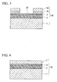
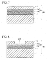
- 1 substrate, 2: multilayer reflection film, 3: protection film, 4: shock absorbing film, 4a: shock absorbing film in exposed region, 4b: shock absorbing film pattern, 44: surface of shock absorbing film in exposed region, 5: absorber layer, 5a: absorber layer pattern, 6: resist layer, 6a: resist pattern, 31: dual-use film, 31a: dual-use film upper layer, 31b: dual-use film lower layer, 311, 312: reflection region exposed after removal of absorber layer, 33: exposed reflection region, 10, 20, 50: reflection type photomask blank, 30, 40, 60: reflection type photomask.
- FIG. 1 to FIG. 3 show an embodiment according to the present invention.
- a reflection type photomask blank 10 includes: a substrate 1; a multilayer reflection film 2 formed on the substrate 1; a protection film 3 formed on the multilayer reflection film 2; a protection film 3 formed on the multilayer reflection film 2; a shock absorbing film 4 formed on the protection film 3; and an absorber layer 5 formed on the shock absorbing film 4.
- the substrate 1 is a Si substrate, a synthetic quartz substrate, or the like.
- the multilayer reflection film 2 is one that reflects EUV light (extreme ultraviolet light), which is exposure light.
- EUV light extreme ultraviolet light
- a multilayer film with a combination of materials whose refractive indices for EUV light are significantly different is used therefor.
- the multilayer reflection film 2 is formed by laminating approximately 40 cycles of layers with a combination such as Mo and Si, or Mo and Be.
- the absorber layer 5 is one which absorbs irradiated EUV light when it is dry-etched to be formed into a predetermined exposure transfer pattern as will be described later. Hence, it is selected from among heavy metals with high absorbance for the EUV light. For such a heavy metal, an alloy based on Ta can be favorably used. Furthermore, an amorphous sate of the absorber layer 5 is favorable for the purpose of obtaining an absorber layer surface with high smoothness, or performing an anisotropic etching on the absorber layer by dry etching. For example, in the case of Ta, if it is made into an alloy with an appropriate amount of Si (hereinafter referred to as TaSi-based absorber), it is allowed to be amorphous.
- TaSi-based absorber an alloy with an appropriate amount of Si
- the shock absorbing film 4 is formed from a material with resistance to the dry etching performed when the exposure transfer pattern of the absorber layer 5 is formed. It functions as an etching stopper for preventing damage to a lower layer when the absorber layer 5 is etched and is formed by the sputtering with a target of Ru.
- the protection film 3 protects the multilayer reflection film 2. It functions as an etching stopper for preventing damage to the multilayer reflection film 2 when the shock absorbing film 4 is etched and removed.
- the protection film 3 is formed from: a compound including Zr, Si, and at least either one of O and N (hereinafter referred to as ZrSiO and ZrSiN).
- ZrSiO and ZrSiN have a favorable resistance property under this etching environment.
- TABLE 1 shows etching selection ratios of the TaSi-based absorber to the compounds of ZrSi, ZrSiO, and ZrSiN, respectively, under a TaSi-based absorber etching atmosphere.
- the etching selection ratios of the TaSi-based absorber can be high to all the ZrSi-based compounds, that is, ZrSi, ZrSiO, and ZrSiN. They have a selectivity of over 20.
- the protection film 3 is formed by performing a sputtering with a target of a Zr-Si alloy in a mixed gas atmosphere of an inert gas such as Ar, and oxygen or nitrogen.
- the absorber layer 5 and the shock absorbing film 4 of such a reflection type photomask blank 10 is dry-etched in an etching atmosphere mainly composed of a chlorine gas as described above, to thereby fabricate a reflection type photomask 30 with an exposure transfer pattern in the absorber layer 5.
- an etching atmosphere mainly composed of a chlorine gas as described above
- a synthetic quartz four inches square and 0.25 inches thick whose surface was ground flat was used as a substrate 1.
- Mo and Si were alternately laminated on the substrate 1 for approximately 40 cycles by the DC magnetron sputtering, to thereby fabricate a multilayer reflection film 2 such that its reflectivity is maximized for the EUV light in a wavelength region of 13 to 14 nm.
- one cycle of the film made from Mo and Si had a thickness of 7 nm, in which the Mo film had a thickness of 2.8 nm and the Si film had a thickness of 4.2 nm.
- a protection film 3 was formed on the multilayer reflection film 2 by the DC magnetron sputtering. That is, a Zr-Si alloy target whose ratio of Zr to Si is 1:3 was used as a sputtering target. To this Zr-Si alloy target, 300 W DC was applied under an Ar atmosphere with a gas pressure of 0.25 Pa, to thereby deposit a film made from ZrSi with a thickness of 10 nm.
- a shock absorbing film 4 was formed on the protection film 3 by DC magnetron sputtering. That is, an Ru target to which 300 W DC was applied under an Ar atmosphere with a gas pressure of 0.25 Pa was used to deposit a film made from Ru with a thickness of 4 nm.
- an absorber layer 5 was formed on the shock absorbing film 4 by the DC magnetron sputtering.
- the absorber layer 5 was made of two layers. First, by a two-target sputtering using a Ta-Si alloy target and a Ta target in an Ar atmosphere, a film with a thickness of 75 nm was deposited. Subsequently, by a two-target sputtering using a Ta target and a Si target in a mixed gas atmosphere of Ar/O 2 /N 2 , a film with a thickness of 27 nm was deposited.
- the reflection type photomask blank 10 was obtained.
- the topmost surface of the mask blank in the absorber layer 5 had a surface roughness of 0.38 nmRms, and hence had a favorable surface smoothness.
- the absorber layer 5 had a reflectivity of 2.15% at a wavelength of 193 nm, and a reflectivity of 1.21 % at a wavelength of 257 nm. Therefore, a sufficiently low reflectivity property in the DUV light wavelength region for a test was obtained.
- a positive electron beam resist (FEP-171 manufactured by FUJIFILM Arch Co., Ltd.) was coated on the absorber layer 5 to form a resist layer 6.
- a resist pattern 6a was formed.
- the absorber layer 5 was etched by a dry etching apparatus of an ICP discharge type, to thereby obtain an absorber layer pattern 5a as shown in FIG. 2 .
- the reflectivity at a wavelength of 257 nm was 50.83%.
- the reflectivity at a wavelength of 257 nm on the absorber layer pattern 5a after delamination of the resist pattern 6a was 1.35%.
- the shock absorbing film 4a in the exposed region was removed. That is, a dry etching using a Cl 2 /O 2 mixed gas with the absorber layer pattern 5a as a mask was performed to form a shock absorbing film pattern 4b. Thereby, the reflection type photomask 30 of the present invention shown in FIG. 3 was obtained. At this time, in order to remove every trace of the shock absorbing film 4a in the exposed region in an even manner over the surface, a 30% overetching was performed. An etching amount in the underlying protection film 3 was 1 nm or less, and the selection ratio of the shock absorbing film 4 made from Ru to the protection film 3 made from ZrSi was 18.64. Therefore, the protection film 3 had sufficient resistance.
- the reflectivity at a wavelength of 257 nm was measured on a surface of a reflection region 33 where the absorber layer 5 and the shock absorbing film 4 were removed, and on the absorber pattern 5a.
- the results were 61.3% and 1.33%, respectively. That is, it was verified that the exposed reflection region 33 had a very high reflectivity and that there was no damage to the multilayer reflection film 2.
- a high contrast value of 95.8% was obtained, and the optical property at a test wavelength (257 nm) was favorable.
- the shock absorbing film 4 and the protection film 3 are provided, making it possible to prevent a decrease in reflectivity of the multilayer reflection film 2 when the absorber layer 5 is etched to form an exposure transfer pattern. Furthermore, according to the reflection type photomask 30 fabricated from the reflection type photomask blank 10, damage to the multilayer reflection film can be prevented to obtain a favorable reflectivity, enabling a pattern transfer with a favorable contrast. That is, such a reflection type photomask 30 enables a microscopic pattern transfer such as with a resolution of 70 nm or less by irradiation of the EUV light.
- FIG. 4 and FIG. 5 show a second embodiment according to the present invention.
- members in common with those of the aforementioned embodiment are denoted by the same reference symbols, and description thereof is omitted.
- a reflection type photomask blank 20 of this embodiment includes: a substrate 1; a multilayer reflection film 2; and an absorber layer 5, and further includes a single-layer dual-use film 31, which serves as the above-mentioned protection film 3 and the above-mentioned shock absorbing film 4, formed between the multilayer reflection film 2 and the absorber layer 5. That is, the dual-use film 31 protects multilayer reflection film 2 and also functions as an etching stopper for preventing damage to the multilayer reflection film 2 when the absorber layer 5 is etched.
- the dual-use film 31 is formed from: a compound including Zr, Si, and at least either one of O and N (ZrSiO, and ZrSiN) When formed from ZrSiO or ZrSiN, the dual-use film 31 is formed by performing a sputtering with a target of a Zr-Si alloy in a mixed gas atmosphere of an inert gas such as Ar, and oxygen or nitrogen.
- the absorber layer 5 of such a reflection type photomask blank 20 is dry-etched in an etching atmosphere mainly composed of a chlorine gas, to thereby fabricate a reflection type photomask 40 with an exposure transfer pattern in the absorber layer 5.
- etching atmosphere mainly composed of a chlorine gas
- a dual-use film formation step a dual-use film 31 was formed on the multilayer reflection film 2 by the DC magnetron sputtering. That is, a Zr-Si alloy target whose ratio of Zr to Si is 1:2 was used as a sputtering target.
- a dry etching on the absorber layer 5 was performed in the similar manner to Reference Example 1 to form an absorber pattern 5a. Thereby, a reflection type photomask 40 shown in FIG. 5 was obtained.
- a 20% overetching was performed for the purpose of removing every trace of the absorber layer 5 in the exposed region in an even manner over the surface.
- An etching amount in the dual-use film 31 was 2 nm or less, and the selection ratio of the absorber layer 5 made from the TaSi-based material to the dual-use film 31 made from ZrSiO is 26.50 as shown in TABLE 1.
- the dual-use film 31 had a favorable resistance under a dry etching environment on the absorber layer 5.
- the reflectivity at a wavelength of 257 nm was measured on a surface of a reflection region 311 where the absorber layer 5 was removed, and on the absorber pattern 5a.
- the results were 60.4% and 1.53%, respectively. That is, it was verified that the reflection region 311 had a very high reflectivity and that there was no damage to the multilayer reflection film 2.
- a high contrast value of 95.1% was obtained, and the optical property at a test wavelength (257 nm) was favorable.
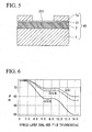
- FIG. 6 shows the result. As shown in FIG. 6 , as for the transparency for the EUV light, ZrSi has the highest value, followed by ZrSiN and ZrSiO.
- the dual-use film 31 is provided, making it possible to prevent a decrease in reflectivity when the absorber layer 5 is etched to form an exposure transfer pattern. Furthermore, the protection film and the shock absorbing film are replaced with the single-layered dual-use film 31 which serves as the protection film and the shock absorbing film, allowing the deposition process to be simplified and the film to be thinner. Furthermore, similarly to the first embodiment, the reflection type photomask 40 fabricated from the reflection type photomask blank 20 enables a pattern transfer with a favorable contrast, and also enables a microscopic pattern transfer such as with a resolution of 70 nm or less by irradiation of the EUV light.
- FIG. 7 and FIG. 8 show a third embodiment according to the present invention.
- members in common with those of the aforementioned embodiments are denoted by the same reference symbols, and description thereof is omitted.
- a reflection type photomask blank 50 of this embodiment includes: a substrate 1; a multilayer reflection film 2; and an absorber layer 5, and further includes a dual-use film 31, which serves as a protection film 3 and a shock absorbing film 4, formed between the multilayer reflection film 2 and the absorber layer 5.
- the dual-use film 31 has a laminated configuration of a plurality of dual-use films. In the present embodiment, it is made of two layers of: a dual-use film upper layer 31a and a dual-use film lower layer 31b.
- the dual-use film 31 is allowed to have a more favorable etching resistance while suppressing a decrease in reflectivity of the mask for the EUV light.
- the dual-use film 31 is formed from a dual-use film upper layer 31a and a dual-use film lower layer 31b are ZrSiO and ZrSi; ZrSiN and ZrSi; and C and ZrSi, respectively.
- the dual-use film 31 is not limited to two layers of the dual-use film upper layer 31a and the dual-use film lower layer 31b, but may be formed of further more layers.
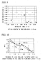
- FIG. 9 shows optical constants (refractive index and extinction coefficient) of the respective material for the EUV light.
- TABLE 2 below shows ratios of the etching rates of ZrSi, ZrSiN, ZrSiO, Ru, and C to the etching rate of the EUV light absorption film made from TaSi. If a material with high transmittance for the EUV light is selected for the dual-use film lower layer 31b, and a material with high etching resistance is selected for the dual-use film upper layer 31a with reference to the above figure and table, it is possible to increase a degree of freedom of etching while suppressing a decrease in reflectivity of the EUV light.
- the reflection type photomask blank 50 of the present embodiment and a manufacturing method thereof and a description of the reflection type photomask 60, based on Example 4 to Example 9.
- the details of a substrate 1 and a multilayer reflection film 2, and a multilayer reflection film formation step, which is a manufacturing step thereof, are omitted because they are similar to those of Example 1.
- a dual-use film upper layer 31 a and a dual-use film lower layer 31b were formed on a multilayer reflection film 2.
- the dual-use film upper layer 31a was a ZrSiO film.
- ZrSiO has a high resistance to etching.
- the dual-use film lower layer 31b was a ZrSi film.
- both Zr and Si have a high transparency for the EUV wavelength.
- the dual-use film upper layer 31a and the dual-use film lower layer 31b were fabricated by the DC magnetron sputtering respectively under the following conditions.
- a Zr-Si alloy target whose ratio of Zr to Si is 1:3 was used as a sputtering target.
- 300 W DC was applied under an Ar atmosphere with a gas pressure of 0.25 Pa, to thereby deposit a film with a thickness of 5 nm.
- a ZrSi 2 target was used as a sputtering target.
- 300 W DC was applied under an Ar atmosphere with a gas pressure of 0.25 Pa to which was added O 2 to deposit a film with a thickness of 5 nm.
- an absorber layer 5 was formed, to thereby obtain a reflection type photomask blank 50.
- the topmost surface of the reflection type photomask blank 50 in the absorber layer 5 had a surface roughness of 0.38 nmRms, and hence had a favorable surface smoothness.
- the results of the measurement of the reflectivity on the surface of the absorber layer 5 were 2.15% at a wavelength of 193 nm and 1.21% at a wavelength of 257 nm. Therefore, a sufficiently low reflectivity property in the DUV light wavelength region for a test was obtained.
- the reflectivity of a test wavelength at 257 nm on the reflection region 312 which was exposed after partial removal of the absorber layer 5 was 50.11%.
- the reflectivity at 257 nm on the surface of the absorber pattern 5a of the photomask 60 of FIG. 8 after delamination of the resist pattern 6a was 1.35%.
- a favorable contrast value of 94.7% was obtained, and the optical property at a test wavelength (257 nm) was favorable.
- FIG. 10 is a simulation results of the reflectivity for the EUV wavelength on the reflection region 312 which is exposed after partial removal of the absorber layer 5 by etching, in the case where the dual-use film 31 of the present invention has a laminated configuration of the dual-use film lower layer 31b and the dual-use film upper layer 31a.
- a result has been shown that by making the thickness of the ZrSiO film as the dual-use film upper layer 31a 4.0 nm or less when the ZrSi film as the dual-use film lower layer 31b has a thickness of 5.0 nm, it is theoretically possible to obtain a reflectivity over 67.5% for the EUV light.
- a dual-use film upper layer 31a and a dual-use film lower layer 31b were formed on a multilayer reflection film 2.
- the dual-use film upper layer 31 a was a ZrSiN film.
- ZrSiN has a high resistance to etching.
- the dual-use film lower layer 31b was a ZrSi film.
- both Zr and Si have a high transparency for the EUV wavelength.
- the dual-use film upper layer 31a and the dual-use film lower layer 31b were fabricated by the DC magnetron sputtering respectively under the following conditions.
- a Zr-Si alloy target whose ratio of Zr to Si is 1:3 was used as a sputtering target.
- 300 W DC was applied under an Ar atmosphere with a gas pressure of 0.25 Pa, to thereby deposit a film with a thickness of 5 nm.
- a ZrSi 2 target was used as a sputtering target.
- 300 W DC was applied under an Ar atmosphere with a gas pressure of 0.25 Pa to which was added N 2 , to thereby deposit a film with a thickness of 5 nm.
- an absorber layer 5 was formed, to thereby obtain a reflection type photomask blank 50.
- the topmost surface of the reflection type photomask blank 50 in the absorber layer 5 had a surface roughness of 0.40 nmRms, and hence had a favorable surface smoothness.
- the results of the measurement of the reflectivity on the surface of the absorber layer 5 were 2.18% at a wavelength of 193 nm and 1.25% at a wavelength of 257 nm. Therefore, a sufficiently low reflectivity property in the DUV light wavelength region for a test was obtained.
- the reflectivity of a test wavelength at 257 nm on the reflection region 312 which was exposed after partial removal of the absorber layer 5 was 51.47%.
- the reflectivity at 257 nm on the surface of the absorber pattern 5a of the photomask 60 of FIG. 8 after delamination of the resist pattern 6a was 1.38%.
- a favorable contrast value of 94.7% was obtained, and the optical property at a test wavelength (257 nm) was favorable.
- a dual-use film upper layer 31a and a dual-use film lower layer 31b were formed on a multilayer reflection film 2.
- the dual-use film upper layer 31a was a Ru film.
- Ru has a high resistance to etching.
- the dual-use film lower layer 31b was a ZrSi film. As shown in FIG. 9 , both Zr and Si have a high transparency for the EUV wavelength.
- the dual-use film upper layer 31a and the dual-use film lower layer 31b were fabricated by the DC magnetron sputtering respectively under the following conditions.
- a Zr-Si alloy target whose ratio of Zr to Si is 1:3 was used as a sputtering target.
- 300 W DC was applied under an Ar atmosphere with a gas pressure of 0.25 Pa, to thereby deposit a film with a thickness of 5 nm.
- a Ru target was used as a sputtering target.
- 300 W DC was applied under an Ar atmosphere with a gas pressure of 0.25 Pa, to thereby deposit a film with a thickness of 2 nm.
- an absorber layer 5 was formed, to thereby obtain a reflection type photomask blank 50.
- the topmost surface of the reflection type photomask blank 50 in the absorber layer 5 had a surface roughness of 0.37 nmRms, and hence had a favorable surface smoothness.
- the results of the measurement of the reflectivity on the surface of the absorber layer 5 were 2.22% at a wavelength of 193 nm and 1.24% at a wavelength of 257 nm. Therefore, a sufficiently low reflectivity property in the DUV light wavelength region for a test was obtained.
- the reflectivity of a test wavelength at 257 nm on the reflection region 312 which was exposed after partial removal of the absorber layer 5 was 50.33%.
- the reflectivity at 257 nm on the surface of the absorber pattern 5a of the photomask 60 of FIG. 8 after delamination of the resist pattern 6a was 1.33%.
- a favorable contrast value of 94.8% was obtained, and the optical property at a test wavelength (257 nm) was favorable.
- a dual-use film upper layer 31a and a dual-use film lower layer 31b were formed on a multilayer reflection film 2.
- the dual-use film upper layer 31a was a C film. As shown in TABLE 2, C has a high resistance to etching.
- the dual-use film lower layer 31b was a ZrSi film. As shown in FIG. 9 , both Zr and Si have a high transparency for the EUV wavelength.
- the dual-use film upper layer 31a and the dual-use film lower layer 31b were fabricated under the following conditions.
- a Zr-Si alloy target whose ratio of Zr to Si is 1:3 was used as a sputtering target.
- 300 W DC was applied under an Ar atmosphere with a gas pressure of 0.25 Pa, to thereby deposit a film with a thickness of 5 nm.
- a parallel-plate plasma CVD apparatus was used to form a dual-use film upper layer 31a, which was a diamond-shaped carbon thin film, on the dual-use film lower layer 31b.
- the conditions for the plasma CVD were that a gas whose major component was methane (flow rate: 20 sccm) was used as a material gas, and that a gas including nitrogen (concentration: 1 to 50%) was used as a doping gas.
- a reaction pressure was set to 0.03 Torr, and a self-bias voltage was set to 0 to 1500 V.
- the dual-use film upper layer 31a with a thickness of 5 nm was deposited.
- an absorber layer 5 was formed, to thereby obtain a reflection type photomask blank 50.
- the topmost surface of the reflection type photomask blank 50 in the absorber layer 5 had a surface roughness of 0.39 nmRms, and hence had a favorable surface smoothness.
- the results of the measurement of the reflectivity on the surface of the absorber layer 5 were 2.15% at a wavelength of 193 nm and 1.21% at a wavelength of 257 nm. Therefore, sufficiently low reflectivity property in the DUV light wavelength region for a test was obtained.
- the reflectivity of a test wavelength at 257 nm on the reflection region 312 which was exposed after partial removal of the absorber layer 5 was 50.01%.
- the reflectivity at 257 nm on the surface of the absorber pattern 5a of the photomask 60 of FIG. 8 after delamination of the resist pattern 6a was 1.53%.
- a favorable contrast value of 94.1% was obtained, and the optical property at a test wavelength (257 nm) was favorable.
- a dual-use film upper layer 31a and a dual-use film lower layer 31b were formed on a multilayer reflection film 2.
- the dual-use film upper layer 31 a was a Ru film.
- Ru has a high resistance to etching.
- the dual-use film lower layer 31b was a C film. As shown in FIG. 9 , C has a high transparency for the EUV wavelength.
- the dual-use film upper layer 31a and the dual-use film lower layer 31b were fabricated respectively under the following conditions.
- a parallel-plate plasma CVD apparatus was used to form a dual-use film lower layer 31b which was a diamond-shaped carbon thin film.
- the conditions for the plasma CVD were that a gas whose major component was methane (flow rate: 20 sccm) was used as a material gas, and that a gas including nitrogen (concentration: 1 to 50%) was used as a doping gas.
- a reaction pressure was set to 0.03 Torr, and a self-bias voltage was set to 0 to 1500 V.
- the dual-use film lower layer 31b with a thickness of 5 nm was deposited.
- a Ru target was used as a sputtering target.
- 300 W DC was applied under an Ar atmosphere with a gas pressure of 0.25 Pa, to thereby deposit a film with a thickness of 2 nm.
- an absorber layer 5 was formed, to thereby obtain a reflection type photomask blank 50.
- the topmost surface of the reflection type photomask blank 50 in the absorber layer 5 had a surface roughness of 0.41 nmRms, and hence had a favorable surface smoothness.
- the results of the measurement of the reflectivity on the surface of the absorber layer 5 were 2.22% at a wavelength of 193 nm and 1.24% at a wavelength of 257 nm. Therefore, a sufficiently low reflectivity property in the DUV light wavelength region for a test was obtained.
- the reflectivity of a test wavelength at 257 nm on the reflection region 312 which was a region exposed after partial removal of the absorber layer 5 was 49.89%.
- the reflectivity at 257 nm on the surface of the absorber pattern 5a of the photomask 60 of FIG. 8 after delamination of the resist pattern 6a was 1.33%.
- a favorable contrast value of 94.8% was obtained, and the optical property at a test wavelength (257 nm) was favorable.
- the dual-use film 31 has a laminated configuration of a plurality of layers, making it possible to prevent a decrease in reflectivity when the absorber layer 5 is etched to form an exposure transfer pattern. Furthermore, the laminated configuration allows the dual-use film 31 to sufficiently have both of etching resistance and transmittance for the EUV light. Furthermore, similarly to the first embodiment, the reflection type photomask 60 fabricated from the reflection type photomask blank 50 enables a pattern transfer with a favorable contrast, and also enables a microscopic pattern transfer such as with a resolution of 70 nm or less by irradiation of the EUV light.
- a microscopic pattern with a resolution of 70 nm or less can be transferred to manufacture a semiconductor device. That is, as a transfer step, the EUV light as exposure light is irradiated onto the reflection type photomask 30 (40, 60). The reflected light reflected on the multilayer reflection film 2 of the reflection type photomask 30 (40, 60) exposes a resist layer provided on a semiconductor substrate, allowing a range corresponding to the wavelength of the irradiated EUV light, that is, a microscopic pattern with a resolution of 70 nm or less to be transferred with a favorable contrast. Therefore, in the manufacturing method of a semiconductor device with such a transfer step, it is possible to manufacture a semiconductor device subjected to micromachining at 70 nm or less which corresponds to the wavelength of the EUV light as exposure light.
- the reflection type photomask blank of the present invention is applicable for preventing a decrease in reflectivity when an absorber layer is etched to from an exposure transfer pattern. Furthermore, the reflection type photomask of the present invention is applicable for preventing damage to a multilayer reflection film to obtain a favorable reflectivity, enabling a pattern transfer with a favorable contrast.
Landscapes
- Engineering & Computer Science (AREA)
- Physics & Mathematics (AREA)
- Nanotechnology (AREA)
- Chemical & Material Sciences (AREA)
- General Physics & Mathematics (AREA)
- Crystallography & Structural Chemistry (AREA)
- Condensed Matter Physics & Semiconductors (AREA)
- Theoretical Computer Science (AREA)
- Mathematical Physics (AREA)
- Manufacturing & Machinery (AREA)
- Spectroscopy & Molecular Physics (AREA)
- General Engineering & Computer Science (AREA)
- High Energy & Nuclear Physics (AREA)
- Preparing Plates And Mask In Photomechanical Process (AREA)
- Exposure Of Semiconductors, Excluding Electron Or Ion Beam Exposure (AREA)
- Exposure And Positioning Against Photoresist Photosensitive Materials (AREA)
Claims (10)
- Ebauche de photomasque du type à réflexion pour lithographie aux ultraviolets extrêmes, comprenant :un substrat (1) ;un film de réflexion multicouche (2) formé sur le substrat (1) pour réfléchir une lumière d'exposition ;un film de protection (3) formé sur le film de réflexion multicouche (2) pour le protéger ;une couche d'absorption (5) pour absorber la lumière d'exposition sur les films de protection (3) ; etun film amortisseur de chocs (4) composé de Ru formé entre la couche d'absorption (5) et le film de protection (3), ayant une résistance à la gravure qui est effectuée lorsqu'un motif de transfert d'exposition de la couche d'absorption (5) est formé, oùle film de protection (3) est : ZrSiO ou ZrSiN.
- Ebauche de photomasque du type à réflexion pour lithographie aux ultraviolets extrêmes, comprenant :un substrat (1) ;un film de réflexion multicouche (2) formé sur le substrat (1) pour réfléchir la lumière d'exposition ;une couche d'absorption (5) formée sur le film de réflexion multicouche (2) pour absorber la lumière d'exposition ; etun film monocouche à double usage (31) formé entre le film de réflexion multicouche (2) et la couche d'absorption (5) pour protéger le film de réflexion multicouche (2), ayant une résistance à la gravure qui est effectuée lorsqu'un motif de transfert d'exposition de la couche d'absorption (5) est formé, oùle film à double usage (31) est : ZrSiO ou ZrSiN.
- Ebauche de photomasque du type à réflexion pour lithographie aux ultraviolets extrêmes, comprenant :un substrat (1) ;un film de réflexion multicouche (2) formé sur le substrat (1) pour réfléchir la lumière d'exposition ;une couche d'absorption (5) formée sur le film de réflexion multicouche (2) pour absorber la lumière d'exposition ; etune pluralité de films à double usage comprenant une couche inférieure (31b) de film à double usage et une couche supérieure (31a) de film à double usage formées entre le film de réflexion multicouche (2) et la couche d'absorption (5) pour protéger le film de réflexion multicouche (2), ayant une résistance à la gravure qui est effectuée lorsqu'un motif de transfert d'exposition de la couche d'absorption (5) est formé, où ladite couche supérieure (31a) et ladite couche inférieure (31b) sont ZrSiO et ZrSi ; ZrSiN et ZrSi ; et C et ZrSi, respectivement.
- Procédé de fabrication d'une ébauche de photomasque du type à réflexion selon la revendication 1, comprenant :une étape de formation d'un film de réflexion multicouche qui consiste à former le film de réflexion multicouche (2) sur le substrat (1) ;une étape de formation d'un film de protection qui consiste à former un film de protection (3) sur le film de réflexion multicouche (2) en effectuant une pulvérisation avec une cible de Zr-Si dans une atmosphère de gaz mixte comportant un gaz inerte et au moins l'un parmi l'oxygène et l'azote,une étape de formation d'un film amortisseur de chocs qui consiste à former un film amortisseur de chocs (4) sur le film de protection en effectuant une pulvérisation avec une cible de Ru ; etune étape de formation d'une couche d'absorption qui consiste à former la couche d'absorption (5) sur le film amortisseur de chocs (4).
- Procédé de fabrication d'une ébauche de photomasque du type à réflexion selon la revendication 2, comprenant :une étape de formation d'un film de réflexion multicouche qui consiste à former le film de réflexion multicouche (2) sur le substrat (1) ;une étape de formation d'un film à double usage qui consiste à former un film à double usage (31) sur le film de réflexion multicouche (2) en effectuant une pulvérisation avec une cible d'alliage Zr-Si dans une atmosphère de gaz mixte comportant un gaz inerte et au moins l'un parmi l'oxygène et l'azote ; etune étape de formation d'un couche d'absorption qui consiste à former la couche d'absorption (5) sur le film à double usage (31).
- Procédé de fabrication d'une ébauche de photomasque du type à réflexion selon la revendication 3, comprenant :une étape de formation d'un film de réflexion multicouche qui consiste à former le film de réflexion multicouche (2) sur le substrat (1) ;une étape de formation d'un film à double usage qui consiste à former un film à double usage (31) sur le film de réflexion multicouche (2) en effectuant une pulvérisation avec une cible d'un alliage Zr-Si dans une atmosphère de gaz inerte ou dans une atmosphère de gaz mixte comportant un gaz inerte et au moins l'un parmi l'oxygène et l'azote, ou en effectuant un Dépôt Chimique en Phase Vapeur avec un composé comportant du C en tant que gaz de matériau ; etune étape de formation d'une couche d'absorption qui consiste à former la couche d'absorption (5) sur le film à double usage (31), oùl'étape de formation d'un film à double usage comporte le fait de stratifier une pluralité de films à double usage sur le film de réflexion multicouche (2).
- Photomasque du type à réflexion, dans lequel un motif de transfert d'exposition est formé par gravure d'une couche d'absorption (5) de l'ébauche de photomasque du type à réflexion selon l'une quelconque des revendications 1 à 3.
- Photomasque du type à réflexion selon la revendication 7, dans lequel le motif de transfert d'exposition est formé par gravure de la couche d'absorption (5) et du film amortisseur de chocs (4) d'une ébauche de photomasque du type à réflexion selon la revendication 1.
- Photomasque du type à réflexion selon la revendication 7, dans lequel le motif de transfert d'exposition est formé en gravant uniquement la couche d'absorption (5) de l'ébauche de photomasque du type à réflexion selon la revendication 2 ou 3.
- Procédé de fabrication d'un dispositif à semi-conducteur, comprenant une étape de transfert qui consiste à transférer le motif de la couche d'absorption (5) du photomasque du type à réflexion sur une couche de réserve prévue sur un substrat semi-conducteur en irradiant de la lumière ultraviolette extrême comme étant la lumière d'exposition sur le photomasque du type à réflexion selon l'une des revendications 5 à 9 afin d'exposer la lumière réfléchie sur le film de réflexion multicouche du photomasque du type à réflexion sur la couche de réserve.
Applications Claiming Priority (3)
| Application Number | Priority Date | Filing Date | Title |
|---|---|---|---|
| JP2006093304 | 2006-03-30 | ||
| JP2006251160A JP4946296B2 (ja) | 2006-03-30 | 2006-09-15 | 反射型フォトマスクブランク及びその製造方法、反射型フォトマスク、並びに、半導体装置の製造方法 |
| PCT/JP2006/324368 WO2007116562A1 (fr) | 2006-03-30 | 2006-12-06 | Decoupe de masque photographique reflechissant, procede de production de celle-ci, masque photographique reflechissant et procede de production d'un dispositif a semi-conducteurs |
Publications (3)
| Publication Number | Publication Date |
|---|---|
| EP2015139A1 EP2015139A1 (fr) | 2009-01-14 |
| EP2015139A4 EP2015139A4 (fr) | 2009-04-22 |
| EP2015139B1 true EP2015139B1 (fr) | 2013-05-01 |
Family
ID=38580864
Family Applications (1)
| Application Number | Title | Priority Date | Filing Date |
|---|---|---|---|
| EP06834123.9A Active EP2015139B1 (fr) | 2006-03-30 | 2006-12-06 | Decoupe de masque photographique reflechissant, procede de production de celle-ci, masque photographique reflechissant et procede de production d'un dispositif a semi-conducteurs |
Country Status (6)
| Country | Link |
|---|---|
| US (1) | US8394558B2 (fr) |
| EP (1) | EP2015139B1 (fr) |
| JP (1) | JP4946296B2 (fr) |
| KR (1) | KR20080104267A (fr) |
| TW (1) | TWI441238B (fr) |
| WO (1) | WO2007116562A1 (fr) |
Families Citing this family (12)
| Publication number | Priority date | Publication date | Assignee | Title |
|---|---|---|---|---|
| JP5638769B2 (ja) * | 2009-02-04 | 2014-12-10 | Hoya株式会社 | 反射型マスクブランクの製造方法及び反射型マスクの製造方法 |
| KR101054746B1 (ko) * | 2009-07-22 | 2011-08-05 | 한양대학교 산학협력단 | 극자외선 노광 공정용 위상 반전 마스크 |
| TWI464529B (zh) | 2009-12-09 | 2014-12-11 | 旭硝子股份有限公司 | EUV microfilm with anti-reflective substrate, EUV microsurgical reflective mask substrate, EUV microsurgical reflective mask and manufacturing method of the reflective substrate |
| KR20130111524A (ko) * | 2010-07-27 | 2013-10-10 | 아사히 가라스 가부시키가이샤 | Euv 리소그래피용 반사층 형성 기판, 및 euv 리소그래피용 반사형 마스크 블랭크 |
| JP5772135B2 (ja) * | 2011-03-28 | 2015-09-02 | 凸版印刷株式会社 | 反射型マスクブランク及び反射型マスク |
| CN102809896B (zh) * | 2011-05-30 | 2014-03-19 | 中芯国际集成电路制造(上海)有限公司 | 掩膜版及其光刻方法 |
| WO2013141268A1 (fr) * | 2012-03-23 | 2013-09-26 | Hoya株式会社 | Substrat avec film réfléchissant multicouche, ébauche de masque réfléchissant pour la lithographie euv, procédé de production d'une ébauche réfléchissante pour la lithographie euv, et procédé de fabrication d'un dispositif à semi-conducteur |
| JP2014127630A (ja) * | 2012-12-27 | 2014-07-07 | Asahi Glass Co Ltd | Euvリソグラフィ用反射型マスクブランクおよびその製造方法 |
| KR102171266B1 (ko) * | 2013-08-01 | 2020-10-28 | 삼성전자 주식회사 | 반사형 포토마스크 블랭크 및 반사형 포토마스크와 포토마스크를 이용하여 제조된 집적회로 소자 |
| WO2018226370A1 (fr) * | 2017-06-08 | 2018-12-13 | Applied Materials, Inc. | Films de carbone à basse température haute densité pour masque dur et autres applications de formation de motifs |
| NL2027098B1 (en) * | 2020-01-16 | 2021-10-14 | Asml Netherlands Bv | Pellicle membrane for a lithographic apparatus |
| US20240231214A9 (en) * | 2021-03-02 | 2024-07-11 | Hoya Corporation | Substrate with multilayer reflective film, reflective mask blank, reflective mask, and method for manufacturing semiconductor device |
Citations (1)
| Publication number | Priority date | Publication date | Assignee | Title |
|---|---|---|---|---|
| US20030198874A1 (en) * | 2002-04-18 | 2003-10-23 | Lee Byoung-Taek | Reflection photomasks with a capping layer and methods for manufacturing the same |
Family Cites Families (20)
| Publication number | Priority date | Publication date | Assignee | Title |
|---|---|---|---|---|
| JP3266994B2 (ja) * | 1993-07-28 | 2002-03-18 | 株式会社ニコン | 反射型マスク |
| US6013399A (en) * | 1998-12-04 | 2000-01-11 | Advanced Micro Devices, Inc. | Reworkable EUV mask materials |
| TWI267704B (en) | 1999-07-02 | 2006-12-01 | Asml Netherlands Bv | Capping layer for EUV optical elements |
| US6596465B1 (en) | 1999-10-08 | 2003-07-22 | Motorola, Inc. | Method of manufacturing a semiconductor component |
| JP4397496B2 (ja) | 2000-02-25 | 2010-01-13 | Okiセミコンダクタ株式会社 | 反射型露光マスクおよびeuv露光装置 |
| JP5371162B2 (ja) * | 2000-10-13 | 2013-12-18 | 三星電子株式会社 | 反射型フォトマスク |
| EP1260862B1 (fr) | 2001-05-21 | 2012-04-11 | ASML Netherlands B.V. | Appareil lithographique, méthodes pour fabriquer des éléments, méthode pour fabriquer un réflecteur ainsi qu'un masque à décalage de phase |
| US6818357B2 (en) | 2001-10-03 | 2004-11-16 | Intel Corporation | Photolithographic mask fabrication |
| DE10150874A1 (de) * | 2001-10-04 | 2003-04-30 | Zeiss Carl | Optisches Element und Verfahren zu dessen Herstellung sowie ein Lithographiegerät und ein Verfahren zur Herstellung eines Halbleiterbauelements |
| EP1333323A3 (fr) | 2002-02-01 | 2004-10-06 | Nikon Corporation | Elément optique autonettoyant pour un système optique à rayons X, ainsi que des systèmes optiques et microlithographiques contenant cet élément |
| EP2317383A3 (fr) | 2002-04-11 | 2011-12-28 | HOYA Corporation | Ébauche de masque réfléchissant, masque réfléchissant et procédés de fabrication de l'ébauche de masque et masque |
| JP4212025B2 (ja) * | 2002-07-04 | 2009-01-21 | Hoya株式会社 | 反射型マスクブランクス及び反射型マスク並びに反射型マスクの製造方法 |
| JP4521753B2 (ja) | 2003-03-19 | 2010-08-11 | Hoya株式会社 | 反射型マスクの製造方法及び半導体装置の製造方法 |
| JP4521696B2 (ja) * | 2003-05-12 | 2010-08-11 | Hoya株式会社 | 反射多層膜付き基板及び反射型マスクブランクス並びに反射型マスク |
| JP2004342734A (ja) * | 2003-05-14 | 2004-12-02 | Hoya Corp | 反射型マスクブランクス及び反射型マスク |
| FR2865813B1 (fr) * | 2004-01-30 | 2006-06-23 | Production Et De Rech S Appliq | Masque a motifs proteges, pour la lithographie par reflexion dans le domaine de l'extreme uv et des rayons x mous |
| US7282307B2 (en) * | 2004-06-18 | 2007-10-16 | Freescale Semiconductor, Inc. | Reflective mask useful for transferring a pattern using extreme ultra violet (EUV) radiation and method of making the same |
| JP4553239B2 (ja) * | 2004-06-29 | 2010-09-29 | Hoya株式会社 | 反射型マスクブランクス及び反射型マスク並びに半導体装置の製造方法 |
| JP5256569B2 (ja) * | 2005-02-15 | 2013-08-07 | 凸版印刷株式会社 | 極端紫外線露光用マスク、マスクブランク、露光方法及びマスクブランクの製造方法 |
| JP2006332153A (ja) * | 2005-05-24 | 2006-12-07 | Hoya Corp | 反射型マスクブランク及び反射型マスク並びに半導体装置の製造方法 |
-
2006
- 2006-09-15 JP JP2006251160A patent/JP4946296B2/ja not_active Expired - Fee Related
- 2006-12-06 EP EP06834123.9A patent/EP2015139B1/fr active Active
- 2006-12-06 WO PCT/JP2006/324368 patent/WO2007116562A1/fr not_active Ceased
- 2006-12-06 KR KR1020087018832A patent/KR20080104267A/ko not_active Withdrawn
-
2007
- 2007-01-17 TW TW096101666A patent/TWI441238B/zh not_active IP Right Cessation
-
2008
- 2008-09-23 US US12/232,757 patent/US8394558B2/en active Active
Patent Citations (1)
| Publication number | Priority date | Publication date | Assignee | Title |
|---|---|---|---|---|
| US20030198874A1 (en) * | 2002-04-18 | 2003-10-23 | Lee Byoung-Taek | Reflection photomasks with a capping layer and methods for manufacturing the same |
Also Published As
| Publication number | Publication date |
|---|---|
| JP2007294840A (ja) | 2007-11-08 |
| TW200737300A (en) | 2007-10-01 |
| EP2015139A4 (fr) | 2009-04-22 |
| US20090042110A1 (en) | 2009-02-12 |
| EP2015139A1 (fr) | 2009-01-14 |
| KR20080104267A (ko) | 2008-12-02 |
| JP4946296B2 (ja) | 2012-06-06 |
| US8394558B2 (en) | 2013-03-12 |
| WO2007116562A1 (fr) | 2007-10-18 |
| TWI441238B (zh) | 2014-06-11 |
Similar Documents
| Publication | Publication Date | Title |
|---|---|---|
| US8394558B2 (en) | Reflection type photomask blank, manufacturing method thereof, reflection type photomask, and manufacturing method of semiconductor device | |
| JP7502510B2 (ja) | 反射型マスクブランク、反射型マスク、及び半導体装置の製造方法 | |
| US10481484B2 (en) | Reflective mask blank, reflective mask, method for manufacturing reflective mask blank, and method for manufacturing semiconductor device | |
| JP5194888B2 (ja) | 反射型フォトマスクブランク及びその製造方法、反射型フォトマスク及びその製造方法並びに半導体素子の製造方法 | |
| JP4525893B2 (ja) | 位相シフトマスクブランク、位相シフトマスク及びパターン転写方法 | |
| KR100906026B1 (ko) | 반사형 포토마스크 블랭크, 반사형 포토마스크, 및 이것을이용한 반도체 장치의 제조 방법 | |
| WO2009136564A1 (fr) | Masque réfléchissant, ébauche de masque réfléchissant et procédé de fabrication d'un masque réfléchissant | |
| KR20160034315A (ko) | 다층 반사막을 구비한 기판, euv 리소그래피용 반사형 마스크 블랭크, euv 리소그래피용 반사형 마스크 및 그 제조 방법과 반도체 장치의 제조 방법 | |
| US11360377B2 (en) | Half-tone attenuated phase shift blankmask and photomask for EUV lithography | |
| JP5292747B2 (ja) | 極端紫外線用反射型フォトマスク | |
| JP2021184108A (ja) | 多層反射膜付き基板、反射型マスクブランク、反射型マスク、及び半導体デバイスの製造方法 | |
| KR102541867B1 (ko) | 표시 장치 제조용 위상 시프트 마스크 블랭크, 표시 장치 제조용 위상 시프트 마스크의 제조 방법 및 표시 장치의 제조 방법 | |
| JP2006228766A (ja) | 極端紫外線露光用マスク、マスクブランク、及び露光方法 | |
| JP4998082B2 (ja) | 反射型フォトマスクブランク及びその製造方法、反射型フォトマスク、並びに、半導体装置の製造方法 | |
| KR20160016098A (ko) | 극자외선용 블랭크 마스크 및 이를 이용한 포토마스크 | |
| JP2005284213A (ja) | 位相シフトマスクブランク、位相シフトマスク及びパターン転写方法 | |
| TW202201110A (zh) | 極紫外光微影相移光罩 | |
| JP4320050B2 (ja) | 反射型マスクブランクス及びその製造方法、反射型マスク | |
| US20070275308A1 (en) | Reflective mask blank, reflective mask, and method of manufacturing semiconductor device | |
| KR102109865B1 (ko) | 블랭크 마스크, 위상반전 포토마스크 및 그의 제조 방법 | |
| TW202331406A (zh) | 反射型光罩基底、反射型光罩、反射型光罩之製造方法 | |
| JP2022135928A (ja) | 反射型マスクブランク及びその製造方法 | |
| KR20230031473A (ko) | 크롬 및 니오븀을 함유한 하드마스크막을 구비한 극자외선 리소그래피용 블랭크마스크 및 포토마스크 | |
| JP2007207829A (ja) | 反射型マスクブランク、反射型フォトマスク、及び反射型フォトマスクの製造方法 | |
| JP4300930B2 (ja) | 極限紫外線露光用マスク及びブランク並びにパターン転写方法 |
Legal Events
| Date | Code | Title | Description |
|---|---|---|---|
| PUAI | Public reference made under article 153(3) epc to a published international application that has entered the european phase |
Free format text: ORIGINAL CODE: 0009012 |
|
| 17P | Request for examination filed |
Effective date: 20080925 |
|
| AK | Designated contracting states |
Kind code of ref document: A1 Designated state(s): AT BE BG CH CY CZ DE DK EE ES FI FR GB GR HU IE IS IT LI LT LU LV MC NL PL PT RO SE SI SK TR |
|
| AX | Request for extension of the european patent |
Extension state: AL BA HR MK RS |
|
| A4 | Supplementary search report drawn up and despatched |
Effective date: 20090323 |
|
| 17Q | First examination report despatched |
Effective date: 20090730 |
|
| R17C | First examination report despatched (corrected) |
Effective date: 20100126 |
|
| REG | Reference to a national code |
Ref country code: DE Ref legal event code: R079 Ref document number: 602006036106 Country of ref document: DE Free format text: PREVIOUS MAIN CLASS: G03F0001160000 Ipc: G03F0001240000 |
|
| RIC1 | Information provided on ipc code assigned before grant |
Ipc: G21K 1/06 20060101ALI20120410BHEP Ipc: G03F 1/48 20120101ALI20120410BHEP Ipc: G03F 1/24 20120101AFI20120410BHEP |
|
| GRAP | Despatch of communication of intention to grant a patent |
Free format text: ORIGINAL CODE: EPIDOSNIGR1 |
|
| GRAS | Grant fee paid |
Free format text: ORIGINAL CODE: EPIDOSNIGR3 |
|
| GRAA | (expected) grant |
Free format text: ORIGINAL CODE: 0009210 |
|
| RAP1 | Party data changed (applicant data changed or rights of an application transferred) |
Owner name: TOPPAN PRINTING CO., LTD. |
|
| RIN1 | Information on inventor provided before grant (corrected) |
Inventor name: MATSUO, TADASHI Inventor name: TAMURA, SHINPEI Inventor name: KANAYAMA, KOICHIRO |
|
| AK | Designated contracting states |
Kind code of ref document: B1 Designated state(s): AT BE BG CH CY CZ DE DK EE ES FI FR GB GR HU IE IS IT LI LT LU LV MC NL PL PT RO SE SI SK TR |
|
| AX | Request for extension of the european patent |
Extension state: AL BA HR MK RS |
|
| REG | Reference to a national code |
Ref country code: GB Ref legal event code: FG4D |
|
| REG | Reference to a national code |
Ref country code: CH Ref legal event code: EP Ref country code: AT Ref legal event code: REF Ref document number: 610278 Country of ref document: AT Kind code of ref document: T Effective date: 20130515 |
|
| REG | Reference to a national code |
Ref country code: IE Ref legal event code: FG4D |
|
| REG | Reference to a national code |
Ref country code: DE Ref legal event code: R096 Ref document number: 602006036106 Country of ref document: DE Effective date: 20130627 |
|
| REG | Reference to a national code |
Ref country code: AT Ref legal event code: MK05 Ref document number: 610278 Country of ref document: AT Kind code of ref document: T Effective date: 20130501 |
|
| REG | Reference to a national code |
Ref country code: NL Ref legal event code: VDEP Effective date: 20130501 |
|
| REG | Reference to a national code |
Ref country code: LT Ref legal event code: MG4D |
|
| PG25 | Lapsed in a contracting state [announced via postgrant information from national office to epo] |
Ref country code: GR Free format text: LAPSE BECAUSE OF FAILURE TO SUBMIT A TRANSLATION OF THE DESCRIPTION OR TO PAY THE FEE WITHIN THE PRESCRIBED TIME-LIMIT Effective date: 20130802 Ref country code: SI Free format text: LAPSE BECAUSE OF FAILURE TO SUBMIT A TRANSLATION OF THE DESCRIPTION OR TO PAY THE FEE WITHIN THE PRESCRIBED TIME-LIMIT Effective date: 20130501 Ref country code: AT Free format text: LAPSE BECAUSE OF FAILURE TO SUBMIT A TRANSLATION OF THE DESCRIPTION OR TO PAY THE FEE WITHIN THE PRESCRIBED TIME-LIMIT Effective date: 20130501 Ref country code: FI Free format text: LAPSE BECAUSE OF FAILURE TO SUBMIT A TRANSLATION OF THE DESCRIPTION OR TO PAY THE FEE WITHIN THE PRESCRIBED TIME-LIMIT Effective date: 20130501 Ref country code: ES Free format text: LAPSE BECAUSE OF FAILURE TO SUBMIT A TRANSLATION OF THE DESCRIPTION OR TO PAY THE FEE WITHIN THE PRESCRIBED TIME-LIMIT Effective date: 20130812 Ref country code: PT Free format text: LAPSE BECAUSE OF FAILURE TO SUBMIT A TRANSLATION OF THE DESCRIPTION OR TO PAY THE FEE WITHIN THE PRESCRIBED TIME-LIMIT Effective date: 20130902 Ref country code: LT Free format text: LAPSE BECAUSE OF FAILURE TO SUBMIT A TRANSLATION OF THE DESCRIPTION OR TO PAY THE FEE WITHIN THE PRESCRIBED TIME-LIMIT Effective date: 20130501 Ref country code: IS Free format text: LAPSE BECAUSE OF FAILURE TO SUBMIT A TRANSLATION OF THE DESCRIPTION OR TO PAY THE FEE WITHIN THE PRESCRIBED TIME-LIMIT Effective date: 20130901 Ref country code: SE Free format text: LAPSE BECAUSE OF FAILURE TO SUBMIT A TRANSLATION OF THE DESCRIPTION OR TO PAY THE FEE WITHIN THE PRESCRIBED TIME-LIMIT Effective date: 20130501 |
|
| PG25 | Lapsed in a contracting state [announced via postgrant information from national office to epo] |
Ref country code: BG Free format text: LAPSE BECAUSE OF FAILURE TO SUBMIT A TRANSLATION OF THE DESCRIPTION OR TO PAY THE FEE WITHIN THE PRESCRIBED TIME-LIMIT Effective date: 20130801 Ref country code: CY Free format text: LAPSE BECAUSE OF FAILURE TO SUBMIT A TRANSLATION OF THE DESCRIPTION OR TO PAY THE FEE WITHIN THE PRESCRIBED TIME-LIMIT Effective date: 20130501 Ref country code: PL Free format text: LAPSE BECAUSE OF FAILURE TO SUBMIT A TRANSLATION OF THE DESCRIPTION OR TO PAY THE FEE WITHIN THE PRESCRIBED TIME-LIMIT Effective date: 20130501 |
|
| PG25 | Lapsed in a contracting state [announced via postgrant information from national office to epo] |
Ref country code: LV Free format text: LAPSE BECAUSE OF FAILURE TO SUBMIT A TRANSLATION OF THE DESCRIPTION OR TO PAY THE FEE WITHIN THE PRESCRIBED TIME-LIMIT Effective date: 20130501 |
|
| PG25 | Lapsed in a contracting state [announced via postgrant information from national office to epo] |
Ref country code: CZ Free format text: LAPSE BECAUSE OF FAILURE TO SUBMIT A TRANSLATION OF THE DESCRIPTION OR TO PAY THE FEE WITHIN THE PRESCRIBED TIME-LIMIT Effective date: 20130501 Ref country code: SK Free format text: LAPSE BECAUSE OF FAILURE TO SUBMIT A TRANSLATION OF THE DESCRIPTION OR TO PAY THE FEE WITHIN THE PRESCRIBED TIME-LIMIT Effective date: 20130501 Ref country code: EE Free format text: LAPSE BECAUSE OF FAILURE TO SUBMIT A TRANSLATION OF THE DESCRIPTION OR TO PAY THE FEE WITHIN THE PRESCRIBED TIME-LIMIT Effective date: 20130501 Ref country code: DK Free format text: LAPSE BECAUSE OF FAILURE TO SUBMIT A TRANSLATION OF THE DESCRIPTION OR TO PAY THE FEE WITHIN THE PRESCRIBED TIME-LIMIT Effective date: 20130501 Ref country code: BE Free format text: LAPSE BECAUSE OF FAILURE TO SUBMIT A TRANSLATION OF THE DESCRIPTION OR TO PAY THE FEE WITHIN THE PRESCRIBED TIME-LIMIT Effective date: 20130501 |
|
| PG25 | Lapsed in a contracting state [announced via postgrant information from national office to epo] |
Ref country code: NL Free format text: LAPSE BECAUSE OF FAILURE TO SUBMIT A TRANSLATION OF THE DESCRIPTION OR TO PAY THE FEE WITHIN THE PRESCRIBED TIME-LIMIT Effective date: 20130501 Ref country code: RO Free format text: LAPSE BECAUSE OF FAILURE TO SUBMIT A TRANSLATION OF THE DESCRIPTION OR TO PAY THE FEE WITHIN THE PRESCRIBED TIME-LIMIT Effective date: 20130501 |
|
| PLBE | No opposition filed within time limit |
Free format text: ORIGINAL CODE: 0009261 |
|
| STAA | Information on the status of an ep patent application or granted ep patent |
Free format text: STATUS: NO OPPOSITION FILED WITHIN TIME LIMIT |
|
| 26N | No opposition filed |
Effective date: 20140204 |
|
| REG | Reference to a national code |
Ref country code: DE Ref legal event code: R097 Ref document number: 602006036106 Country of ref document: DE Effective date: 20140204 |
|
| REG | Reference to a national code |
Ref country code: CH Ref legal event code: PL |
|
| PG25 | Lapsed in a contracting state [announced via postgrant information from national office to epo] |
Ref country code: MC Free format text: LAPSE BECAUSE OF FAILURE TO SUBMIT A TRANSLATION OF THE DESCRIPTION OR TO PAY THE FEE WITHIN THE PRESCRIBED TIME-LIMIT Effective date: 20130501 Ref country code: LU Free format text: LAPSE BECAUSE OF FAILURE TO SUBMIT A TRANSLATION OF THE DESCRIPTION OR TO PAY THE FEE WITHIN THE PRESCRIBED TIME-LIMIT Effective date: 20131206 |
|
| REG | Reference to a national code |
Ref country code: IE Ref legal event code: MM4A |
|
| PG25 | Lapsed in a contracting state [announced via postgrant information from national office to epo] |
Ref country code: LI Free format text: LAPSE BECAUSE OF NON-PAYMENT OF DUE FEES Effective date: 20131231 Ref country code: IE Free format text: LAPSE BECAUSE OF NON-PAYMENT OF DUE FEES Effective date: 20131206 Ref country code: CH Free format text: LAPSE BECAUSE OF NON-PAYMENT OF DUE FEES Effective date: 20131231 |
|
| PG25 | Lapsed in a contracting state [announced via postgrant information from national office to epo] |
Ref country code: TR Free format text: LAPSE BECAUSE OF FAILURE TO SUBMIT A TRANSLATION OF THE DESCRIPTION OR TO PAY THE FEE WITHIN THE PRESCRIBED TIME-LIMIT Effective date: 20130501 |
|
| PG25 | Lapsed in a contracting state [announced via postgrant information from national office to epo] |
Ref country code: HU Free format text: LAPSE BECAUSE OF FAILURE TO SUBMIT A TRANSLATION OF THE DESCRIPTION OR TO PAY THE FEE WITHIN THE PRESCRIBED TIME-LIMIT; INVALID AB INITIO Effective date: 20061206 |
|
| REG | Reference to a national code |
Ref country code: FR Ref legal event code: PLFP Year of fee payment: 10 |
|
| REG | Reference to a national code |
Ref country code: FR Ref legal event code: PLFP Year of fee payment: 11 |
|
| REG | Reference to a national code |
Ref country code: FR Ref legal event code: PLFP Year of fee payment: 12 |
|
| REG | Reference to a national code |
Ref country code: DE Ref legal event code: R081 Ref document number: 602006036106 Country of ref document: DE Owner name: TOPPAN PHOTOMASK CO., LTD., JP Free format text: FORMER OWNER: TOPPAN PRINTING CO., LTD., TOKYO, JP |
|
| REG | Reference to a national code |
Ref country code: GB Ref legal event code: 732E Free format text: REGISTERED BETWEEN 20220922 AND 20220928 |
|
| PGFP | Annual fee paid to national office [announced via postgrant information from national office to epo] |
Ref country code: GB Payment date: 20231102 Year of fee payment: 18 |
|
| PGFP | Annual fee paid to national office [announced via postgrant information from national office to epo] |
Ref country code: IT Payment date: 20231110 Year of fee payment: 18 Ref country code: FR Payment date: 20231108 Year of fee payment: 18 Ref country code: DE Payment date: 20231031 Year of fee payment: 18 |
|
| REG | Reference to a national code |
Ref country code: DE Ref legal event code: R119 Ref document number: 602006036106 Country of ref document: DE |
|
| GBPC | Gb: european patent ceased through non-payment of renewal fee |
Effective date: 20241206 |
|
| PG25 | Lapsed in a contracting state [announced via postgrant information from national office to epo] |
Ref country code: DE Free format text: LAPSE BECAUSE OF NON-PAYMENT OF DUE FEES Effective date: 20250701 |
|
| PG25 | Lapsed in a contracting state [announced via postgrant information from national office to epo] |
Ref country code: IT Free format text: LAPSE BECAUSE OF NON-PAYMENT OF DUE FEES Effective date: 20241206 |
|
| PG25 | Lapsed in a contracting state [announced via postgrant information from national office to epo] |
Ref country code: GB Free format text: LAPSE BECAUSE OF NON-PAYMENT OF DUE FEES Effective date: 20241206 |
|
| PG25 | Lapsed in a contracting state [announced via postgrant information from national office to epo] |
Ref country code: FR Free format text: LAPSE BECAUSE OF NON-PAYMENT OF DUE FEES Effective date: 20241231 |