EP2015358B1 - Nichtflüchtige SRAM-Speicherzelle mit Transistoren mit beweglichem Gate und piezoelektrischer Betätigung - Google Patents
Nichtflüchtige SRAM-Speicherzelle mit Transistoren mit beweglichem Gate und piezoelektrischer Betätigung Download PDFInfo
- Publication number
- EP2015358B1 EP2015358B1 EP08159884A EP08159884A EP2015358B1 EP 2015358 B1 EP2015358 B1 EP 2015358B1 EP 08159884 A EP08159884 A EP 08159884A EP 08159884 A EP08159884 A EP 08159884A EP 2015358 B1 EP2015358 B1 EP 2015358B1
- Authority
- EP
- European Patent Office
- Prior art keywords
- gate
- transistors
- transistor
- piezoelectric
- memory cell
- Prior art date
- Legal status (The legal status is an assumption and is not a legal conclusion. Google has not performed a legal analysis and makes no representation as to the accuracy of the status listed.)
- Not-in-force
Links
- 230000015654 memory Effects 0.000 title claims description 58
- 230000004913 activation Effects 0.000 title 1
- 230000000284 resting effect Effects 0.000 claims abstract description 9
- 239000000463 material Substances 0.000 claims description 43
- 238000003860 storage Methods 0.000 claims description 17
- 230000014759 maintenance of location Effects 0.000 claims description 15
- 238000004377 microelectronic Methods 0.000 claims description 8
- 230000008859 change Effects 0.000 claims description 4
- 230000010287 polarization Effects 0.000 abstract description 28
- 238000000034 method Methods 0.000 description 16
- 239000004065 semiconductor Substances 0.000 description 15
- 238000005530 etching Methods 0.000 description 14
- 229910052751 metal Inorganic materials 0.000 description 12
- 239000002184 metal Substances 0.000 description 12
- 229910004298 SiO 2 Inorganic materials 0.000 description 9
- 239000011810 insulating material Substances 0.000 description 9
- 230000001965 increasing effect Effects 0.000 description 8
- 239000000758 substrate Substances 0.000 description 8
- 230000008569 process Effects 0.000 description 7
- 230000003068 static effect Effects 0.000 description 7
- 230000008033 biological extinction Effects 0.000 description 6
- 238000006073 displacement reaction Methods 0.000 description 5
- 230000000694 effects Effects 0.000 description 5
- 230000006870 function Effects 0.000 description 5
- 230000001976 improved effect Effects 0.000 description 5
- 240000008042 Zea mays Species 0.000 description 4
- 238000000151 deposition Methods 0.000 description 4
- 238000000206 photolithography Methods 0.000 description 4
- 125000006850 spacer group Chemical group 0.000 description 4
- WFKWXMTUELFFGS-UHFFFAOYSA-N tungsten Chemical compound [W] WFKWXMTUELFFGS-UHFFFAOYSA-N 0.000 description 4
- 229910052721 tungsten Inorganic materials 0.000 description 4
- 239000010937 tungsten Substances 0.000 description 4
- 229910000577 Silicon-germanium Inorganic materials 0.000 description 3
- 230000008021 deposition Effects 0.000 description 3
- 238000005516 engineering process Methods 0.000 description 3
- 238000004519 manufacturing process Methods 0.000 description 3
- 230000002829 reductive effect Effects 0.000 description 3
- 229910013641 LiNbO 3 Inorganic materials 0.000 description 2
- VYPSYNLAJGMNEJ-UHFFFAOYSA-N Silicium dioxide Chemical compound O=[Si]=O VYPSYNLAJGMNEJ-UHFFFAOYSA-N 0.000 description 2
- XUIMIQQOPSSXEZ-UHFFFAOYSA-N Silicon Chemical compound [Si] XUIMIQQOPSSXEZ-UHFFFAOYSA-N 0.000 description 2
- 238000005411 Van der Waals force Methods 0.000 description 2
- 230000009471 action Effects 0.000 description 2
- 238000004026 adhesive bonding Methods 0.000 description 2
- 230000000295 complement effect Effects 0.000 description 2
- 239000004020 conductor Substances 0.000 description 2
- 230000008878 coupling Effects 0.000 description 2
- 238000010168 coupling process Methods 0.000 description 2
- 238000005859 coupling reaction Methods 0.000 description 2
- 238000007667 floating Methods 0.000 description 2
- 239000012212 insulator Substances 0.000 description 2
- 230000007246 mechanism Effects 0.000 description 2
- 229910021421 monocrystalline silicon Inorganic materials 0.000 description 2
- 229910052710 silicon Inorganic materials 0.000 description 2
- 239000010703 silicon Substances 0.000 description 2
- 229910052814 silicon oxide Inorganic materials 0.000 description 2
- 239000000126 substance Substances 0.000 description 2
- 230000008093 supporting effect Effects 0.000 description 2
- 238000012546 transfer Methods 0.000 description 2
- 229910018072 Al 2 O 3 Inorganic materials 0.000 description 1
- 229910004129 HfSiO Inorganic materials 0.000 description 1
- ATJFFYVFTNAWJD-UHFFFAOYSA-N Tin Chemical compound [Sn] ATJFFYVFTNAWJD-UHFFFAOYSA-N 0.000 description 1
- 230000003247 decreasing effect Effects 0.000 description 1
- 230000001419 dependent effect Effects 0.000 description 1
- 238000013461 design Methods 0.000 description 1
- 238000011161 development Methods 0.000 description 1
- 239000003989 dielectric material Substances 0.000 description 1
- 230000005684 electric field Effects 0.000 description 1
- 230000002708 enhancing effect Effects 0.000 description 1
- 238000002513 implantation Methods 0.000 description 1
- 230000001939 inductive effect Effects 0.000 description 1
- 230000010354 integration Effects 0.000 description 1
- 238000005468 ion implantation Methods 0.000 description 1
- 230000000670 limiting effect Effects 0.000 description 1
- 238000001459 lithography Methods 0.000 description 1
- 239000007769 metal material Substances 0.000 description 1
- 239000000203 mixture Substances 0.000 description 1
- 229910052750 molybdenum Inorganic materials 0.000 description 1
- 230000003647 oxidation Effects 0.000 description 1
- 238000007254 oxidation reaction Methods 0.000 description 1
- 230000036961 partial effect Effects 0.000 description 1
- 238000001020 plasma etching Methods 0.000 description 1
- 229910052697 platinum Inorganic materials 0.000 description 1
- 238000005498 polishing Methods 0.000 description 1
- 229910021420 polycrystalline silicon Inorganic materials 0.000 description 1
- 230000003014 reinforcing effect Effects 0.000 description 1
- 238000012552 review Methods 0.000 description 1
- 230000035945 sensitivity Effects 0.000 description 1
- 239000007787 solid Substances 0.000 description 1
- 239000007858 starting material Substances 0.000 description 1
- 239000000725 suspension Substances 0.000 description 1
- 238000012360 testing method Methods 0.000 description 1
- 229910052719 titanium Inorganic materials 0.000 description 1
Images








Classifications
-
- H—ELECTRICITY
- H10—SEMICONDUCTOR DEVICES; ELECTRIC SOLID-STATE DEVICES NOT OTHERWISE PROVIDED FOR
- H10B—ELECTRONIC MEMORY DEVICES
- H10B10/00—Static random access memory [SRAM] devices
- H10B10/12—Static random access memory [SRAM] devices comprising a MOSFET load element
-
- B—PERFORMING OPERATIONS; TRANSPORTING
- B82—NANOTECHNOLOGY
- B82Y—SPECIFIC USES OR APPLICATIONS OF NANOSTRUCTURES; MEASUREMENT OR ANALYSIS OF NANOSTRUCTURES; MANUFACTURE OR TREATMENT OF NANOSTRUCTURES
- B82Y10/00—Nanotechnology for information processing, storage or transmission, e.g. quantum computing or single electron logic
-
- G—PHYSICS
- G11—INFORMATION STORAGE
- G11C—STATIC STORES
- G11C14/00—Digital stores characterised by arrangements of cells having volatile and non-volatile storage properties for back-up when the power is down
- G11C14/0054—Digital stores characterised by arrangements of cells having volatile and non-volatile storage properties for back-up when the power is down in which the volatile element is a SRAM cell
-
- G—PHYSICS
- G11—INFORMATION STORAGE
- G11C—STATIC STORES
- G11C23/00—Digital stores characterised by movement of mechanical parts to effect storage, e.g. using balls; Storage elements therefor
-
- H—ELECTRICITY
- H10—SEMICONDUCTOR DEVICES; ELECTRIC SOLID-STATE DEVICES NOT OTHERWISE PROVIDED FOR
- H10B—ELECTRONIC MEMORY DEVICES
- H10B10/00—Static random access memory [SRAM] devices
-
- H—ELECTRICITY
- H10—SEMICONDUCTOR DEVICES; ELECTRIC SOLID-STATE DEVICES NOT OTHERWISE PROVIDED FOR
- H10D—INORGANIC ELECTRIC SEMICONDUCTOR DEVICES
- H10D64/00—Electrodes of devices having potential barriers
- H10D64/60—Electrodes characterised by their materials
- H10D64/66—Electrodes having a conductor capacitively coupled to a semiconductor by an insulator, e.g. MIS electrodes
- H10D64/68—Electrodes having a conductor capacitively coupled to a semiconductor by an insulator, e.g. MIS electrodes characterised by the insulator, e.g. by the gate insulator
- H10D64/687—Electrodes having a conductor capacitively coupled to a semiconductor by an insulator, e.g. MIS electrodes characterised by the insulator, e.g. by the gate insulator having cavities, e.g. porous gate dielectrics having gasses therein
-
- G—PHYSICS
- G11—INFORMATION STORAGE
- G11C—STATIC STORES
- G11C2213/00—Indexing scheme relating to G11C13/00 for features not covered by this group
- G11C2213/10—Resistive cells; Technology aspects
- G11C2213/17—Memory cell being a nanowire transistor
Definitions
- the invention relates to the field of static random access memory (SRAM) and that of non-volatile memories. It relates in particular to a non-volatile SRAM memory cell structure comprising modulable threshold voltage transistors, in particular equipped with a movable gate and piezoelectric actuation means able to modulate the position of the gate and to maintain a position of the gate after switching off the power of the transistors.
- SRAM static random access memory
- Such a memory cell can combine the performance, in terms of consumption and size, of a conventional SRAM cell, as well as the qualities of maintaining the stored information of a non-volatile cell.
- An advantageous embodiment of the cell makes it possible to obtain improved reading stability and reduced static consumption.
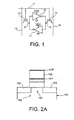
- a conventional SRAM memory cell (SRAM for "static random access memory” or RAM) generally comprises two inverters 10, 11, connected in a so-called “flip-flop” configuration and two access transistors 12, 13 connected to so-called bit lines 15 and 16, and controlled by a word line 17 ( figure 1 ).
- the document US 2006/0284239 A1 discloses a flash memory cell having gate transistors driven by piezoelectric means and having a floating gate.
- the documents US5757696 , US4435786 and US20030042528 disclose SRAM memories comprising floating gate transistors.
- non-volatile memory circuits with improved performance.
- non-volatile memories existing there are for example FLASH type memories, PCM type (PCM for "Phase-Change Memory” or phase change memory).
- PCM type PCM for "Phase-Change Memory” or phase change memory.
- the document [NAT "05] presents, for example, different types of existing nonvolatile memory cells.
- the invention is defined by the memory cell according to claim 1.
- the present invention relates to a random access non-volatile random access memory cell, comprising: at least a first plurality of transistors forming a flip-flop, the first plurality of transistors; of transistors comprising respectively: a gate dielectric and a movable gate, suspended above and disjoint grid dielectric, the gate being located at an adjustable distance from said gate dielectric zone, the transistors being further surmounted by piezoelectric actuating means adapted to move the gate relative to said channel area.
- the piezoelectric actuation means comprise a stack formed of at least one layer of piezoelectric material resting on a first polarization electrode, a second polarization electrode resting on the layer of piezoelectric material.
- the gate may be attached to said first electrode.
- the gate may be in contact with said first electrode.
- the transistors of the first plurality of transistors may have a source zone connected to the second electrode of their respective piezoelectric actuating means.
- the transistors of the first plurality of transistors may advantageously have their respective drain zone connected to the second electrode of their respective piezoelectric actuating means.
- Transistors of the first plurality of transistors are respectively able to adopt: at least a first position in which their gate is located at a first distance from the channel, and to adopt at least a second position in which the gate is located at a second distance from the channel, different from the first distance.
- the random access non-volatile random access memory cell may further comprise supply means capable of supplying the transistors of the first plurality of transistors, and their respective actuating means.
- the transistors of the first plurality of transistors may be adapted respectively to adopt a given position among said first and second positions, and further able to maintain the gate in said given position after stopping or extinction of said supply means.
- the transistors of the first plurality of transistors are respectively adapted to adopt a state in which the piezoelectric actuation means are placed in a given polarization state, and in which the gate is held by means of the piezoelectric actuation means. in contact with the gate dielectric, the transistors of the first plurality of transistors being further adapted to adopt another state in which the piezoelectric actuation means are not polarized, and wherein the gate is held by electrostatic bonding, in contact with the gate dielectric.
- the transistors of the first plurality of transistors may have a variable threshold voltage, which may vary by moving the gate mobile using the piezoelectric actuating means.
- the random access non-volatile random access memory cell according to the invention is capable of adopting several modes of operation including at least one information retention mode contained in the cell, at least one information reading mode contained in FIG. the cell, and at least one information write mode in the cell, the transistors of the first plurality of transistor respectively having a variable threshold voltage.
- the invention also relates to an SRAM memory, comprising a plurality of cells as defined above.
- the invention further relates to a microelectronic device having at least one SRAM memory as defined above.
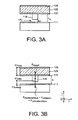
- This transistor rests on a substrate 100, in which a semiconductor zone 102, able to play the role of active zone, has been realized.
- the semiconductor zone 102 comprises a source region 104, a drain region 106, on either side of a channel zone 105 of the transistor.
- a layer 111 of gate dielectric covers the semiconductor zone 102.
- the transistor comprises a suspended gate 116.
- the gate 116 is not integral with, or is not attached to, the gate dielectric layer 111.
- the device is adapted to adopt at least one position in which the gate 116 is located at a distance from the gate dielectric layer 111, so that a space exists between the gate 116 and the gate dielectric layer 111.
- the gate 116 and the gate dielectric layer 111 can be separated by a distance ⁇ (defined on the Figure 2B in a direction parallel to the vector j an orthogonal reference [0; i ; j ; k ]) adjustable or adjustable.
- the gate 116 is suspended or attached by its upper face to piezoelectric actuating means or to a piezoelectric actuator.
- the distance between the gate 116 and the channel 102 can be modulated using the piezoelectric actuating means.
- the piezoelectric actuation means are able to move the gate 116 relative to the channel 105 of the transistor.
- the gate 116 is capable of adopting several positions with respect to the channel 105.
- piezoelectric actuation is meant a displacement of the gate due to a deformation of the piezoelectric layer 125 and its associated electrodes 122, 128 by an inverse piezoelectric effect.
- the piezoelectric actuating means 120 comprise a stack 120 formed of a lower electrode 122 to which the grid 116 can be attached, a layer of piezoelectric material 125 resting on the lower electrode 122, and an upper electrode 128 resting on the layer of piezoelectric material 125.
- the device may also comprise one or more elements 121b, 121c, supporting the stack 120 of the piezoelectric actuator, located on the periphery of the latter ( Figure 2B ). Plots (not shown on the Figures 2A-2B ) are also provided for making the contacts of the transistor. One or more conductive pads may also be provided for making the contacts of the piezoelectric actuator. Conductive pads may be provided for respectively connecting or electrically connecting source area 104 to source biasing means, drain area 106 to drain biasing means 106, gate 116, and lower electrode 122. from the stack 120 to polarization means of the gate and the lower electrode 122, the upper electrode 128 of the actuator to polarization means of the piezoelectric actuator.
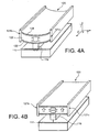
- the device can adopt a so-called "rest” position in which the stack 120 is suspended above and at a so-called “rest” height h0 of the gate dielectric layer 111.
- the gate 116 In the rest position, the gate 116 is at a so-called “rest” distance ⁇ 0 from the dielectric 111, so that a gap 170 is located between the gate 116 and the gate dielectric zone 111.
- the piezoelectric layer 125 may be flat in the rest position. In the rest position, the supply of the actuating means and the transistor is off, so that all the polarizations are at a zero potential ( figure 3A ).
- the piezoelectric actuation means can actuate the gate 116, and allow to move the latter. According to the direction of the external electric field applied to it by means of the electrodes 122, 128, this piezoelectric layer 125 is able to compress or to relax, and to thereby move the gate 116 attached thereto.
- an electrostatic attraction effect resulting from the potential difference between the gate 116 and the transistor channel 105 is capable of being implemented.
- This effect of electrostatic attraction results in an electrostatic force tending to bring the gate 116 closer to the channel 105 of the transistor, and which can make it possible to put the gate 116 and the gate dielectric 111 into contact.
- adhesion or also called molecular bonding can also be implemented.
- Molecular bonding In particular, the Van der Waals type can be exerted between the lower face of the gate 116 and the gate dielectric surface 111.
- the implementation of this additional force depends in particular on the flatness of the lower face of the gate 116 and the facing surface of gate dielectric 111, as well as a suitable dimensioning of the elements of the structure.
- the implementation of the adhesion or molecular bonding force is described for example in the following documents: Asghar Ramezani et al. : "Influence of Van Der Waals Force on the Pull-In Parameters of Cantilever Type Nanoscale Electrostatic Actuators", Microsystem Technologies, 2006, vol. 12, pp.
- the implementation of the adhesion force or molecular bonding allows to give the device a non-volatile operation. The latter is likely to remain in a given position during the power off and polarizations of the actuator and the transistor. When the polarizations are off, the gate 116 is capable of being kept in contact with the gate dielectric 111. When the transistor is biased again, it is likely to adopt the same mode of operation as that in which it had been left before stopping polarizations.
- the device is placed in a state of polarization different from that of the rest position and for which the device adopts a first position in which the gate 116 is not in contact with the surface of the gate dielectric layer 111, the gate 116 being maintained at a non-zero distance ⁇ from the gate dielectric layer 111.
- the piezoelectric means are placed in a suitable state of polarization, a non-zero potential being applied to the electrodes.
- the 116 suspended gate of the transistor can then be subjected to four forces, a first or electrostatic electrostatic force F due to the potential difference present between the gate and the surface of the transistor channel, a second force or piezoelectric force piezoelectric F, generated by the potential difference applied between the two electrodes 122, 128 of polarization of the piezoelectric layer, a third force or restoring force F return , corresponding to the stiffness of the mechanical support of the gate 116, that is to say at the stiffness of the stack formed of the piezoelectric layer 125 and the electrodes 122, 128, and the layer or insulating elements supporting the stack, a fourth force of molecular bonding or force Accession F adhesion, particularly resultant of the forces Van Der Waals acting between the underside of the gate 116 located next to the dielectric layer 111 gate and the surface of the dielectric layer 111 of gate.
- the state of polarization of the electrodes of the actuating means is adapted so that: F electrostatic +
- a different polarization of the piezoelectric actuating means may allow the latter to be displaced.
- the fourth force can become significant when ⁇ is made weak, for example less than 1 nm.
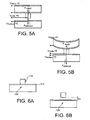
- a collage ( Figure 4A ) of the gate 116 on the dielectric layer 111 can be realized when the following condition is implemented: F electrostatic +
- a predetermined dimensioning of the elements of the device, and a suitable polarization can make it possible to achieve this condition.
- the gate 116 In the bonding position, the gate 116 is in contact with the surface of the gate dielectric 111.
- the gate 116 of the transistor is subjected, as a first approximation, to the four forces presented above for the gluing mechanism.
- a detachment ( Figure 4B ) of the gate 116 is implemented when the following condition is satisfied: F piezoelectric
- a predetermined dimensioning of the elements of the device and a suitable bias can make it possible to achieve this condition.
- the gate 116 can be maintained, after stopping the polarizations, in a position in which it was before this stop.
- the gate 116 is subjected only to the restoring forces of the structure and adhesion to the surface of the gate dielectric 111.
- the piezoelectric and electrostatic forces dependent on the applied potential differences become zero.
- Two cases of maintaining the position of the gate 116 may for example be made.
- the adhesion forces are low compared to the restoring forces, which keeps the gate 116 in the rest position ( Figure 5A ).
- low displacement means a small displacement with respect to the distance ⁇ 0 of rest.
- a predetermined dimensioning of the elements of the device in particular a stiffness of the stack and of the piezoelectric layer adapted as well as a distance ⁇ 0 of rest chosen can make it possible to realize this condition.
- the piezoelectric actuation means and the support elements of the stack have dimensions and a composition adapted to achieve a stiffness at the edge of the stack that allows to fulfill the condition of maintaining the grid in said second case which has just been given.
- the gate 116 is likely to remain in its position stuck against the dielectric 111, with the aid of adhesion forces that vary greatly with the distance separating the gate 116 of the gate dielectric 111, more than the restoring forces.
- the restoring forces can be proportional to this distance while the adhesion forces are inversely proportional to a power of this distance, for example inversely proportional to the cube of this distance for Van der Waals forces.
- the threshold voltage V T of the transistor may be modulated by varying the insulating thickness between the gate 116 and the channel 105 of the transistor.
- the gate 116 of the transistor is glued against or in contact with the gate dielectric 111.
- the insulating thickness between the gate 116 and the channel 105 thus corresponds to the thickness e 1 of the gate dielectric layer.
- the transistor has a first threshold voltage V T1 .
- the gate 116 of the transistor is located at a distance ⁇ from the gate dielectric 111 116.
- the insulating thickness between the gate 116 and the channel 105 corresponds to the thickness of the gate dielectric layer added to a thickness ⁇ d. air between the gate 116 and the gate dielectric 111.
- the transistor has a second threshold voltage V T2 .
- the transistor of the device has a threshold voltage that can be dynamically changed, and have for example a first threshold voltage V T1 which can be for example low when the transistor is in the on state and a second threshold voltage V T2 for example such that V T2 > V T1 and which can be high when the transistor is in the off state.
- V T1 which can be for example low when the transistor is in the on state
- V T2 for example such that V T2 > V T1 and which can be high when the transistor is in the off state.
- a characteristic curve representative of the drain current as a function of the potential applied to the gate is given on the Figure 6C .
- a first portion of the curve C 12 corresponds to a position in which the gate is glued against the gate dielectric 111, while another portion of the curve C 11 corresponds to a position in which the gate is peeled off or in a position of rest.
- Such a device is likely to operate at variable threshold voltage and thus to be able to have a slope below a threshold below the limit of 60mV / dec conventional architectures of MOS transistor single or double grids.
- the starting material is a semiconductor-on-insulator type substrate, such as an SOI (Silicon On Insulator) substrate.
- SOI Silicon On Insulator
- the method is not limited to such a substrate and can be adapted for example to an embodiment on a solid substrate or on a constrained substrate.
- the starting substrate may be formed of a layer 200 of semiconductor material, for example monocrystalline silicon, surmounted by a layer 201 of insulating material, for example silicon oxide, on which a thin layer of material rests. semiconductor, for example monocrystalline silicon, and provided to form an active layer.
- the thin layer of semiconductor material is defined, for example by etching, at least one semiconductor zone 202.
- active source zones 204 and drain zones 206 on either side of a channel zone 205, can be produced.
- the semiconductor zone 202 is covered with a layer intended to form a gate dielectric zone 211 surmounted by a first sacrificial layer 213.
- the first sacrificial layer 213 is intended to be removed later in order to disconnect the future transistor gate of the gate dielectric layer 211, and make a gap between this future gate and the grid dielectric zone 211.
- the gate dielectric zone 211 may for example be based on silicon oxide and produced by thermal oxidation of a silicon layer or by deposition of a dielectric material having a high dielectric constant ("high-k"). Anglo-Saxon terminology) such as HfO 2 or Al 2 O 3 or HfSiO x .
- the dielectric zone 211 may have a thickness of, for example, between 1 nanometer and 10 nanometers, for example of the order of 2 nanometers.
- the sacrificial layer 213 is based on a material that can be etched selectively relative to the other materials of the structure.
- the sacrificial layer 213 is based on a material capable of being etched selectively with respect, in particular, to the dielectric 211 and with respect to the future gate.
- the choice of the material of the sacrificial layer 213 may also be provided as a function of that of the materials of the piezoelectric layer and support elements of this layer intended to be produced later, so that it can be etched selectively with respect to this layer. piezoelectric and these support elements.
- the first sacrificial layer 213 may for example be Ge-based or SiGe-based. According to another example, the first sacrificial layer 213 may be based on SiO 2 in the case where the gate dielectric is based on a "high-k" material.
- the sacrificial layer 213 may have a thickness for example between several nanometers and several tens of nanometers, for example of the order of 4 nanometers ( Figure 7A ).
- a gate 216 based on at least one gate material, for example metal such as TiN, or semiconductor for example such as polycrystalline silicon, or a stack formed of at least one metal layer and at least one semiconductor layer.
- the gate 216 may have a thickness for example between 10 nanometers and 1 micrometer, for example of the order of 50 nanometers.
- the gate 216 may have a critical dimension dc for example between several nanometers and several hundred nanometers, for example of the order of 40 nanometers. (defined on the Figure 7A in a direction parallel to the plane [0; i ; k ] an orthogonal reference [0; i ; j ; k ]).
- Areas of extension can then be made, for example by ion implantation.
- insulating spacers 217a, 217b are formed on either side of the grid 216, based on an insulating material, for example such as SiO 2 or Si 3 N 4 or a stack of these two materials. .
- the semiconductor zone 202 can then be doped, for example by implantation, so as to produce the source 204 and drain 206 zones.
- the structure is then covered with a second sacrificial layer 219.
- This second sacrificial layer 219 may be made by deposition and then removed in an area situated above the grid 216.
- the removal of the second sacrificial layer 219 from above the grid can be carried out by planarization CMP (CMP for Chemical Mechanical Planarization) until revealing the upper face of the grid 216.
- CMP Chemical Mechanical Planarization
- the second sacrificial layer 219 can be based on a material that can be etched selectively relative to the others materials of the structure.
- the second sacrificial layer 219 may be based on a material that can be etched selectively with respect, in particular, to the gate dielectric 211 and with respect to the future gate.
- the choice of the material of the second sacrificial layer 219 can also be provided as a function of that of the materials of a piezoelectric layer and of the support elements of this piezoelectric layer intended to be produced later, so that it can be etched selectively with respect to to this piezoelectric layer and these support elements.
- the second sacrificial layer 219 may for example be based on Si.
- the sacrificial layer may be based on the same material as the first sacrificial layer, for example based on SiGe or Ge.
- the second sacrificial layer 219 may optionally be based on SiO 2, especially in the case where the gate dielectric is based on a "high-k" material.
- the second sacrificial layer 219 may be based on the same material as the first sacrificial layer 213 ( Figure 7C ).
- a stack of layers is then deposited from which piezoelectric actuation means are intended to be defined.
- This stack may be formed of a layer 225 based on a piezoelectric material such as for example AlN, PZT, LiNbO 3 or LiTaO 3 , PMN-PT, LiNbO 3 , LiTaO 3 interposed between two conductive layers 222, 228 intended to act as polarization electrodes of the piezoelectric layer 225.
- a piezoelectric material such as for example AlN, PZT, LiNbO 3 or LiTaO 3 , PMN-PT, LiNbO 3 , LiTaO 3 interposed between two conductive layers 222, 228 intended to act as polarization electrodes of the piezoelectric layer 225.
- the conductive layers 222, 228 may be formed of a metallic material, chosen according to the material used for the piezoelectric layer 225, and which may be, for example, Mo, Ti or Pt.
- the piezoelectric layer 225 may, for its part, it can be achieved by depositing a piezoelectric material or by transfer of this material on the conductive layer 222, using a gluing mechanism. A transfer advantageously makes it possible to form a layer of monocrystalline piezoelectric material.
- the choice of the material of the conductive layers 222, 228 and the material of the piezoelectric layer 225 is provided so as to optimize the piezoelectric properties, and in particular the ability of the layer 225 to deform under the action of a voltage. electric imposed by the electrodes, preferably low or the lowest possible.
- the conductive layers 222 and 228 may be based on Mo.
- the layer of piezoelectric material may have a thickness for example between 100 nanometers and 1 micrometer, for example of the order of 150 nanometers.
- the conductive layers 222, 228 can have a thickness of between 10 nanometers and 100 nanometers, for example of the order of 10 nanometers.
- At least one pattern is then produced, for example by photolithography and etching of the stack of layers 222, 225, 228, and of the second sacrificial layer 219, so as to define a block in which, a lower electrode 222a, a block of piezoelectric material 225a on the lower electrode, and an upper electrode 228a on the block 225a of piezoelectric material are made.
- the formed block may have a rectangular pattern of width W and length L (the length L being defined on the Figure 7D in a direction parallel to the vector i orthogonal reference [0; i ; j ; k ]).
- At least one insulating layer 231 is formed on the structure, for example based on SiO 2 or Si 3 N 4 , or a stack of insulating layers, for example formed of a thin layer based on Si 3 N 4 . covered by a layer based on SiO 2 .
- this insulating layer 231 or this stack is then removed, for example by etching, in an area situated above the upper electrode 228a.
- the remaining portions of the insulating layer 231 surround the transistor as well as the stack comprising the piezoelectric block 225a and the electrodes 222a, 228a.
- the remaining portions of the insulating layer 231 thus form a support or a reinforcing element, able to support the stack of layers 222a, 225a, 228a of the piezoelectric actuator.
- the material of the insulating layer 231 may be chosen to have a rigidity greater than that of the piezoelectric material 225, so as to promote the displacement of the gate induced by the deformation of the piezoelectric layer.
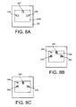
- FIGS. 7E and 8A We then define ( figures 7E and 8A ), on either side of the gate of the transistor, for example by photolithography and through the stack of layers 228a, 225a, 222a, sacrificial layers 219, 213, and the gate dielectric zone 211, openings 233, 235, respectively revealing the source zone 204 and the drain zone 206 defined in the semiconductor zone 202. At least one opening 237 is also made through the layers 228a, 225a, 222a, so as to reveal the gate 216 or the first conductive layer 222.
- the openings 233, 235, 237 may be provided with a diameter or critical dimension d1 (defined on the figure 7F in a direction parallel to the plane [0; i ; k ]).
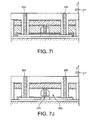
- the openings 233, 235 and 237 are filled with an insulating material 238, for example SiO 2 ( figures 7G ). Then, a chemical mechanical polishing (CMP) of the layer of insulating material 238 can be carried out.
- CMP chemical mechanical polishing
- holes 243, 245 and 247 of diameter or critical dimension d.sub.2 (defined in FIG. figure 7H in a direction parallel to the plane [0; i ; k ]), holes 243, 245 and 247 respectively reveal the source zone 204, the drain zone 206, and the grid 216 or the first conductive layer 222 (FIG. Figure 7G ).
- the holes 243, 245 and 247, 249 are then filled with at least one conductive material, for example a metal such as tungsten, so as to form conductive pads 253, 255 and 257, 259 in the holes. 243, 245 and 247, 249.
- the conductive pads 253, 255, 257, 259 are respectively in contact with the source zone 204, the drain zone 206, with the gate 216 or with the lower electrode 222a, and with the upper electrode 228a ( figures 7I and 8C ).
- At least one opening 261 is then made in the block, passing through the stack 220 and the sacrificial layers 213, 219.
- the opening 261 may be made, for example by means of photolithography and etching steps ( figure 8D ).
- a partial or total withdrawal ( figure 7J ) sacrificial layers 213, 219, so as to separate the gate 216 from the gate dielectric 211.
- the removal of the sacrificial layers 213, 219 can be achieved for example by delocalized plasma etching, the plasma being formed in a given room and relocated in another chamber in which is placed the device comprising the sacrificial layers to be removed.
- the removal of the first sacrificial layer 213 is performed so as to create a space 270 between the gate 216 and the gate dielectric layer 211.
- the shrinkage can be achieved by selective etching of the first layer vis-a-vis the grid, the gate dielectric.
- the shrinkage may for example be achieved by selective etching of a first semiconductor sacrificial layer, for example Si, vis-à-vis a Ti grid, of a SiO 2 -based gate dielectric.
- the etching may also be selective with respect to spacers and / or support elements, for example when they are based on Si 3 N 4 .
- the second sacrificial layer 219 can also be removed so as to form a space around or around the grid 216.
- the removal can be achieved by selective etching of the second layer vis-à-vis the grid, the gate dielectric and support elements.
- the shrinkage can be achieved, for example, by selective etching of a first SiGe sacrificial layer, with respect to a Ti grid, of an SiO 2 -based gate dielectric and of spacers and / or support elements based on Si 3 N 4 .
- the removal of the two sacrificial layers 213 and 219 can be performed at the same time.
- a withdrawal, possibly total, of the second sacrificial layer 219 can in turn be performed so as to make a cavity 280 around the gate 216.
- the gate 216 is maintained or attached by its upper face to the lower electrode 222a of the actuator ( figure 7J ).
- the upper electrode 228a resting on the piezoelectric layer 225 is not connected or electrically connected to any of the contact pads 253, 255, 257, of source contact, of drain contact , and gate contact 257.
- the upper electrode 228a can be connected or subsequently electrically connected to the source pad 253, or the drain pad 255, during subsequent steps of a process part commonly referred to as "back-end steps" during of which, a plurality of levels are realized metal interconnections of integrated circuit components.
- the support layer 231 can be etched again so as to release sides of the stack formed of the electrodes 222a, 228a and the piezoelectric block 225a.
- the etching can be performed to release two sides, for example the two longer sides of the rectangle to allow the layer piezoelectric 225a to deform more easily, under the action of a polarization.
- the stack formed of the electrodes 222a, 228a and the piezoelectric block 225a is held in suspension above the substrate 200 by means of two insulating elements or support blocks 231b, 231c, insulating formed by etching the insulating layer 231 .
- gate, openings 333, 335 respectively revealing the source zone 204, the drain zone 206 defined in the semiconductor zone 202, and the gate 216.
- At least one opening 337 is also formed, revealing the gate zone 216. or the first conductive layer 222a.
- the opening 333 revealing the source zone 204 may be provided with a diameter or a critical dimension greater than that of the other openings 335, 337 ( figure 10A ).
- the openings 333, 335 and 337 are then filled with an insulating material 238, for example SiO 2 .
- holes 343, 345 and 347 are each made with a diameter smaller than that, or with a critical dimension d2 smaller than that of apertures 333, 335 and 337 ( Figures 9A and 10B ).
- the mouth 344 is then widened by a hole formed opposite an active zone, for example the mouth 344 of the hole 343 revealing the source zone 204.
- the mouth of the hole 343 is enlarged so as to reveal a part the upper face of the upper electrode 228a of the piezoelectric actuator. This enlargement is carried out so as to maintain an insulating zone 351 or a isolating spacer 351 between the hole 343 and the lower electrode 222a of the actuator.
- the holes 343, 345 and 347 are then filled with at least one conductive material, for example a metal such as tungsten, so as to form metal studs 353, 355 and 357 in the holes 343, 345. and 347.
- the metal studs 355 and 357 are respectively in contact with the drain zone, and with the gate 216.
- the stud 353 formed of the hole 343 with enlarged mouth and filled with metal, is in contact with the upper electrode 228a and the source zone 204 ( Figures 9C and 10C ).
- At least one opening is then made, revealing the sacrificial layers 213, 219.
- the opening may be made so as to pass through the sacrificial layers 213, 219, or alternatively, be made on the periphery of the structure, but in such a way as to reveal the sacrificial layers 213, 219.
- the sacrificial layers 213, 219 are etched through the opening so as to remove these sacrificial layers 213, 219, and in particular to separate the gate 216 from the gate dielectric 211.
- a space 270 between the gate 216 and the gate dielectric layer 211 is thus formed.
- a cavity 280 all around the gate 216 may also be formed following the removal of the second sacrificial layer 219, for example by selective isotropic etching ( Figure 9D ).
- a stud in contact with the source zone 204 and the second conductive layer 222 of the upper electrode 222a has been produced. It is possible, by performing a similar process, to form a pad in contact with the drain zone 206 and the second conductive layer 222 of the upper electrode 222a.
- the holes 343, 345 and 347 are then filled with a metal, for example tungsten, so as to form conductive pads 453, 455 and 457 in the holes 343, 345 and 347.
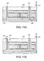
- the conductive pads 453 , 455 and 457 are respectively in contact with the source zone 204, the drain zone 206, and with the gate 216 or the first electrode 222 (FIG. Figures 11A and 12A ).
- an additional hole 444 is then made in the insulating material 239 so as to reveal a portion of the upper electrode 228a and flanks of the stud 453.
- the additional hole 444 is constructed so that an insulating area 459 is kept between the pad 453 and the lower electrode 222a ( Figure 11B ).
- the hole 444 is filled with a metal, for example such as tungsten, so as to form a metal zone 454 for extending the stud 453, in contact with the upper electrode 228a of the metal.
- a metal for example such as tungsten
- the sacrificial layers 213, 219 are etched so as to effect removal of these sacrificial layers 213, 219, and to separate the gate 216 from the gate dielectric 211.
- the second sacrificial layer 219 can also be removed so as to form a space around or around the grid 216.
- the removal of the two layers sacrificial 213 and 219 can be realized at the same time.
- the gate 216 is maintained or attached by its upper face to the lower electrode 222a of the actuator.
- a pad in contact with the source zone 204 and the second conductive layer 222 of the electrode upper 222a has been realized. It is possible, by performing a similar process, to form a pad in contact with the drain zone 206 and the second conductive layer 222 of the upper electrode 222a.
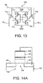
- FIG. figure 13 A first example of a random access memory cell 500 according to the invention is illustrated in FIG. figure 13 .
- This memory cell 500 is a SRAM static memory cell type 6T, that is to say provided with 6 transistors.
- the cell 500 comprises a first plurality of transistors forming a first inverter and a second inverter, connected in a flip-flop configuration or commonly called "flip-flop".
- the first load transistors TL T and the conduction transistor TD T form the first inverter of the flip-flop, while the second load transistors TL F and the conduction transistor TD F form the second inverter of the flip-flop.
- the first plurality of transistors may be formed of a first load transistor TL T , as well as a second load transistor TL F.
- the load transistors TL T and TL F may be, for example of the P type.
- the cell 500 may also be provided with a first conduction transistor TD T and a second conduction transistor TD F , for example of the type NOT.
- the transistors TL T , TL F , TD T , TD F of the cell forming the flip-flop are similar to that previously described in connection with the Figures 2A-2B , equipped with a mobile suspended grid and means piezoelectric actuators for moving the gate.
- the cell also comprises access transistors TA T and TA F , for example of the NMOS type.
- connections in the cell may be similar to those of a conventional 6T memory cell.
- the gate of the second load transistor TL F is connected to that of the second conduction transistor TD F , and to a first storage node T of the cell 500.
- the gate of the first load transistor TL T is connected to that of the first conduction transistor TD T , and a second storage node F.
- the sources of the load transistors TL T , TL F can be connected to one another and to a supply voltage VDD, whereas the drain of the first load transistor TL T is connected to the first node T, the drain the second load transistor TL F being connected to the second node F.
- the load transistors TL T and TL F connected to the supply voltage VDD, have in this example the function of maintaining a logic level '1', for example equal to a voltage VDD, to one or the other storage nodes T or F, for example at the first node T, as a function of the logic value stored in the cell 500.
- the conduction transistors TD T and TD F connected to the ground of the GND cell, have the role of maintain a level logic '0', equal to GND, to one or the other of the storage nodes according to the stored logic value.
- the two access transistors TA T and TA F are provided, depending on the manner in which they are polarized, to allow access to the potentials of the storage nodes during a read or write cycle, and to block access to cell 300, when cell 300 is in an information retention mode.
- the first access transistor TA T and the second access transistor TA F each comprise a gate connected to a word line WL.
- the source of the first access transistor TA T is connected to a first bit line BL T
- the source of the second access transistor TA F is connected to a second bit line BL F.
- the drain of the first access transistor TA T is connected to the first storage node T while the drain of the second access transistor TA F is connected to the second storage node F.
- Actuation of the suspended gate of the transistors TD T , TD F , TL T and TL F by means of piezoelectric means modulates their threshold voltage V T.
- the piezoelectric actuation means make it possible to give the cell 500 a non-volatile operation, insofar as the movable gate actuated by such means is able to remain in position, even after extinction of the supply voltage VDD.
- the latter can be reset or reset when it is restarted in the state in which it was before extinguishing.
- TD transistors T , TD F , TL T and TL F two configurations can be implemented.
- the upper electrode 128 of the piezoelectric actuating means and the source 104 of the transistor are connected together.
- the transistors TD T , TD F , TL T and TL F , of a cell 600 similar to the cell 500 have this first configuration.
- a cell 700 similar to the cell 500 comprises TD transistors T , TD F , TL T and TL F , adopting the second configuration.
- the potential difference between the gate and the source for the first conduction transistor TD T may be 0V while the potential difference between grid and the source of the second TD F conduction transistor is + VDD, giving a total potential difference of 1xVDD.
- the potential difference between gate and drain for the first conduction transistor TD T may be -VDD while the potential difference between gate and the drain of the second conduction transistor TD F is + VDD, which makes it possible to obtain a total potential difference between the two conduction transistors of 2xVDD, greater than in the first configuration. It is the same for the load transistors TL T and TL F.
- Transistors TD T , TD F , TL T , TL F are connected according to the second configuration with their respective piezoelectric actuators.
- the respective threshold voltage of the transistors is capable of being modulated according to the mode, retention or reading or writing, in which the cell 700 is located.
- the word line WL can be maintained at ground potential GND.
- the access transistors TA T and TA F are in a blocked state and the information stored in the cell 700 is isolated from the bit lines BL T and BL F.
- the cell 700 is configured so that in the retention mode, the threshold voltage of the first conduction transistor TD T is increased by + ⁇ VT N with respect to a threshold voltage value VT N , while the threshold voltage of the second transistor TL F is increased by + ⁇
- the cell 700 is also configured so that in the retention mode, the threshold voltage of the second conduction transistor TO F is equal to a threshold voltage value VT N , while the threshold voltage of the first load transistor TL T is equal to a threshold voltage value
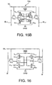
- FIG. figure 16 This configuration of the threshold voltages of transistors TD T , TD F , TL T , TL F when cell 700 is in retention mode, is illustrated on FIG. figure 16 .
- Such a configuration makes it possible to obtain an increased retention stability RNM of the cell 700 and, on the other hand, reduced leakage currents.
- Increasing the threshold voltage of the first conduction transistor TD T and the second load transistor TL F respectively makes it possible to reduce their current below the threshold and to limit the discharge of the storage node T and the load of the storage node F in a case for example where it is desired to maintain a logic level '1' in the first node T and a logic level '0' in the second node.
- the low threshold voltage of the first load transistor TL T and the second conduction transistor TD F make it possible to increase their conduction current, which reinforces the load of the node T and the discharge of the node F.
- the bit lines BL T and BL F may be loaded at an equal potential V DD. Then in read mode, the word line WL is biased to the potential VDD, to allow access to the storage nodes T and F of the cell 700.
- the stability of the cell 700 in read mode depends in particular on the value of the potential the storage node F which is at logic level '0', for example the second node F. This voltage must preferably remain lower than the switching voltage of the inverter connected to the logical level storage node '1', for example the first node T. This condition is related to the voltage divider between the second bit line BL F and the ground GND of the cell 700, formed by the second access transistor TA F and the second conduction transistor TD F connected to the logical level node '0'.
- this cell is implemented so that the linear current flowing through the second conduction transistor TD F is greater than the saturation current of the second access transistor TA F.
- the current gain ratio between the conduction and access transistors, is typically of the order of 2. For transistors provided with a grid having a critical dimension of less than 65 nm, this ratio tends to 3.
- the transistors of FIG. conduction TD T and TD F , and load TL T and TL F , with a movable gate and piezoelectric actuation of the gate allow to give the memory cell 700 a current gain ratio greater than that of a cell SRAM 6T according to the prior art and of the same size.
- the mechanical deformation of the piezoelectric material of the TD T and TD F conduction transistors and of the TL T and TL F charges makes it possible to modulate their threshold voltage favorably, thereby enhancing the stability of the read-only cell (SNM).
- the threshold voltage of the first conduction transistor TD T and the second load transistor TL F is increased, which allows, respectively, to limit the discharge of the node T and to decrease the load of the node F.
- the threshold voltage of the first load transistor TL T and that of the second conduction transistor TD F are also low, which makes it possible to increase their conduction current and to increase the load of the first storage node T and the discharge of the second storage node F, in a case for example where the first node T is intended to be at a logic level '1' while the node F is at a logic level '0'.
- the latter increases with respect to the conventional case, where the stored information does not affect the threshold voltage of the transistors by increasing the conduction current of the second conduction transistor of the transistor TD F related to the decrease of its voltage.
- one of the two bit lines for example the second bit line BL F may be at a potential V DD, while the complementary bit line BL F may be biased to the potential GND mass.
- the word line WL is biased to a VDD potential in order to write to the cell 700.
- the switchover of the logic information contained in the memory cell 700 is accompanied by a variation of the threshold voltages of the conduction transistors TD T and TD F and of the load TL T and TL F , as illustrated in FIGS. Figures 17A-17B .
- the cell 700 is configured so that when it goes into a write mode, the threshold voltage of the second conduction transistor TD F is likely to increase, and go from VT N to (VT N + ⁇ VT N ), while the threshold voltage of the first load transistor TL T is likely to increase, by + ⁇
- the transistors TD F and TL T go from a glued state to a grid state unstuck
- the cell 700 is also configured so that in the retention mode, the threshold voltage of the first conduction transistor TD T is likely to decrease, and go from (VT N + ⁇ VT N ) to (VT N ), while the voltage threshold of the second load transistor TL F is decreased by + ⁇
- This modulation of the threshold voltage is relative to the polarization change of the piezoelectric actuators associated with each of the transistors TL T , TL F , TD T , TD F. These polarization changes will result in a complementary deformation of the materials piezoelectric, modulating the potential difference between the gate and the channel surface of the transistors.
- the memory cell 700 In "start" mode, the memory cell 700 is powered up.
- the storage nodes of the cell T and F switch voltage according to the last stored state, which is maintained by a suitable difference between the restoring forces on the layers of piezoelectric materials and the bonding forces at the interface grid / gate dielectric of the transistors TL T , TL F , TD T and TD F.
- the figure 18 illustrates a start-up phase of the memory cell 700.
- the curve C0 represents the evolution of the supply potential
- the curves C1 and C2 respectively represent the evolution of the potential at the first node T and the evolution the potential at the second node F.
- the cell 700 is not powered.
- the cell 700 is fed again (curve C0 arriving gradually at the value VDD).
- the potential of the first node T finds a value for example equal to VDD corresponding to a state logic "1" (increasing curve C1 reaching the value VDD) while the potential of the second node F finds a value for example equal to GND or 0 volts corresponding to a logic state '0' (curve C2).
- the information that was present in the nodes T and F before stopping the power supply of the cell 700, is preserved insofar as the nodes T and F find, without a writing operation, being necessary. potential they had prior to extinction.
- a modulation of the threshold voltage of the conduction transistors TD T , TD F , and of the load TL T and TL F as implemented in the cell 700 makes it possible to improve the static noise margin SNM of the order of 50mV, or more than 25%, and reduce leakage currents by more than compared to the standard 6T cell.
- the current I CELL of the cell 700 is also improved with respect to the cell of the prior art.
Landscapes
- Engineering & Computer Science (AREA)
- Chemical & Material Sciences (AREA)
- Nanotechnology (AREA)
- Physics & Mathematics (AREA)
- Mathematical Physics (AREA)
- Theoretical Computer Science (AREA)
- Crystallography & Structural Chemistry (AREA)
- Semiconductor Memories (AREA)
- Insulated Gate Type Field-Effect Transistor (AREA)
- Semiconductor Integrated Circuits (AREA)
- Static Random-Access Memory (AREA)
- Micromachines (AREA)
Claims (12)
- Nicht-flüchtige Speicherzelle mit wahlfreiem Zugriff (Random-Access-Speicher), welche umfasst:- wenigstens eine erste Mehrzahl von eine Kippschaltung bildenden Transistoren (TLT, TLF, TDT, TDF), wobei die Transistoren der ersten Mehrzahl von Transistoren jeweils aufweisen: ein Gate-Dielektrikum und ein mobiles bzw. bewegliches Gate (116, 216), das über dem Gate-Dielektrikum hängend angeordnet ist, derart dass das Gate in einer einstellbaren Entfernung von der genannten Gate-Dielektrikumszone angeordnet ist, wobei des weiteren über den Transistoren der ersten Mehrzahl von Transistoren jeweils piezoelektrische Betätigungsmittel angebracht sind, die das Gate relativ gegenüber der genannten Kanalzone (105) verschieben können, und wobei die piezoelektrischen Betätigungsmittel einen Schichtstapel (120, 220) umfassen, der aus wenigstens einer Schicht (125, 225) aus piezoelektrischem Material gebildet wird, die auf einer ersten Vorspannelektrode (122, 222) aufruht, und aus einer auf der Schicht aus piezoelektrischem Material ruhenden zweiten Vorspann-Elektrode, und wobei ferner die Transistoren der ersten Mehrzahl von Transistoren jeweils wenigstens eine erste Stellung einnehmen können, in welcher ihr Gate (116) von dem Gate-Dielektrikum getrennt und in einem ersten Abstand von dem Kanal liegt, und wenigstens eine zweite Stellung einnehmen können, in welcher das genannte Gate in einem zweiten, von dem ersten Abstand verschiedenen Abstand von dem Kanal liegt, wobei die Speicherzelle dadurch gekennzeichnet ist, dass in der genannten zweiten Stellung das Gate in Berührung mit der Gate-Dielektrikums-Zone gehalten wird, und zwar- mit Hilfe der piezoelektrischen Betätigungsmittel in deren vorgespanntem Zustand, oder- mittels elektrostatischer Klebung, im nicht-vorgespannten Zustand der piezoelektrischen Betätigungsmittel.
- Nicht-flüchtige Speicherzelle mit wahlfreiem Zugriff (Random-Access-Speicherzelle) nach Anspruch 1, bei welcher das Gate an der genannten ersten Elektrode (122, 222) befestigt ist.
- Nicht-flüchtige Speicherzelle mit wahlfreiem Zugriff (Random-Access-Speicherzelle) nach Anspruch 1 oder 2, bei welcher das Gate mit der genannten ersten Elektrode (122, 222) in Kontakt steht.
- Nicht-flüchtige Speicherzelle mit wahlfreiem Zugriff (Random-Access-Speicherzelle) nach einem der Ansprüche 1 bis 3, bei welcher die Transistoren der ersten Mehrzahl von Transistoren eine Source-Zone (104) aufweisen, die mit der zweiten Elektrode (128) ihrer betreffenden piezo-elektrischen Betätigungsmittel verbunden ist.
- Nicht-flüchtige Speicherzelle mit wahlfreiem Zugriff (Random-Access-Speicherzelle) nach einem der Ansprüche 1 bis 3, bei welcher die Transistoren der ersten Mehrzahl von Transistoren eine Drain-Zone (106) aufweisen, die mit der zweiten Elektrode (128) ihrer betreffenden piezoelektrischen Betätigungmittel verbunden ist.
- Nicht-flüchtige Speicherzelle mit wahlfreiem Zugriff (Random-Access-Speicherzelle) nach einem der Ansprüche 1 bis 5, welche des weiteren Mittel zur Stromversorgung der Transistoren der ersten Mehrzahl von Transistoren und ihrer betreffenden Betätigungsmittel umfasst, wobei die Transistoren der ersten Mehrzahl von Transistoren jeweils eine von den genannten ersten und zweiten Stellungen einnehmen können und des weiteren nach dem Anhalten bzw. der Abschaltung der genannten Stromversorgunnsmittel das Gate in der genannten jeweiligen Stellung halten können.
- Nicht-flüchtige Speicherzelle mit wahlfreiem Zugriff (Random-Access-Speicherzelle) nach einem der Ansprüche 1 bis 6, in welcher die Transistoren der ersten Mehrzahl von Transistoren eine variable Schwellwertspannung besitzen, die durch Verschieben des beweglichen Gates (116, 216) mit Hilfe der piezoelektrischen Betätigungsmittel variiet werden kann.
- Nicht-flüchtige Speicherzelle mit wahlfreiem Zugriff (Random-Access-Speicherzelle) nach einem der Ansprüche 1 bis7, welche mehrere Funktions-Betriebsarten einnehmen kann, darunter wenigstens eine Betriebsart der bewahrenden Erhaltung von Informationsgehalt der Zelle, wenigstens eine Betriebsart des Lesens von in der Zelle enthaltener Information, und wenigstens eine Betriebsart des Schreibens in die Zelle, wobei die Transistoren der ersten Mehrzahl von Transistoren jeweils eine variable Schwellwertspannung aufweisen.
- Nicht-flüchtige Speicherzelle mit wahlfreiem Zugriff (Random-Access-Speicherzelle) nach einem der Ansprüche 1 bis 8, in welcher die genannte erste Mehrzahl von Transistoren umfasst:- einen ersten Ladetransistor (TLT) und einen zweiten Ladetransistor (TLF),- einen ersten Leitungstransistor (TDT) und einen zweiten Leitungstransistor (TDF).
- Nicht-flüchtige Speicherzelle mit wahlfreiem Zugriff (Random-Access-Speicherzelle) nach einem der Ansprüche 1 bis 9, welche wenigstens einen ersten Zugangstransistor (TAT) und wenigstens einen zweiten Zugangstransistor (TAF) umfasst, die jeweils zwischen einer eresten Bit-Leitung (BLT) und einem ersten Speicherknoten (T) sowie zwischen einer zweiten Bitleitung (BF) und einem zweiten Speicherknoten angeordnet sind.
- SRAMSpeicher, welcher eine Mehrzahl von Speicherzellen gemäß einem der Ansprüche 1 bis 10 aufweist.
- Mikroelektronische Vorrichtung, welche wenigstens einen SRAMSpeicher gemäß Anspruch 11 aufweist.
Applications Claiming Priority (1)
| Application Number | Priority Date | Filing Date | Title |
|---|---|---|---|
| FR0756348A FR2918794B1 (fr) | 2007-07-09 | 2007-07-09 | Cellule memoire sram non-volatile dotee de transistors a grille mobile et actionnement piezoelectrique. |
Publications (3)
| Publication Number | Publication Date |
|---|---|
| EP2015358A2 EP2015358A2 (de) | 2009-01-14 |
| EP2015358A3 EP2015358A3 (de) | 2009-04-29 |
| EP2015358B1 true EP2015358B1 (de) | 2011-11-30 |
Family
ID=39107593
Family Applications (1)
| Application Number | Title | Priority Date | Filing Date |
|---|---|---|---|
| EP08159884A Not-in-force EP2015358B1 (de) | 2007-07-09 | 2008-07-08 | Nichtflüchtige SRAM-Speicherzelle mit Transistoren mit beweglichem Gate und piezoelektrischer Betätigung |
Country Status (4)
| Country | Link |
|---|---|
| US (1) | US7768821B2 (de) |
| EP (1) | EP2015358B1 (de) |
| AT (1) | ATE535938T1 (de) |
| FR (1) | FR2918794B1 (de) |
Families Citing this family (12)
| Publication number | Priority date | Publication date | Assignee | Title |
|---|---|---|---|---|
| FR2910999B1 (fr) * | 2006-12-28 | 2009-04-03 | Commissariat Energie Atomique | Cellule memoire dotee de transistors double-grille, a grilles independantes et asymetriques |
| FR2927722A1 (fr) | 2008-02-18 | 2009-08-21 | Commissariat Energie Atomique | Cellule memoire sram a transistor double grille dotee de moyens pour ameliorer la marge en ecriture |
| FR2932005B1 (fr) * | 2008-06-02 | 2011-04-01 | Commissariat Energie Atomique | Circuit a transistor integres dans trois dimensions et ayant une tension de seuil vt ajustable dynamiquement |
| FR2932003B1 (fr) * | 2008-06-02 | 2011-03-25 | Commissariat Energie Atomique | Cellule de memoire sram a transistor integres sur plusieurs niveaux et dont la tension de seuil vt est ajustable dynamiquement |
| US9305238B2 (en) * | 2008-08-29 | 2016-04-05 | Oracle International Corporation | Framework for supporting regular expression-based pattern matching in data streams |
| SG186576A1 (en) | 2011-06-24 | 2013-01-30 | Agency Science Tech & Res | Memory cell and method of manufacturing a memory cell |
| US20140264632A1 (en) * | 2013-03-18 | 2014-09-18 | Globalfoundries Inc. | Semiconductor structure including a transistor having a layer of a stress-creating material and method for the formation thereof |
| JP7728756B2 (ja) | 2019-10-29 | 2025-08-25 | エイエムエス-オスラム インターナショナル ゲーエムベーハー | オプトエレクトロニクス装置 |
| WO2021110332A1 (en) | 2019-12-06 | 2021-06-10 | Osram Opto Semiconductors Gmbh | Window or surface of a vehicle comprising at least one optoelectronic component |
| DE112020005977T5 (de) | 2019-12-06 | 2022-09-22 | Osram Opto Semiconductors Gmbh | Vorrichtung umfassend einen träger mit optoelektronischen elementen und verfahren zur herstellung der vorrichtung |
| CN114786943A (zh) | 2019-12-06 | 2022-07-22 | 奥斯兰姆奥普托半导体股份有限两合公司 | 光电装置 |
| EP4576977A1 (de) * | 2023-12-20 | 2025-06-25 | Imec VZW | Speicherzelle für einen 3d-nand-flash-speicher |
Family Cites Families (8)
| Publication number | Priority date | Publication date | Assignee | Title |
|---|---|---|---|---|
| US4435786A (en) * | 1981-11-23 | 1984-03-06 | Fairchild Camera And Instrument Corporation | Self-refreshing memory cell |
| JP3450896B2 (ja) * | 1994-04-01 | 2003-09-29 | 三菱電機株式会社 | 不揮発性メモリ装置 |
| US6963103B2 (en) * | 2001-08-30 | 2005-11-08 | Micron Technology, Inc. | SRAM cells with repressed floating gate memory, low tunnel barrier interpoly insulators |
| JP4744849B2 (ja) * | 2004-11-11 | 2011-08-10 | 株式会社東芝 | 半導体装置 |
| US7193283B2 (en) * | 2005-06-20 | 2007-03-20 | Magnachip Semiconductor Ltd. | Flash cell using a piezoelectric effect |
| FR2898432B1 (fr) * | 2006-03-10 | 2008-04-11 | Commissariat Energie Atomique | Cellules memoire en technologie cmos double-grille dotee de transistors a deux grilles independantes |
| RU2383945C2 (ru) | 2006-06-09 | 2010-03-10 | Юрий Генрихович Кригер | Методы неразрушаемого считывания информации с ферроэлектрических элементов памяти |
| US7511994B2 (en) * | 2006-08-31 | 2009-03-31 | Micron Technology, Inc. | MEM suspended gate non-volatile memory |
-
2007
- 2007-07-09 FR FR0756348A patent/FR2918794B1/fr not_active Expired - Fee Related
-
2008
- 2008-07-08 AT AT08159884T patent/ATE535938T1/de active
- 2008-07-08 EP EP08159884A patent/EP2015358B1/de not_active Not-in-force
- 2008-07-08 US US12/169,264 patent/US7768821B2/en not_active Expired - Fee Related
Also Published As
| Publication number | Publication date |
|---|---|
| US20090016095A1 (en) | 2009-01-15 |
| ATE535938T1 (de) | 2011-12-15 |
| US7768821B2 (en) | 2010-08-03 |
| EP2015358A2 (de) | 2009-01-14 |
| FR2918794B1 (fr) | 2010-04-30 |
| EP2015358A3 (de) | 2009-04-29 |
| FR2918794A1 (fr) | 2009-01-16 |
Similar Documents
| Publication | Publication Date | Title |
|---|---|---|
| EP2015358B1 (de) | Nichtflüchtige SRAM-Speicherzelle mit Transistoren mit beweglichem Gate und piezoelektrischer Betätigung | |
| EP2208201B1 (de) | Sram-speicherzelle mit transistoren mit einer vertikalen mehrkanalstruktur | |
| EP2577730B1 (de) | Integrierte schaltung mit einem übergangslosen fet mit verarmungsschicht | |
| EP2131397B1 (de) | In drei Dimensionen integrierter Transistorschaltkreis mit einer dynamisch anpassbaren Schwellenspannung (VT) | |
| EP2415079B1 (de) | Integrierter soi-schaltkreis mit transistoren mit separaten schwellenspannungen | |
| EP1939888B1 (de) | Speicherzelle ausgestattet mit Transistoren mit Doppel-Gate, unabhängigen und asymmetrischen Gates | |
| FR2980035A1 (fr) | Circuit integre realise en soi comprenant des cellules adjacentes de differents types | |
| EP1993138B1 (de) | Transistorvorrichtung mit verspanntem Kanal | |
| FR2932003A1 (fr) | Cellule de memoire sram a transistor integres sur plusieurs niveaux et dont la tension de seuil vt est ajustable dynamiquement | |
| EP2014611B1 (de) | MOS-Transistor mit frei hängendem Gate und nichtflüchtiger Funktionsweise mit piezoelektrische Aktivierung und Herstellungsverfahren desselben | |
| FR3033665A1 (fr) | Transistor a electron unique et son procede de realisation | |
| EP1346405B1 (de) | Verfahren zur herstellung einer zwischen elektroden eingefügten inselstruktur und deren anwendung auf transistoren | |
| FR2888990A1 (fr) | Dispositif microelectronique dote de transistors surmontes d'une couche piezoelectrique | |
| EP1690297A1 (de) | Mikroelektronische feldeffekteinrichtung mit der fähigkeit zur bildung eines oder mehrerer transistorkanäle | |
| EP2104951B1 (de) | Verfahren zur herstellung von asymmetrischen und symmetrischen doppelgatetransistoren auf demselben substrat | |
| FR2846795A1 (fr) | Procede de memorisation d'une donnee binaire dans une cellule-memoire d'un circuit integre de memoire, circuit integre correspondant et procede de fabrication | |
| FR2826180A1 (fr) | Dispositif semiconducteur integre de memoire de type dram et procede de fabrication correspondant | |
| FR2808923A1 (fr) | Dispositif de memoire a blocage de coulomb, comprenant une pluralite de pieges a electrons, et procede de realisation d'un tel dispositif | |
| WO2011161338A1 (fr) | Cellule mémoire sram à base de transistors à largeur de grille effective augmentée et procédé de réalisation | |
| FR2883661A1 (fr) | Transistor a effet de champ multi-grille a canal multi-couche |
Legal Events
| Date | Code | Title | Description |
|---|---|---|---|
| PUAI | Public reference made under article 153(3) epc to a published international application that has entered the european phase |
Free format text: ORIGINAL CODE: 0009012 |
|
| AK | Designated contracting states |
Kind code of ref document: A2 Designated state(s): AT BE BG CH CY CZ DE DK EE ES FI FR GB GR HR HU IE IS IT LI LT LU LV MC MT NL NO PL PT RO SE SI SK TR |
|
| AX | Request for extension of the european patent |
Extension state: AL BA MK RS |
|
| PUAL | Search report despatched |
Free format text: ORIGINAL CODE: 0009013 |
|
| AK | Designated contracting states |
Kind code of ref document: A3 Designated state(s): AT BE BG CH CY CZ DE DK EE ES FI FR GB GR HR HU IE IS IT LI LT LU LV MC MT NL NO PL PT RO SE SI SK TR |
|
| AX | Request for extension of the european patent |
Extension state: AL BA MK RS |
|
| 17P | Request for examination filed |
Effective date: 20091005 |
|
| 17Q | First examination report despatched |
Effective date: 20091113 |
|
| AKX | Designation fees paid |
Designated state(s): AT BE BG CH CY CZ DE DK EE ES FI FR GB GR HR HU IE IS IT LI LT LU LV MC MT NL NO PL PT RO SE SI SK TR |
|
| RAP1 | Party data changed (applicant data changed or rights of an application transferred) |
Owner name: COMMISSARIAT A L'ENERGIE ATOMIQUE ET AUX ENERGIES |
|
| GRAP | Despatch of communication of intention to grant a patent |
Free format text: ORIGINAL CODE: EPIDOSNIGR1 |
|
| RIC1 | Information provided on ipc code assigned before grant |
Ipc: H01L 21/336 20060101ALN20110117BHEP Ipc: H01L 21/28 20060101ALN20110117BHEP Ipc: H01L 41/09 20060101ALN20110117BHEP Ipc: H01L 29/423 20060101ALN20110117BHEP Ipc: H01L 29/68 20060101ALN20110117BHEP Ipc: H01L 29/78 20060101ALN20110117BHEP Ipc: B81B 3/00 20060101ALN20110117BHEP Ipc: B81B 7/02 20060101ALN20110117BHEP Ipc: H01L 29/49 20060101ALN20110117BHEP Ipc: H01L 27/20 20060101ALN20110117BHEP Ipc: H01L 29/51 20060101ALI20110117BHEP Ipc: G11C 23/00 20060101ALI20110117BHEP Ipc: G11C 14/00 20060101ALI20110117BHEP Ipc: H01L 27/11 20060101ALI20110117BHEP Ipc: H01L 21/8244 20060101AFI20110117BHEP |
|
| GRAS | Grant fee paid |
Free format text: ORIGINAL CODE: EPIDOSNIGR3 |
|
| GRAA | (expected) grant |
Free format text: ORIGINAL CODE: 0009210 |
|
| AK | Designated contracting states |
Kind code of ref document: B1 Designated state(s): AT BE BG CH CY CZ DE DK EE ES FI FR GB GR HR HU IE IS IT LI LT LU LV MC MT NL NO PL PT RO SE SI SK TR |
|
| REG | Reference to a national code |
Ref country code: GB Ref legal event code: FG4D Free format text: NOT ENGLISH Ref country code: CH Ref legal event code: EP |
|
| REG | Reference to a national code |
Ref country code: IE Ref legal event code: FG4D Free format text: LANGUAGE OF EP DOCUMENT: FRENCH |
|
| REG | Reference to a national code |
Ref country code: DE Ref legal event code: R096 Ref document number: 602008011664 Country of ref document: DE Effective date: 20120308 |
|
| REG | Reference to a national code |
Ref country code: NL Ref legal event code: VDEP Effective date: 20111130 |
|
| LTIE | Lt: invalidation of european patent or patent extension |
Effective date: 20111130 |
|
| PG25 | Lapsed in a contracting state [announced via postgrant information from national office to epo] |
Ref country code: LT Free format text: LAPSE BECAUSE OF FAILURE TO SUBMIT A TRANSLATION OF THE DESCRIPTION OR TO PAY THE FEE WITHIN THE PRESCRIBED TIME-LIMIT Effective date: 20111130 Ref country code: NO Free format text: LAPSE BECAUSE OF FAILURE TO SUBMIT A TRANSLATION OF THE DESCRIPTION OR TO PAY THE FEE WITHIN THE PRESCRIBED TIME-LIMIT Effective date: 20120229 Ref country code: IS Free format text: LAPSE BECAUSE OF FAILURE TO SUBMIT A TRANSLATION OF THE DESCRIPTION OR TO PAY THE FEE WITHIN THE PRESCRIBED TIME-LIMIT Effective date: 20120330 |
|
| PG25 | Lapsed in a contracting state [announced via postgrant information from national office to epo] |
Ref country code: NL Free format text: LAPSE BECAUSE OF FAILURE TO SUBMIT A TRANSLATION OF THE DESCRIPTION OR TO PAY THE FEE WITHIN THE PRESCRIBED TIME-LIMIT Effective date: 20111130 Ref country code: LV Free format text: LAPSE BECAUSE OF FAILURE TO SUBMIT A TRANSLATION OF THE DESCRIPTION OR TO PAY THE FEE WITHIN THE PRESCRIBED TIME-LIMIT Effective date: 20111130 Ref country code: SE Free format text: LAPSE BECAUSE OF FAILURE TO SUBMIT A TRANSLATION OF THE DESCRIPTION OR TO PAY THE FEE WITHIN THE PRESCRIBED TIME-LIMIT Effective date: 20111130 Ref country code: SI Free format text: LAPSE BECAUSE OF FAILURE TO SUBMIT A TRANSLATION OF THE DESCRIPTION OR TO PAY THE FEE WITHIN THE PRESCRIBED TIME-LIMIT Effective date: 20111130 Ref country code: HR Free format text: LAPSE BECAUSE OF FAILURE TO SUBMIT A TRANSLATION OF THE DESCRIPTION OR TO PAY THE FEE WITHIN THE PRESCRIBED TIME-LIMIT Effective date: 20111130 Ref country code: PT Free format text: LAPSE BECAUSE OF FAILURE TO SUBMIT A TRANSLATION OF THE DESCRIPTION OR TO PAY THE FEE WITHIN THE PRESCRIBED TIME-LIMIT Effective date: 20120330 Ref country code: GR Free format text: LAPSE BECAUSE OF FAILURE TO SUBMIT A TRANSLATION OF THE DESCRIPTION OR TO PAY THE FEE WITHIN THE PRESCRIBED TIME-LIMIT Effective date: 20120301 |
|
| REG | Reference to a national code |
Ref country code: IE Ref legal event code: FD4D |
|
| PG25 | Lapsed in a contracting state [announced via postgrant information from national office to epo] |
Ref country code: CY Free format text: LAPSE BECAUSE OF FAILURE TO SUBMIT A TRANSLATION OF THE DESCRIPTION OR TO PAY THE FEE WITHIN THE PRESCRIBED TIME-LIMIT Effective date: 20111130 |
|
| PG25 | Lapsed in a contracting state [announced via postgrant information from national office to epo] |
Ref country code: EE Free format text: LAPSE BECAUSE OF FAILURE TO SUBMIT A TRANSLATION OF THE DESCRIPTION OR TO PAY THE FEE WITHIN THE PRESCRIBED TIME-LIMIT Effective date: 20111130 Ref country code: IE Free format text: LAPSE BECAUSE OF FAILURE TO SUBMIT A TRANSLATION OF THE DESCRIPTION OR TO PAY THE FEE WITHIN THE PRESCRIBED TIME-LIMIT Effective date: 20111130 Ref country code: SK Free format text: LAPSE BECAUSE OF FAILURE TO SUBMIT A TRANSLATION OF THE DESCRIPTION OR TO PAY THE FEE WITHIN THE PRESCRIBED TIME-LIMIT Effective date: 20111130 Ref country code: CZ Free format text: LAPSE BECAUSE OF FAILURE TO SUBMIT A TRANSLATION OF THE DESCRIPTION OR TO PAY THE FEE WITHIN THE PRESCRIBED TIME-LIMIT Effective date: 20111130 Ref country code: DK Free format text: LAPSE BECAUSE OF FAILURE TO SUBMIT A TRANSLATION OF THE DESCRIPTION OR TO PAY THE FEE WITHIN THE PRESCRIBED TIME-LIMIT Effective date: 20111130 Ref country code: BG Free format text: LAPSE BECAUSE OF FAILURE TO SUBMIT A TRANSLATION OF THE DESCRIPTION OR TO PAY THE FEE WITHIN THE PRESCRIBED TIME-LIMIT Effective date: 20120229 |
|
| PG25 | Lapsed in a contracting state [announced via postgrant information from national office to epo] |
Ref country code: PL Free format text: LAPSE BECAUSE OF FAILURE TO SUBMIT A TRANSLATION OF THE DESCRIPTION OR TO PAY THE FEE WITHIN THE PRESCRIBED TIME-LIMIT Effective date: 20111130 Ref country code: RO Free format text: LAPSE BECAUSE OF FAILURE TO SUBMIT A TRANSLATION OF THE DESCRIPTION OR TO PAY THE FEE WITHIN THE PRESCRIBED TIME-LIMIT Effective date: 20111130 |
|
| REG | Reference to a national code |
Ref country code: AT Ref legal event code: MK05 Ref document number: 535938 Country of ref document: AT Kind code of ref document: T Effective date: 20111130 |
|
| PLBE | No opposition filed within time limit |
Free format text: ORIGINAL CODE: 0009261 |
|
| STAA | Information on the status of an ep patent application or granted ep patent |
Free format text: STATUS: NO OPPOSITION FILED WITHIN TIME LIMIT |
|
| 26N | No opposition filed |
Effective date: 20120831 |
|
| REG | Reference to a national code |
Ref country code: DE Ref legal event code: R097 Ref document number: 602008011664 Country of ref document: DE Effective date: 20120831 |
|
| PGFP | Annual fee paid to national office [announced via postgrant information from national office to epo] |
Ref country code: IT Payment date: 20120719 Year of fee payment: 5 |
|
| BERE | Be: lapsed |
Owner name: COMMISSARIAT A L'ENERGIE ATOMIQUE ET AUX ENERGIES Effective date: 20120731 |
|
| PG25 | Lapsed in a contracting state [announced via postgrant information from national office to epo] |
Ref country code: AT Free format text: LAPSE BECAUSE OF FAILURE TO SUBMIT A TRANSLATION OF THE DESCRIPTION OR TO PAY THE FEE WITHIN THE PRESCRIBED TIME-LIMIT Effective date: 20111130 |
|
| PG25 | Lapsed in a contracting state [announced via postgrant information from national office to epo] |
Ref country code: MC Free format text: LAPSE BECAUSE OF NON-PAYMENT OF DUE FEES Effective date: 20120731 |
|
| REG | Reference to a national code |
Ref country code: CH Ref legal event code: PL |
|
| PG25 | Lapsed in a contracting state [announced via postgrant information from national office to epo] |
Ref country code: ES Free format text: LAPSE BECAUSE OF FAILURE TO SUBMIT A TRANSLATION OF THE DESCRIPTION OR TO PAY THE FEE WITHIN THE PRESCRIBED TIME-LIMIT Effective date: 20120311 Ref country code: CH Free format text: LAPSE BECAUSE OF NON-PAYMENT OF DUE FEES Effective date: 20120731 Ref country code: LI Free format text: LAPSE BECAUSE OF NON-PAYMENT OF DUE FEES Effective date: 20120731 |
|
| PG25 | Lapsed in a contracting state [announced via postgrant information from national office to epo] |
Ref country code: BE Free format text: LAPSE BECAUSE OF NON-PAYMENT OF DUE FEES Effective date: 20120731 |
|
| PG25 | Lapsed in a contracting state [announced via postgrant information from national office to epo] |
Ref country code: FI Free format text: LAPSE BECAUSE OF FAILURE TO SUBMIT A TRANSLATION OF THE DESCRIPTION OR TO PAY THE FEE WITHIN THE PRESCRIBED TIME-LIMIT Effective date: 20111130 |
|
| PG25 | Lapsed in a contracting state [announced via postgrant information from national office to epo] |
Ref country code: MT Free format text: LAPSE BECAUSE OF FAILURE TO SUBMIT A TRANSLATION OF THE DESCRIPTION OR TO PAY THE FEE WITHIN THE PRESCRIBED TIME-LIMIT Effective date: 20111130 |
|
| PG25 | Lapsed in a contracting state [announced via postgrant information from national office to epo] |
Ref country code: TR Free format text: LAPSE BECAUSE OF FAILURE TO SUBMIT A TRANSLATION OF THE DESCRIPTION OR TO PAY THE FEE WITHIN THE PRESCRIBED TIME-LIMIT Effective date: 20111130 |
|
| PG25 | Lapsed in a contracting state [announced via postgrant information from national office to epo] |
Ref country code: IT Free format text: LAPSE BECAUSE OF NON-PAYMENT OF DUE FEES Effective date: 20130708 Ref country code: LU Free format text: LAPSE BECAUSE OF NON-PAYMENT OF DUE FEES Effective date: 20120708 |
|
| PG25 | Lapsed in a contracting state [announced via postgrant information from national office to epo] |
Ref country code: HU Free format text: LAPSE BECAUSE OF FAILURE TO SUBMIT A TRANSLATION OF THE DESCRIPTION OR TO PAY THE FEE WITHIN THE PRESCRIBED TIME-LIMIT Effective date: 20080708 |
|
| REG | Reference to a national code |
Ref country code: FR Ref legal event code: PLFP Year of fee payment: 8 |
|
| PGFP | Annual fee paid to national office [announced via postgrant information from national office to epo] |
Ref country code: DE Payment date: 20150713 Year of fee payment: 8 Ref country code: GB Payment date: 20150717 Year of fee payment: 8 |
|
| PGFP | Annual fee paid to national office [announced via postgrant information from national office to epo] |
Ref country code: FR Payment date: 20150731 Year of fee payment: 8 |
|
| REG | Reference to a national code |
Ref country code: DE Ref legal event code: R119 Ref document number: 602008011664 Country of ref document: DE |
|
| GBPC | Gb: european patent ceased through non-payment of renewal fee |
Effective date: 20160708 |
|
| PG25 | Lapsed in a contracting state [announced via postgrant information from national office to epo] |
Ref country code: DE Free format text: LAPSE BECAUSE OF NON-PAYMENT OF DUE FEES Effective date: 20170201 Ref country code: FR Free format text: LAPSE BECAUSE OF NON-PAYMENT OF DUE FEES Effective date: 20160801 |
|
| REG | Reference to a national code |
Ref country code: FR Ref legal event code: ST Effective date: 20170331 |
|
| PG25 | Lapsed in a contracting state [announced via postgrant information from national office to epo] |
Ref country code: GB Free format text: LAPSE BECAUSE OF NON-PAYMENT OF DUE FEES Effective date: 20160708 |