EP2017928B1 - Verfahren zur Steuerung eines Halbleiterlasers - Google Patents
Verfahren zur Steuerung eines Halbleiterlasers Download PDFInfo
- Publication number
- EP2017928B1 EP2017928B1 EP08160838.2A EP08160838A EP2017928B1 EP 2017928 B1 EP2017928 B1 EP 2017928B1 EP 08160838 A EP08160838 A EP 08160838A EP 2017928 B1 EP2017928 B1 EP 2017928B1
- Authority
- EP
- European Patent Office
- Prior art keywords
- wavelength
- region
- wavelength selection
- temperature
- control device
- Prior art date
- Legal status (The legal status is an assumption and is not a legal conclusion. Google has not performed a legal analysis and makes no representation as to the accuracy of the status listed.)
- Ceased
Links
Images



Classifications
-
- H—ELECTRICITY
- H01—ELECTRIC ELEMENTS
- H01S—DEVICES USING THE PROCESS OF LIGHT AMPLIFICATION BY STIMULATED EMISSION OF RADIATION [LASER] TO AMPLIFY OR GENERATE LIGHT; DEVICES USING STIMULATED EMISSION OF ELECTROMAGNETIC RADIATION IN WAVE RANGES OTHER THAN OPTICAL
- H01S5/00—Semiconductor lasers
- H01S5/06—Arrangements for controlling the laser output parameters, e.g. by operating on the active medium
- H01S5/0607—Arrangements for controlling the laser output parameters, e.g. by operating on the active medium by varying physical parameters other than the potential of the electrodes, e.g. by an electric or magnetic field, mechanical deformation, pressure, light, temperature
- H01S5/0612—Arrangements for controlling the laser output parameters, e.g. by operating on the active medium by varying physical parameters other than the potential of the electrodes, e.g. by an electric or magnetic field, mechanical deformation, pressure, light, temperature controlled by temperature
-
- H—ELECTRICITY
- H01—ELECTRIC ELEMENTS
- H01S—DEVICES USING THE PROCESS OF LIGHT AMPLIFICATION BY STIMULATED EMISSION OF RADIATION [LASER] TO AMPLIFY OR GENERATE LIGHT; DEVICES USING STIMULATED EMISSION OF ELECTROMAGNETIC RADIATION IN WAVE RANGES OTHER THAN OPTICAL
- H01S5/00—Semiconductor lasers
- H01S5/06—Arrangements for controlling the laser output parameters, e.g. by operating on the active medium
- H01S5/062—Arrangements for controlling the laser output parameters, e.g. by operating on the active medium by varying the potential of the electrodes
- H01S5/0625—Arrangements for controlling the laser output parameters, e.g. by operating on the active medium by varying the potential of the electrodes in multi-section lasers
- H01S5/06255—Controlling the frequency of the radiation
- H01S5/06256—Controlling the frequency of the radiation with DBR-structure
-
- H—ELECTRICITY
- H01—ELECTRIC ELEMENTS
- H01S—DEVICES USING THE PROCESS OF LIGHT AMPLIFICATION BY STIMULATED EMISSION OF RADIATION [LASER] TO AMPLIFY OR GENERATE LIGHT; DEVICES USING STIMULATED EMISSION OF ELECTROMAGNETIC RADIATION IN WAVE RANGES OTHER THAN OPTICAL
- H01S5/00—Semiconductor lasers
- H01S5/06—Arrangements for controlling the laser output parameters, e.g. by operating on the active medium
- H01S5/062—Arrangements for controlling the laser output parameters, e.g. by operating on the active medium by varying the potential of the electrodes
- H01S5/0625—Arrangements for controlling the laser output parameters, e.g. by operating on the active medium by varying the potential of the electrodes in multi-section lasers
- H01S5/06255—Controlling the frequency of the radiation
- H01S5/06258—Controlling the frequency of the radiation with DFB-structure
-
- H—ELECTRICITY
- H01—ELECTRIC ELEMENTS
- H01S—DEVICES USING THE PROCESS OF LIGHT AMPLIFICATION BY STIMULATED EMISSION OF RADIATION [LASER] TO AMPLIFY OR GENERATE LIGHT; DEVICES USING STIMULATED EMISSION OF ELECTROMAGNETIC RADIATION IN WAVE RANGES OTHER THAN OPTICAL
- H01S5/00—Semiconductor lasers
- H01S5/10—Construction or shape of the optical resonator, e.g. extended or external cavity, coupled cavities, bent-guide, varying width, thickness or composition of the active region
- H01S5/12—Construction or shape of the optical resonator, e.g. extended or external cavity, coupled cavities, bent-guide, varying width, thickness or composition of the active region the resonator having a periodic structure, e.g. in distributed feedback [DFB] lasers
- H01S5/125—Distributed Bragg reflector [DBR] lasers
-
- H—ELECTRICITY
- H01—ELECTRIC ELEMENTS
- H01S—DEVICES USING THE PROCESS OF LIGHT AMPLIFICATION BY STIMULATED EMISSION OF RADIATION [LASER] TO AMPLIFY OR GENERATE LIGHT; DEVICES USING STIMULATED EMISSION OF ELECTROMAGNETIC RADIATION IN WAVE RANGES OTHER THAN OPTICAL
- H01S5/00—Semiconductor lasers
- H01S5/10—Construction or shape of the optical resonator, e.g. extended or external cavity, coupled cavities, bent-guide, varying width, thickness or composition of the active region
- H01S5/12—Construction or shape of the optical resonator, e.g. extended or external cavity, coupled cavities, bent-guide, varying width, thickness or composition of the active region the resonator having a periodic structure, e.g. in distributed feedback [DFB] lasers
- H01S5/1206—Construction or shape of the optical resonator, e.g. extended or external cavity, coupled cavities, bent-guide, varying width, thickness or composition of the active region the resonator having a periodic structure, e.g. in distributed feedback [DFB] lasers having a non constant or multiplicity of periods
- H01S5/1209—Sampled grating
-
- H—ELECTRICITY
- H01—ELECTRIC ELEMENTS
- H01S—DEVICES USING THE PROCESS OF LIGHT AMPLIFICATION BY STIMULATED EMISSION OF RADIATION [LASER] TO AMPLIFY OR GENERATE LIGHT; DEVICES USING STIMULATED EMISSION OF ELECTROMAGNETIC RADIATION IN WAVE RANGES OTHER THAN OPTICAL
- H01S5/00—Semiconductor lasers
- H01S5/10—Construction or shape of the optical resonator, e.g. extended or external cavity, coupled cavities, bent-guide, varying width, thickness or composition of the active region
- H01S5/12—Construction or shape of the optical resonator, e.g. extended or external cavity, coupled cavities, bent-guide, varying width, thickness or composition of the active region the resonator having a periodic structure, e.g. in distributed feedback [DFB] lasers
- H01S5/1206—Construction or shape of the optical resonator, e.g. extended or external cavity, coupled cavities, bent-guide, varying width, thickness or composition of the active region the resonator having a periodic structure, e.g. in distributed feedback [DFB] lasers having a non constant or multiplicity of periods
- H01S5/1212—Chirped grating
Definitions
- the present invention relates to an optical device, in particular a semiconductor laser, and to a method of controlling such an optical device.
- a wavelength-tunable semiconductor laser is an example of an optical device.
- the wavelength-tunable semiconductor laser has a gain for laser oscillation and selects wavelength.
- Such a method of tuning the refractive index does not need a mechanical movable portion, being different from a method of tuning a mechanical angle or a mechanical length. Therefore, the method has an advantage in reliability and a manufacturing cost.
- a semiconductor laser having a Sampled Grating Distributed Bragg Reflector (SG-DBR), in which the peak wavelength of reflection peak ranges periodically and Sampled Grating Distributed Feedback (SG-DFB) in which the peak wavelength of the gain spectrum ranges periodically, as a concrete example of a wavelength-tunable laser adopting a method of tuning the temperature of an optical waveguide.
- SG-DBR Sampled Grating Distributed Bragg Reflector
- SG-DFB Sampled Grating Distributed Feedback
- This semiconductor laser controls the correlation between the reflection spectra of the SG-DBR and the SG-DFB, selects a wavelength with a Vernier effect, and emits laser light. That is, the semiconductor laser oscillates at a wavelength where two spectra overlap and the reflection intensity gets biggest. It is therefore possible to control the oscillation wavelength by controlling the correlation of two reflection spectra.
- Document 1 discloses a semiconductor laser controlling the oscillation wavelength using control of the refractive index of an optical waveguide.
- a Peltier device a temperature control device
- a heater a control portion for controlling the refractive index of the optical waveguide.
- the wavelength is controlled by way of temperature control of the optical waveguide using the temperature control device and the heater.
- EP 1 753 104 A2 and EP 1 804 349 A1 disclose methods of controlling a semiconductor laser according to the preamble of claim 1.
- changing amounts of the two spectra may differ from each other when the temperature control device controls the temperature of the semiconductor laser.
- the desired oscillation wavelength may not be obtained.
- the present invention aims to provide a method of controlling a semiconductor laser that can obtain a desirable oscillation wavelength even if the temperature control device controls the semiconductor laser.
- a method of controlling a semiconductor laser that has a first wavelength selection portion having a heater and a second wavelength selection portion having a different wavelength property from the first wavelength selection portion, and is mounted on a temperature control device, including: a first step of starting a laser oscillation of the semiconductor laser under a condition that a wavelength peak of the first wavelength selection portion and a wavelength peak of the second wavelength selection portion overlap with each other at a desirable wavelength; a second step of correcting the temperature of the temperature control device according to a detection result of a wavelength detector that is a detected output wavelength of the semiconductor laser; and a third step of controlling the heater of the first wavelength selection portion so that changes in the differentials between the wavelength properties of the first wavelength selection portion and the second wavelength selection portion are reduced, the differentials being caused by correcting the temperature of the temperature control device.
- the method addresses the problem caused by a changing amount differential of each wavelength property of each wavelength selection portion with respect to the temperature changing of the temperature control device. That is, at least one of the wavelength properties of the wavelength selection portions is changed so that the changing amount differentials between each wavelength property of the plurality of the wavelength selection portions is reduced. Therefore, the wavelength stability of the semiconductor laser may be improved.
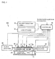
- FIG. 1 illustrates a semiconductor laser 10 in accordance with a first embodiment and a structure of a laser device 100 having the semiconductor laser 10.
- the laser device 100 has the semiconductor laser 10, a temperature control device 20, a wavelength detector 30, an output detector 40 and a controller 50.
- the semiconductor laser 10 is mounted on the temperature control device 20. A description will be given of each part.
- the semiconductor laser 10 has a structure in which a SG-DBR region 11, a SG-DFB region 12 and a semiconductor amplifier (SOA: Semiconductor Optical Amplifier) region 13 are coupled in order.
- the SG-DBR region 11 has an optical waveguide in which gratings are provided at a given interval. That is, the optical waveguide of the SG-DBR region 11 has a first region that has a diffraction grating and a second region that is optically connected to the first region and acts as a spacer.
- the optical waveguide of the SG-DBR region 11 is composed of semiconductor crystalline having an absorption edge wavelength on the shorter-wavelength side compared to a laser oscillation wavelength.
- a heater 14 is provided on the SG-DBR region 11.
- the SG-DFB region 12 has an optical waveguide in which gratings are provided at a given interval. That is, the optical waveguide of the SG-DFB region 12 has a first region that has a grating and a second region that is optically connected to the first region and acts as a spacer.
- the optical waveguide of the SG-DFB region 12 is composed of semiconductor crystal amplifying light of a desired wavelength of a laser oscillation.
- An electrode 15 is provided on the SG-DFB region 12.
- the SOA region 13 is composed of crystalline semiconductor for amplifying light or for absorbing a light with a current control.
- An electrode 16 is provided on the SOA region 13.
- the optical waveguides of the SG-DBR region 11, the SG-DFB region 12 and the SOA region 13 are optically connected to each other.
- the semiconductor laser 10 is mounted on the temperature control device 20.
- a thermistor 21 for detecting the temperature of the temperature control device 20 is provided on the temperature control device 20.
- the wavelength detector 30 has a light-receiving element for detecting the intensity of a lasing light and a light-receiving element for detecting the intensity of a lasing light that passes through an etalon and has a wavelength property.
- the output detector 40 has a light-receiving element for detecting the intensity of lasing light passing through the SOA region 13.
- the wavelength detector 30 is arranged on the side of the SG-DBR region 11, and the output detector 40 is arranged on the side of the SOA region 13.
- the structure of the semiconductor laser 10 is not so limited.
- the detectors may be arranged in reverse.
- the controller 50 has a control portion having a central processing unit (CPU), a random-access memory (RAM), a read-only memory (ROM) and so on and an electrical power supply.
- the ROM of the controller 50 stores control information and a control program for the semiconductor laser 10.
- the control information is, for example, stored in a look-up table 51 and a heater correction table 52.
- FIG. 2 illustrates an example of such a look-up table 51.
- the look-up table 51 includes an initial setting value and a target value for feedback control.
- the initial setting value includes an initial current value I LD of the SG-DFB region 12, an initial current value I SOA of the SOA region 13, an initial current value I Heater of the heater 14 and the initial temperature value T LD of the temperature control device 20.
- the target value for the feedback control includes a target value Im1 for feedback control of the output detector 40 and a target value Im3/Im2 for feedback control of the wavelength detector 30.
- the controller 50 refers to the look-up table 51 and obtains the initial current value I LD , the initial current value I SOA , the initial current value I Heater and the initial temperature value T LD .
- the controller 50 controls the temperature control device 20 so that a temperature is controlled to be the initial temperature value T LD . Also, the temperature of the semiconductor laser 10 is controlled to be constant near the initial temperature value T LD . Consequently the equivalent refractive index of the optical waveguide of the SG-DFB region 12 is controlled to be a given value. Next, the controller 50 provides a current of the initial current value I Heater to the heater 14. Therefore, the equivalent refractive index of the optical waveguide of the SG-DBR region 11 is controlled to be a given value. Next, the controller 50 provides a current of the initial current value I LD to the electrode 15. As a result, light is generated in the optical waveguide of the SG-DFB region 12.
- the light generated in the SG-DFB region 12 is repeatedly reflected and amplified in the optical waveguide of the SG-DBR region 11 and the SG-DFB region 12. This results in a laser oscillation.
- the controller 50 provides a current of the initial current value I SOA to the electrode 16. With the control, the semiconductor laser 10 emits a lasing light at an initial wavelength corresponding to a set channel.
- FIGS. 3A and 3B illustrate the principle of selection of an oscillation wavelength.
- FIG. 3A illustrates a reflection spectrum in the SG-DBR region 11.
- FIG. 3B illustrates a gain spectrum in the SG-DFB region 12.
- the horizontal axis in FIG. 3A and FIG. 3B indicates wavelength.
- the vertical axis of FIG. 3A and FIG. 3B indicates the reflectivity and the intensity of the gain.
- peak wavelength profiles appear periodically at a given wavelength interval in the reflection spectrum of the SG-DBR region 11, and as shown in FIG. 3B , peak wavelength profiles appear periodically at a given wavelength interval in the gain spectrum of the SG-DFB region 12.
- the gain peak intensity gets lower at a wavelength away from a center wavelength.
- the reflection spectrum and the gain spectrum are variable according to the temperature of the temperature control device 20 and the heater 14.
- the wavelength ⁇ 3, one of the peak wavelengths of the SG-DBR region 11 corresponds to the peak wavelength of the SG-DFB region 12. Therefore, the semiconductor laser 10 oscillates at the wavelength ⁇ 3.
- the controller 50 corrects the temperature of the temperature control device 20 so that the detection result ratio Im3/Im2 of two light-receiving elements in the wavelength detector 30 is within a given range including the target value Im3/Im2 for the feedback control obtained from the look-up table 51.
- the present inventors have found that the correction amount of the wavelength property of the SG-DBR region 11 and the SG-DFB region 12 is not always the same.
- FIGS. 4A and 4B illustrate each wavelength property of the SG-DBR region 11 and the SG-DFB region 12 in a case where the temperature of the temperature control device 20 has changed.
- the dashed lines in FIG. 4A and FIG. 4B indicate a reflection spectrum and a gain spectrum in the case where each peak wavelength overlaps at the wavelength ⁇ 3.
- the solid lines of FIG. 4A and FIG. 4B indicate a reflection spectrum and a gain spectrum in the case where the temperature of the temperature control device 20 is changed; in the present example the temperature of the temperature control device 20 is lowered.
- the change in the reflection spectrum of the SG-DBR region 11 is larger than that of the gain spectrum of the SG-DFB region 12.
- the differential between the changing amounts of the wavelength property with respect to the temperature change brought about by the temperature control device 20 is not limited to the case of the combination of the SG-DBR region 11 and the SG-DFB region 12. For example, even if two SG-DBR regions are provided as the wavelength selection portion, the changing amounts of the wavelength property with respect to the temperature changing of the temperature control device 20 are different from each other when the wavelength properties of the SG-DBR regions are different from each other.
- the wavelength property of the two SG-DBR regions responds differently with respect to the same temperature changing even if the two SG-DBR regions are subjected to the same temperature changing, because the wavelength properties of the two SG-DBR regions are different from each other. That is, there is a problem similar to the above-mentioned case when the semiconductor laser has wavelength selection portions having a different wavelength property, because the changing amounts of the wavelength property is different from each other with respect to the temperature changing of the temperature control device.
- the problem gets larger because of a device structure differential of the wavelength selection portions.
- a groove is formed on both sides of a heater in order to improve the controllability of the wavelength selection portion when using the heater, if the heater controls the wavelength selection portion.
- the thermal conductivity from a temperature control device of a wavelength selection portion not having a groove is different from that of the wavelength selection portion having the groove. This results in an enlargement of the differential of the wavelength property.
- the changing amount of the reflection spectrum in the SG-DBR region 11 is more than that of the gain spectrum in the SG-DFB region.
- the relation may be inverted.
- FIG. 5 illustrates an enlarged view of the peak at the wavelength ⁇ 3 of the SG-DBR region 11 and the SG-DFB region 12.
- the right-hand dashed line indicates the peak of the SG-DBR region 11 and the SG-DFB region 12 before correction of the temperature of the temperature control device 20.
- the peak profile of the SG-DBR region 11 is the same as that of the SG-DFB region 12, for convenience.
- the two overlap indicates the peak of the SG-DFB region 12 after the correction of the temperature of the temperature control device 20.
- the thick line indicates the peak of the SG-DBR region 11 after the correction of the temperature of the temperature control device 20.
- the oscillation wavelength is a wavelength (a wavelength ⁇ 3' in FIG. 5 ) having the largest reflection intensity of the wavelengths where the peak of the SG-DBR region 11 overlaps with that of the SG-DFB region 12, as indicated by the second dashed line.
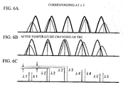
- FIG. 6A and FIG. 6B illustrate the transition of the reflection intensity at wavelengths other than ⁇ 3.
- the reflection intensity differential between the wavelength ⁇ 3' and the wavelength ⁇ 2' after the correction of the temperature is smaller than that between the wavelength ⁇ 3 and the wavelength ⁇ 2 before the correction of the temperature. That is, the oscillation condition at the wavelength ⁇ 3' is closer to that at the wavelength ⁇ 2' after the correction of the temperature.
- the oscillation wavelength may be the unexpected wavelength ⁇ 2' because of the changing of another parameter.
- the oscillation condition can vary drastically because of a slight differential of the wavelength property of the wavelength selection portions, with the wavelength controlling method in which a Vernier effect is obtained, and a desirable oscillation condition is selected when a plurality of the wavelength selection portions having a different wavelength property are combined.
- the controller 50 corrects the differential between the changing amounts of the reflection spectrum of the SG-DBR region 11 and the gain spectrum of the SG-DFB region 12 caused by the temperature control of the temperature control device 20, with the heat value of the heater 14.
- FIG. 7 is a flowchart showing a control method for the semiconductor laser 10.
- the controller 50 refers to the look-up table 51 and obtains the initial current value I LD , the initial current value I SOA , the initial current value I Heater and the initial temperature value T LD (Step S1).
- the controller 50 starts a laser oscillation of the semiconductor laser 10 according to the initial setting value obtained in Step S1 (Step S2).
- the controller 50 determines whether the lasing wavelength is within a required range according to the detection result of the wavelength detector 30 (Step S3). If it is not determined that the lasing wavelength is within the required range, the controller 50 corrects the temperature of the temperature control device 20 (Step S4). In this case, the peak wavelength of the gain spectrum in the optical waveguide of the SG-DFB region 12 changes.
- the controller 50 obtains the detection result of the thermistor 21 (Step S5).
- the controller 50 corrects the temperature of the heater 14 with reference to the heater correction table 52 (Step S6).
- the controller 50 monitors the detection result of the thermistor 21 obtained in Step S6.
- the controller 50 corrects the temperature of the heater 14 when the detection result is changed.
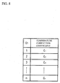
- FIG. 8 illustrates the heater correction table 52.
- the heater correction table 52 includes a temperature correction coefficient C at every channel.
- the temperature correction coefficient C is a coefficient for calculating correction value for the heater 14 with respect to the temperature changing amount of the temperature control device 20. It is possible to obtain a differential between the changing amounts of the wavelength property of the SG-DFB region 12 and the SG-DBR region 11 generated before the temperature transition of the temperature control device 20, in advance.
- the temperature correction coefficient C is prepared in advance. Each temperature correction coefficient C is prepared individually, because there is a case where the temperature correction value differs according to the channels.
- the temperature correction coefficient C is a coefficient for correcting the heat value of the heater according to the temperature differential between before and after the temperature control.
- the temperature correction coefficient C is prepared as a current amount in order to correct the driving current of the heater.
- T LD is the temperature of the thermistor 21 before detecting a temperature change by the controller 50.
- T LD ' is the temperature of the thermistor 21 after detecting temperature changing by the controller 50.
- the calculated ⁇ I Heater is added to the driving current of the heater before detecting the temperature change by the controller 50, and is provided to the heater 14.
- Step S3 the controller 50 executes Step S3 again.
- the lasing wavelength is feedback-controlled to be desirable constant value. If it is determined that the lasing wavelength is within the required range in the Step S3, the controller 50 determines whether the optical intensity of the lasing light is within the required range (Step S7).
- the controller 50 obtains the target value Im1 for feedback control from the look-up table 51, obtains the detection result Im1 from the light-receiving element in the output detector 40, and determines whether the detection result Im1 is within a required range including the target value Im1 for feedback control.
- Step S7 If it is not determined that the optical intensity of the lasing light is within the required range in the Step S7, the controller 50 corrects the current to the electrode 16 (Step S8). After that, the controller 50 executes Step S7 again. With the loop, the optical intensity of the lasing light is feedback-controlled to be a desired constant value. If it is determined that the optical intensity of the lasing light is within the required range in the Step S7, the controller 50 executes Step S3 again.
- the peak of the SG-DBR region 11 and the SG-DFB region 12 may be closer to a condition before the temperature control of the temperature control device 20. Therefore, the semiconductor laser 10 may oscillate at the desired wavelength.
- the temperature correction coefficient C may be obtained in advance by detecting the temperature changing of the SG-DBR region 11 in a case where the temperature of the temperature control device 20 is changed.
- the temperature correction value C may be determined according to each channel or may be common with respect to each channel.
- the heater correction table 52 may include a correction temperature of the heater 14 according to the temperature correction amount of the temperature control device 20.
- the semiconductor laser has an SG-DBR region and an SG-DFB region.
- the structure is not limited to this.
- the present invention may be applied to a semiconductor laser in which an active region acting as a gain region is between a pair of SG-DBR regions.
- a heater is provided on each of the SG-DBR regions or one of the SG-DBR regions. In this case, it is possible to correct each temperature of the heaters with use of the temperature correction coefficient when the temperature of the temperature control device is changed.
- the present invention may be applied to a CSG-DBR (Chirped Sampled Grating Distributed Bragg Reflector).
- CSG-DBR Cold Sampled Grating Distributed Bragg Reflector
- space regions connecting gratings have a different length from each other, being different from the SG-DBR region. Therefore, there is wavelength dependence in a peak intensity of a reflection spectrum of the CSG-DBR region. In this case, the peak intensity of the reflection spectrum is enlarged in a given wavelength range. It is therefore possible to restrain oscillation at wavelengths other than a desired wavelength, if a wavelength in a wavelength range having relatively high intensity is used as a lasing wavelength.
- the temperature of each segment having a grating and a spacer may be controllable with heaters provided separately according to each segment.
- the reflection spectrum of the SG-DBR region is controlled with the use of the heater.
- the reflection spectrum of the SG-DBR region may be controlled with a current injection to the SG-DBR region. In this case, current injection amount may be corrected when the temperature control device 20 controls the temperature of the SG-DBR region.
- the SG-DFB region 12 corresponds to the active region.
- the SG-DBR region 11 corresponds to the optical waveguide.
- the SG-DFB region 12 and the SG-DBR region 11 correspond to the plurality of the wavelength selection portions.
Landscapes
- Physics & Mathematics (AREA)
- Condensed Matter Physics & Semiconductors (AREA)
- General Physics & Mathematics (AREA)
- Electromagnetism (AREA)
- Optics & Photonics (AREA)
- Semiconductor Lasers (AREA)
Claims (12)
- Verfahren zur Steuerung eines Halbleiterlasers, der einen ersten Wellenlängenselektionsteil (11), der eine Heizvorrichtung (14) hat, und einen zweiten Wellenlängenselektionsteil (12) hat, der eine gegenüber dem ersten Wellenlängenselektionsteil verschiedene Wellenlängeneigenschaft hat und an einer Temperatursteuervorrichtung (20) montiert ist, gekennzeichnet dadurch, dass es enthält:einen ersten Schritt des Startens einer Laseroszillation des Halbleiterlasers unter einer Bedingung, dass eine Wellenlängenspitze des ersten Wellenlängenselektionsteils (11) und eine Wellenlängenspitze des zweiten Wellenlängenselektionsteils (12) miteinander bei einer gewünschten Wellenlänge überlappen;einem zweiten Schritt des Korrigierens der Temperatur der Temperatursteuervorrichtung gemäß einem Detektionsergebnis eines Wellenlängendetektors (30), das eine detektierte Ausgangswellenlänge des Halbleiterlasers ist; undeinem dritten Schritt des Steuerns der Heizvorrichtung (14) des ersten Wellenlängenselektionsteils, dadurch gekennzeichnet, dass in dem dritten Schritt die Heizvorrichtung des ersten Wellenlängenselektionsteils in einer solchen Weise gesteuert wird, dass Änderungen bei den Unterschieden zwischen den Wellenlängeneigenschaften des ersten Wellenlängenselektionsteils (11) und des zweiten Wellenlängenselektionsteils (12) verringert werden, wobei die Unterschiede durch Temperaturkorrekturen verursacht werden, die von der Temperatursteuervorrichtung in dem zweiten Schritt hervorgerufen werden.
- Verfahren nach Anspruch 1, wobei der dritte Schritt gemäß einem Temperaturdetektionsergebnis der Temperatursteuervorrichtung ausgeführt wird.
- Verfahren nach Anspruch 1 oder 2, wobei wenigstens eines der Wellenlängenselektionsteile einen optischen Wellenleiter hat, der ein beugendes Gitter hat.
- Verfahren nach Anspruch 3, wobei der optische Wellenleiter eine erste Region, die ein beugendes Gitter hat, und eine zweite Region hat, die mit der ersten Region verbunden ist und als ein Abstandhalter wirkt.
- Verfahren nach einem der vorhergehenden Ansprüche, wobei wenigstens eines der Wellenlängenselektionsteile eine aktive Region ist, die ein beugendes Gitter hat.
- Verfahren nach Anspruch 5, wobei die aktive Region eine erste Region, die ein beugendes Gitter hat, und eine zweite Region hat, die mit der ersten Region verbunden ist und als ein Abstandhalter wirkt.
- Verfahren nach einem der vorhergehenden Ansprüche, wobei die Wellenlängeneigenschaft der Mehrzahl von Wellenlängenselektionsteilen ein Reflexionsspektrum oder ein Verstärkungsspektrum des Wellenlängenselektionsteils ist.
- Verfahren nach Anspruch 7, wobei das Reflexionsspektrum oder das Verstärkungsspektrum periodische Spitzen in gegebenen Intervallen hat.
- Verfahren nach Anspruch 8, wobei die Mehrzahl von Wellenlängenselektionsteilen eine Oszillationswellenlänge unter Verwendung eines Vernier-Effekts selektieren, der durch eine Kombination der Wellenlängeneigenschaft verursacht wird.
- Verfahren nach einem der vorhergehenden Ansprüche, wobei:wenigstens eines der Wellenlängenselektionsteile einen Brechungsindex-Steuerteil hat, der einen äquivalenten Brechungsindex davon steuert; undder Schritt des Verringerns der Änderung des Unterschiedsbetrages der Wellenlängeneigenschaft der Wellenlängenselektionsteile durch Steuern des Brechungsindex-Steuerteils gesteuert wird.
- Verfahren nach Anspruch 10, wobei der Brechungsindex-Steuerteil eine Heizvorrichtung oder ein Stromeinspeisungsteil ist.
- Halbleiterlaservorrichtung (100), enthaltend einen Laser (10), eine Temperatursteuervorrichtung (20) und eine Steuerung (50), dadurch gekennzeichnet, dass die Laservorrichtung ausgelegt ist, um ein Steuerverfahren nach einem der vorhergehenden Ansprüche auszuführen.
Applications Claiming Priority (1)
| Application Number | Priority Date | Filing Date | Title |
|---|---|---|---|
| JP2007189340A JP4943255B2 (ja) | 2007-07-20 | 2007-07-20 | 半導体レーザの制御方法 |
Publications (3)
| Publication Number | Publication Date |
|---|---|
| EP2017928A2 EP2017928A2 (de) | 2009-01-21 |
| EP2017928A3 EP2017928A3 (de) | 2009-09-02 |
| EP2017928B1 true EP2017928B1 (de) | 2016-09-14 |
Family
ID=39934479
Family Applications (1)
| Application Number | Title | Priority Date | Filing Date |
|---|---|---|---|
| EP08160838.2A Ceased EP2017928B1 (de) | 2007-07-20 | 2008-07-21 | Verfahren zur Steuerung eines Halbleiterlasers |
Country Status (4)
| Country | Link |
|---|---|
| US (1) | US7813391B2 (de) |
| EP (1) | EP2017928B1 (de) |
| JP (1) | JP4943255B2 (de) |
| CN (1) | CN101350498B (de) |
Families Citing this family (27)
| Publication number | Priority date | Publication date | Assignee | Title |
|---|---|---|---|---|
| JP2010226032A (ja) * | 2009-03-25 | 2010-10-07 | Sumitomo Electric Device Innovations Inc | 光半導体装置 |
| JP2011142584A (ja) * | 2010-01-08 | 2011-07-21 | Fujitsu Optical Components Ltd | 光伝送装置 |
| JP5457873B2 (ja) * | 2010-02-18 | 2014-04-02 | 住友電工デバイス・イノベーション株式会社 | 波長可変レーザの制御方法 |
| CN103155309B (zh) * | 2010-10-29 | 2016-06-01 | 古河电气工业株式会社 | 光放大装置以及光传送系统 |
| JP2014013823A (ja) * | 2012-07-04 | 2014-01-23 | Sumitomo Electric Ind Ltd | 波長可変半導体レーザの制御方法 |
| CN102723666B (zh) * | 2012-05-03 | 2016-01-20 | 清华大学 | 半导体激光器模块装置及其控制方法 |
| JP6253082B2 (ja) * | 2012-07-31 | 2017-12-27 | 住友電工デバイス・イノベーション株式会社 | 波長可変レーザの制御方法 |
| JP6308456B2 (ja) | 2013-07-31 | 2018-04-11 | 住友電工デバイス・イノベーション株式会社 | 波長可変レーザの制御方法 |
| JP6292499B2 (ja) | 2013-08-30 | 2018-03-14 | 住友電工デバイス・イノベーション株式会社 | 波長可変レーザの制御方法 |
| JP2015050284A (ja) | 2013-08-30 | 2015-03-16 | 住友電工デバイス・イノベーション株式会社 | 波長可変レーザの制御方法 |
| JP6308089B2 (ja) * | 2013-09-30 | 2018-04-11 | 住友電気工業株式会社 | 光半導体装置の制御方法 |
| JP6304582B2 (ja) | 2013-10-30 | 2018-04-04 | 住友電工デバイス・イノベーション株式会社 | 波長可変レーザの制御方法 |
| JP2015088626A (ja) | 2013-10-30 | 2015-05-07 | 住友電気工業株式会社 | 波長可変レーザ装置の試験方法および波長可変レーザ装置 |
| US9231369B2 (en) | 2013-10-31 | 2016-01-05 | Sumitomo Electric Device Innovations, Inc. | Method for controlling wavelength tunable laser |
| JP6319718B2 (ja) | 2013-11-29 | 2018-05-09 | 住友電工デバイス・イノベーション株式会社 | 波長可変レーザの制御方法 |
| JP2015126195A (ja) | 2013-12-27 | 2015-07-06 | 住友電工デバイス・イノベーション株式会社 | 波長可変レーザの制御方法 |
| JP6319721B2 (ja) * | 2014-01-31 | 2018-05-09 | 住友電工デバイス・イノベーション株式会社 | 波長可変レーザの制御方法 |
| JP2015144191A (ja) | 2014-01-31 | 2015-08-06 | 住友電工デバイス・イノベーション株式会社 | 波長可変レーザの波長切り替え方法 |
| US9531155B2 (en) * | 2014-04-09 | 2016-12-27 | Applied Optoelectronics, Inc. | Switched radio frequency (RF) driver for tunable laser with multiple in-line sections |
| JP6821901B2 (ja) * | 2016-07-11 | 2021-01-27 | 住友電工デバイス・イノベーション株式会社 | 波長可変レーザの駆動条件設定方法及び波長可変レーザシステム |
| US20210108127A1 (en) * | 2017-03-28 | 2021-04-15 | Cargill, Incorporated | Beta-glucan compositions and shearing to provide viscosity maintenance thereof |
| US11764542B2 (en) | 2017-12-15 | 2023-09-19 | Horiba, Ltd. | Semiconductor laser device, and method and program for driving the same |
| JP7088609B2 (ja) * | 2018-06-27 | 2022-06-21 | 住友電工デバイス・イノベーション株式会社 | 波長可変レーザ装置の制御方法 |
| JP7259562B2 (ja) | 2018-07-19 | 2023-04-18 | 住友電気工業株式会社 | 波長可変光源及びその波長制御方法 |
| CN110888245B (zh) * | 2018-09-10 | 2023-09-22 | 苏州旭创科技有限公司 | 可调谐激光器的波长选择方法及波长选择装置 |
| CN113424381B (zh) * | 2019-02-14 | 2024-03-08 | 古河电气工业株式会社 | 波长可变光源装置以及波长可变激光元件的控制方法 |
| JP7516059B2 (ja) * | 2020-02-12 | 2024-07-16 | 古河電気工業株式会社 | レーザ装置およびその制御方法 |
Family Cites Families (6)
| Publication number | Priority date | Publication date | Assignee | Title |
|---|---|---|---|---|
| JP2914248B2 (ja) | 1995-09-23 | 1999-06-28 | 日本電気株式会社 | 波長可変半導体レーザ素子 |
| US6788719B2 (en) * | 2000-05-04 | 2004-09-07 | Agility Communications, Inc. | Open loop control of SGDBR lasers |
| JP5148815B2 (ja) * | 2005-01-20 | 2013-02-20 | 住友電気工業株式会社 | 光送信モジュール |
| JP4657853B2 (ja) * | 2005-08-11 | 2011-03-23 | 住友電工デバイス・イノベーション株式会社 | 半導体レーザ、レーザモジュール、光学部品、レーザ装置、半導体レーザの製造方法および半導体レーザの制御方法 |
| CN100521416C (zh) | 2005-12-27 | 2009-07-29 | 优迪那半导体有限公司 | 激光装置、激光模块、半导体激光器及其制造方法 |
| JP4629022B2 (ja) * | 2005-12-27 | 2011-02-09 | 住友電工デバイス・イノベーション株式会社 | レーザ装置、レーザモジュール、および、半導体レーザ |
-
2007
- 2007-07-20 JP JP2007189340A patent/JP4943255B2/ja not_active Expired - Fee Related
-
2008
- 2008-07-18 US US12/175,872 patent/US7813391B2/en active Active
- 2008-07-18 CN CN2008101339614A patent/CN101350498B/zh active Active
- 2008-07-21 EP EP08160838.2A patent/EP2017928B1/de not_active Ceased
Also Published As
| Publication number | Publication date |
|---|---|
| US7813391B2 (en) | 2010-10-12 |
| CN101350498B (zh) | 2011-05-11 |
| US20090022186A1 (en) | 2009-01-22 |
| JP2009026996A (ja) | 2009-02-05 |
| EP2017928A3 (de) | 2009-09-02 |
| CN101350498A (zh) | 2009-01-21 |
| JP4943255B2 (ja) | 2012-05-30 |
| EP2017928A2 (de) | 2009-01-21 |
Similar Documents
| Publication | Publication Date | Title |
|---|---|---|
| EP2017928B1 (de) | Verfahren zur Steuerung eines Halbleiterlasers | |
| EP2017927B1 (de) | Verfahren zur Steuerung eines Halbleiterlasers | |
| US9413138B2 (en) | Method of controlling wavelength tunable laser, control data structure of wavelength tunable laser, and wavelength tunable laser | |
| US7929581B2 (en) | Testing method of wavelength-tunable laser, controlling method of wavelength-tunable laser and laser device | |
| JP5154581B2 (ja) | レーザ装置およびレーザ装置の制御データ | |
| EP2915227B1 (de) | Dbr-halbleiterlaser | |
| EP2017666A1 (de) | Thermooptische Vorrichtung und Steuerungsverfahren | |
| US9450378B2 (en) | Method for controlling wavelength-tunable laser | |
| JP6951983B2 (ja) | 波長可変レーザ装置、及び波長可変レーザ装置の波長制御方法 | |
| JP2009044024A (ja) | 半導体レーザ装置、および半導体レーザの制御方法 | |
| US8279907B2 (en) | Semiconductor laser device and method for controlling semiconductor laser | |
| CN101350496B (zh) | 光器件及其控制方法 | |
| US20150063383A1 (en) | Method for controlling tunable wavelength laser | |
| US9444220B2 (en) | Method for controlling wavelength tunable laser | |
| US8681826B2 (en) | Method for tuning semiconductor laser | |
| JP6256745B2 (ja) | 波長可変レーザの制御方法 | |
| JP2015088676A (ja) | 波長可変レーザの制御方法 | |
| JP2024114192A (ja) | 波長可変レーザ装置、及び波長可変レーザ装置の波長制御方法 | |
| JP2015088677A (ja) | 波長可変レーザの制御方法 |
Legal Events
| Date | Code | Title | Description |
|---|---|---|---|
| PUAI | Public reference made under article 153(3) epc to a published international application that has entered the european phase |
Free format text: ORIGINAL CODE: 0009012 |
|
| AK | Designated contracting states |
Kind code of ref document: A2 Designated state(s): AT BE BG CH CY CZ DE DK EE ES FI FR GB GR HR HU IE IS IT LI LT LU LV MC MT NL NO PL PT RO SE SI SK TR |
|
| AX | Request for extension of the european patent |
Extension state: AL BA MK RS |
|
| PUAL | Search report despatched |
Free format text: ORIGINAL CODE: 0009013 |
|
| AK | Designated contracting states |
Kind code of ref document: A3 Designated state(s): AT BE BG CH CY CZ DE DK EE ES FI FR GB GR HR HU IE IS IT LI LT LU LV MC MT NL NO PL PT RO SE SI SK TR |
|
| AX | Request for extension of the european patent |
Extension state: AL BA MK RS |
|
| RIC1 | Information provided on ipc code assigned before grant |
Ipc: H01S 5/125 20060101ALI20090724BHEP Ipc: H01S 5/0625 20060101ALI20090724BHEP Ipc: H01S 5/06 20060101AFI20081113BHEP Ipc: H01S 5/12 20060101ALN20090724BHEP |
|
| 17P | Request for examination filed |
Effective date: 20100224 |
|
| AKX | Designation fees paid |
Designated state(s): DE FR GB |
|
| 17Q | First examination report despatched |
Effective date: 20141006 |
|
| GRAP | Despatch of communication of intention to grant a patent |
Free format text: ORIGINAL CODE: EPIDOSNIGR1 |
|
| INTG | Intention to grant announced |
Effective date: 20160314 |
|
| GRAS | Grant fee paid |
Free format text: ORIGINAL CODE: EPIDOSNIGR3 |
|
| GRAA | (expected) grant |
Free format text: ORIGINAL CODE: 0009210 |
|
| RAP1 | Party data changed (applicant data changed or rights of an application transferred) |
Owner name: SUMITOMO ELECTRIC DEVICE INNOVATIONS, INC. |
|
| AK | Designated contracting states |
Kind code of ref document: B1 Designated state(s): DE FR GB |
|
| REG | Reference to a national code |
Ref country code: GB Ref legal event code: FG4D |
|
| REG | Reference to a national code |
Ref country code: DE Ref legal event code: R096 Ref document number: 602008046257 Country of ref document: DE |
|
| REG | Reference to a national code |
Ref country code: FR Ref legal event code: PLFP Year of fee payment: 10 |
|
| REG | Reference to a national code |
Ref country code: DE Ref legal event code: R097 Ref document number: 602008046257 Country of ref document: DE |
|
| PLBE | No opposition filed within time limit |
Free format text: ORIGINAL CODE: 0009261 |
|
| STAA | Information on the status of an ep patent application or granted ep patent |
Free format text: STATUS: NO OPPOSITION FILED WITHIN TIME LIMIT |
|
| 26N | No opposition filed |
Effective date: 20170615 |
|
| REG | Reference to a national code |
Ref country code: FR Ref legal event code: PLFP Year of fee payment: 11 |
|
| P01 | Opt-out of the competence of the unified patent court (upc) registered |
Effective date: 20230515 |
|
| PGFP | Annual fee paid to national office [announced via postgrant information from national office to epo] |
Ref country code: GB Payment date: 20240530 Year of fee payment: 17 |
|
| PGFP | Annual fee paid to national office [announced via postgrant information from national office to epo] |
Ref country code: FR Payment date: 20240611 Year of fee payment: 17 |
|
| PGFP | Annual fee paid to national office [announced via postgrant information from national office to epo] |
Ref country code: DE Payment date: 20240529 Year of fee payment: 17 |
|
| REG | Reference to a national code |
Ref country code: DE Ref legal event code: R119 Ref document number: 602008046257 Country of ref document: DE |
|
| GBPC | Gb: european patent ceased through non-payment of renewal fee |
Effective date: 20250721 |
|
| PG25 | Lapsed in a contracting state [announced via postgrant information from national office to epo] |
Ref country code: GB Free format text: LAPSE BECAUSE OF NON-PAYMENT OF DUE FEES Effective date: 20250721 |
|
| PG25 | Lapsed in a contracting state [announced via postgrant information from national office to epo] |
Ref country code: DE Free format text: LAPSE BECAUSE OF NON-PAYMENT OF DUE FEES Effective date: 20260203 |
|
| PG25 | Lapsed in a contracting state [announced via postgrant information from national office to epo] |
Ref country code: FR Free format text: LAPSE BECAUSE OF NON-PAYMENT OF DUE FEES Effective date: 20250731 |