EP2019436A2 - Détecteur de radiation ultra haute résolution (UHRD) et son procédé de fabrication - Google Patents
Détecteur de radiation ultra haute résolution (UHRD) et son procédé de fabrication Download PDFInfo
- Publication number
- EP2019436A2 EP2019436A2 EP08102994A EP08102994A EP2019436A2 EP 2019436 A2 EP2019436 A2 EP 2019436A2 EP 08102994 A EP08102994 A EP 08102994A EP 08102994 A EP08102994 A EP 08102994A EP 2019436 A2 EP2019436 A2 EP 2019436A2
- Authority
- EP
- European Patent Office
- Prior art keywords
- anode
- detector
- region
- type
- circularity
- Prior art date
- Legal status (The legal status is an assumption and is not a legal conclusion. Google has not performed a legal analysis and makes no representation as to the accuracy of the status listed.)
- Withdrawn
Links
Images

Classifications
-
- H—ELECTRICITY
- H10—SEMICONDUCTOR DEVICES; ELECTRIC SOLID-STATE DEVICES NOT OTHERWISE PROVIDED FOR
- H10F—INORGANIC SEMICONDUCTOR DEVICES SENSITIVE TO INFRARED RADIATION, LIGHT, ELECTROMAGNETIC RADIATION OF SHORTER WAVELENGTH OR CORPUSCULAR RADIATION
- H10F30/00—Individual radiation-sensitive semiconductor devices in which radiation controls the flow of current through the devices, e.g. photodetectors
- H10F30/20—Individual radiation-sensitive semiconductor devices in which radiation controls the flow of current through the devices, e.g. photodetectors the devices having potential barriers, e.g. phototransistors
- H10F30/29—Individual radiation-sensitive semiconductor devices in which radiation controls the flow of current through the devices, e.g. photodetectors the devices having potential barriers, e.g. phototransistors the devices being sensitive to radiation having very short wavelengths, e.g. X-rays, gamma-rays or corpuscular radiation
-
- H—ELECTRICITY
- H10—SEMICONDUCTOR DEVICES; ELECTRIC SOLID-STATE DEVICES NOT OTHERWISE PROVIDED FOR
- H10F—INORGANIC SEMICONDUCTOR DEVICES SENSITIVE TO INFRARED RADIATION, LIGHT, ELECTROMAGNETIC RADIATION OF SHORTER WAVELENGTH OR CORPUSCULAR RADIATION
- H10F71/00—Manufacture or treatment of devices covered by this subclass
-
- H—ELECTRICITY
- H10—SEMICONDUCTOR DEVICES; ELECTRIC SOLID-STATE DEVICES NOT OTHERWISE PROVIDED FOR
- H10F—INORGANIC SEMICONDUCTOR DEVICES SENSITIVE TO INFRARED RADIATION, LIGHT, ELECTROMAGNETIC RADIATION OF SHORTER WAVELENGTH OR CORPUSCULAR RADIATION
- H10F77/00—Constructional details of devices covered by this subclass
- H10F77/10—Semiconductor bodies
- H10F77/14—Shape of semiconductor bodies; Shapes, relative sizes or dispositions of semiconductor regions within semiconductor bodies
- H10F77/147—Shapes of bodies
-
- Y—GENERAL TAGGING OF NEW TECHNOLOGICAL DEVELOPMENTS; GENERAL TAGGING OF CROSS-SECTIONAL TECHNOLOGIES SPANNING OVER SEVERAL SECTIONS OF THE IPC; TECHNICAL SUBJECTS COVERED BY FORMER USPC CROSS-REFERENCE ART COLLECTIONS [XRACs] AND DIGESTS
- Y02—TECHNOLOGIES OR APPLICATIONS FOR MITIGATION OR ADAPTATION AGAINST CLIMATE CHANGE
- Y02E—REDUCTION OF GREENHOUSE GAS [GHG] EMISSIONS, RELATED TO ENERGY GENERATION, TRANSMISSION OR DISTRIBUTION
- Y02E10/00—Energy generation through renewable energy sources
- Y02E10/50—Photovoltaic [PV] energy
Definitions
- the invention concerns generally the technology of a radiation detector in the field of X-ray Fluorescence Spectrometer (XRF), Especially the invention concerns an ultra high-resolution radiation detector (UHRD)and method for fabrication thereof.
- XRF X-ray Fluorescence Spectrometer
- UHRD ultra high-resolution radiation detector
- An energy dispersive X-ray fluorescence (EDXRF) spectrometer makes use of the fact that the pulse height of the detector signal is proportional to the X-ray photon energy, which is correlated with the wavelength. Therefore the optical path is simpler than for WDXRF spectrometers because no crystals or goniometry are needed and the fluorescence photons from the sample hit the detector directly.
- the samples are normally irradiated by X-rays from a tube with lower power than that used with the WDXRF spectrometers.
- the elements and their concentration are identified by counting the pulses at the different energy levels.
- a semiconductor detector is the best choice for the EDXRF spectrometer with great capability.
- Ionizing radiation produces free electrons and holes.
- the number of electron-hole pairs is proportional to the energy transmitted by the radiation to the semiconductor.
- the electron-hole pairs generate an output charge pulse, whose magnitude of which is proportional to the energy of the x-ray photon, Enlarge the evacuation after the amplifier (usually to take above 1000) to the multi-channel pulse analyzer, Count the pulse number separately according to the pulse amplitude, thus obtain the count rates along with the photon energy change distribution curve, namely X energy of light spectrogram.
- Such radiation detectors preferably silicon-based, are commercially available as pn-diodes, silicon strip detectors (SSDs) silicon drift detectors (SDDs), charge coupled devices (CCDs), pixel detectors, etc.
- a traditional solid-state detector type to be used for X-ray detection is the PIN detector.
- the detecting element is a reverse biased PIN diode, one electrode of which is coupled to the gate of a FET (field-effect transistor).
- FET field-effect transistor
- X-ray photons that hit the PIN diode cause a photoelectric effect, creating a number of free electrons and holes in a depleted region formed in the semiconductor material.
- the bias voltage across the PIN diode causes the mobile charge carriers to be drawn to the electrodes, which changes electrode potential.
- An integrator coupled to the FET transforms the change of the PIN diode's electrode potential into a corresponding change in a voltage across a feedback capacitor.
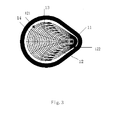
- a drift detector of which is illustrated in FIG. 1 comprises, for example, X-ray photons(1), a semiconductor substrate made of weakly n-doped silicon which has a strongly n-doped(2), centrally located anode(105) on one surface (top side), and has a reverse contact made of a strongly p-doped semiconductor material on the opposite surface (bottom side).
- Annular semiconductor electrodes (101) made of a strongly p-doped semiconductor material in the effective region of the electrodes this results in total depletion of the semiconductor substrate, and also produces an electrical drift field in the semiconductor substrate.
- Radiation interactions cause free electrons to be generated in the semiconductor substrate which are driven through the path (4) to the anode, so that the electrical signal at the anode is a measure of the energy of the radiation. Radiation interactions also cause holes to be generated in the semiconductor substrate which are driven through the path (3).electron/hole pairs are generated therein by known ways and means, the quantity of which is proportional to the intensity or energy of the absorbed radiation. These are separated by the electric field and drift to the main surfaces where with the aid of suitable electrical amplification (9) they can be used for detecting and analyzing the radiation.
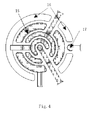
- An SDD (See USA Patent Publication 101,193,216 , Method and circuit arrangement for compensating for rate dependent change of conversion factor in a drift-type radiation detector and a detector appliance), a partially cut-out example of which is illustrated in FIG.2 , differs from a conventional silicon-based PIN diode detector in that it has a field electrode arrangement comprising the so-called drift rings 101 and an amplifier integrated with the diode component.
- the amplifier is most typically a FET (Field-Effect Transistor), the source, gate and drain electrodes appear in FIG. 1 as 102, 103 and 104 respectively.
- the anode and cathode of the detector diode are illustrated as 10105 and 106 respectively in FIG. 2 .
- the FET is integrated with the detector's anode (105).
- the FET is directly coupled to the detector's anode using bump bonding techniques.
- the detector's anode preferably is directly bonded to the FET gate.
- Other FET terminals (drain, source, and resetting electrode) have corresponding bonding pads on the detector structure placed over an insulating layer.
- This level field effect tube uses ion implantation and carries on the heat treatment under the quite low temperature to make.
- the field effect tube channel is manufactures with in-depth phosphorus injection method.
- a pre-amplifier feedback capacitor is coupled directly with the detector structure in a similar way.
- the resetting electrode is used to inject charges into the FET in order to reset it.
- the Semiconductor radiation detector typically have a small anode (105)
- the total input capacitance including the detector, input transistor, and parasitic capacitance due to interconnections and support structures
- the anode with small area offer low leakage current. Because the FET is directly inputted to the detector's anode, and the pre-amplifier feedback capacitor also be built directly into the detector structure in a similar way, which could reduce electronic noise.
- the conventional SDD-based detector has several disadvantages.
- a problem of appliances is the resolution and the peak to background ratio. Since the field effect transistor is integrated onto the center of the semiconductor substrate, the electric field under the FET will twist, which would lead to erroneous figure of the X ray spectrum by undesired signal charge damages. Though the FET occupied a small region of the detector's area, the damage in the sensitive region of the semiconductor substrate upon bonding may cause the detector to fail at high resolution and peak to background ratio.
- the p+ cathodes are fabricated as concentric annular drift rings, Radiation interactions cause signal charges to be generated in the semiconductor substrate which are driven through the annular drift field from all directions to the center, where is the position of the anode. As a result, the drift movement may reduce the input capacitance of the detector.
- the resetting electrode is used to inject charges into the FET in order to reset it by release the leakage current of the FET.
- the leakage current increases, induces a drift of the X ray spectrum and results in low resolution which falsify the signals.
- An objective of the present invention is to provide an improved structure of the semiconductor electrodes for a semiconductor detector with better sensitivity, higher energy resolution and lower electronic noise that can operate at or near room temperature.
- the objectives of the invention are achieved by designing a new shape of p-type drift electrode rings as a function of eliminating the damage in the depletion (effective) region of the semiconductor substrate.
- An ultra high-resolution radiation detector has a detector chip, which is made of n-type semiconductor material, comprising the so-called drift rings and an amplifier integrated with the diode component,
- the amplifier is typically a FET (Field-Effect Transistor), centrally located n-type anode(16) on one surface (top side), the depletion (effective) region ,characterized by the following features:
- an ultra high-resolution radiation detector has a detector chip, which is made of n-type semiconductor material, comprising the so-called drift rings and an amplifier integrated with the diode component,
- the amplifier is typically a FET (11) (Field-Effect Transistor), centrally located n-type anode(16) on one surface (top side), the depletion (effective) region ,characterized by the following features:
- a reset terminal (1101) locate at the centrally anode (16), wherein the reset terminal (1101) is connected with a periodic pulse reset device.
- Said periodic pulse reset device is a device which could periodically providing a line frequency of 10500 hertz or 1000 hertz, pulse width is 200-300 ns, Lead the cumulate charges of the detector discharge rapidly, and then the electrode could be reset without influence from the change of count rate.
- the entrance radiation only can produce electron-hole pairs outer the region encircled by the outermost p-type drift electrode ring (14).
Landscapes
- Measurement Of Radiation (AREA)
- Light Receiving Elements (AREA)
Applications Claiming Priority (1)
| Application Number | Priority Date | Filing Date | Title |
|---|---|---|---|
| CN2007100753345A CN101281148B (zh) | 2007-07-27 | 2007-07-27 | 一种高分辨率的半导体核辐射探测器 |
Publications (2)
| Publication Number | Publication Date |
|---|---|
| EP2019436A2 true EP2019436A2 (fr) | 2009-01-28 |
| EP2019436A3 EP2019436A3 (fr) | 2011-05-04 |
Family
ID=39884950
Family Applications (1)
| Application Number | Title | Priority Date | Filing Date |
|---|---|---|---|
| EP08102994A Withdrawn EP2019436A3 (fr) | 2007-07-27 | 2008-03-27 | Détecteur de radiation ultra haute résolution (UHRD) et son procédé de fabrication |
Country Status (3)
| Country | Link |
|---|---|
| US (1) | US20090026569A1 (fr) |
| EP (1) | EP2019436A3 (fr) |
| CN (1) | CN101281148B (fr) |
Cited By (2)
| Publication number | Priority date | Publication date | Assignee | Title |
|---|---|---|---|---|
| WO2016091993A1 (fr) * | 2014-12-11 | 2016-06-16 | Pnsensor Gmbh | Détecteur de dérive à semi-conducteurs permettant de détecter un rayonnement |
| CN114823964A (zh) * | 2022-05-10 | 2022-07-29 | 湖南脉探芯半导体科技有限公司 | 扇形硅漂移探测器及其制备方法 |
Families Citing this family (18)
| Publication number | Priority date | Publication date | Assignee | Title |
|---|---|---|---|---|
| JP5818238B2 (ja) * | 2010-10-06 | 2015-11-18 | ラピスセミコンダクタ株式会社 | 半導体装置 |
| CN102097521B (zh) * | 2010-10-22 | 2013-03-06 | 北京大学 | 曲面结构的硅漂移探测器 |
| EP2544025A1 (fr) * | 2011-07-07 | 2013-01-09 | FEI Company | Détecteur au silicium à diffusion pour une utilisation dans un appareil de particules chargées |
| US9530902B2 (en) * | 2012-06-20 | 2016-12-27 | Oxford Instruments Analytical Oy | Two-dimensional guard structure and a radiation detector with the same |
| US9008272B2 (en) | 2012-07-18 | 2015-04-14 | Uchicago Argonne, Llc | Precision mechanical structure of an ultra-high-resolution spectrometer for inelastic X-ray scattering instrument |
| CN105676264A (zh) * | 2013-04-26 | 2016-06-15 | 清华大学 | 一种半导体探测器 |
| CN111211197A (zh) * | 2013-12-27 | 2020-05-29 | 同方威视技术股份有限公司 | 高纯锗探测器 |
| CN105700003B (zh) * | 2015-05-21 | 2019-12-13 | 成都理工大学 | 一种半导体制冷的X射线硅pin探测器 |
| ITUB20159390A1 (it) * | 2015-12-24 | 2017-06-24 | Fond Bruno Kessler | Rivelatore a semiconduttore, rivelatore di radiazione e apparecchiatura di rivelazione di radiazione. |
| CN107677723B (zh) * | 2017-09-25 | 2023-06-30 | 付德君 | 一种气体团簇离子束质谱的测量方法和装置 |
| CN111373287B (zh) * | 2017-12-15 | 2025-01-14 | 株式会社堀场制作所 | 放射线检测器和放射线检测装置 |
| WO2020008531A1 (fr) * | 2018-07-03 | 2020-01-09 | オリンパス株式会社 | Détecteur par rayons x |
| CN109873049B (zh) * | 2019-04-01 | 2024-01-05 | 湖南正芯微电子探测器有限公司 | 双面阴极螺旋环渐变式硅漂移探测器及其制备方法 |
| CN110729382B (zh) * | 2019-11-01 | 2024-11-22 | 湘潭大学 | 一种同心环型大面积硅漂移探测器、设计方法及应用 |
| CN113391339B (zh) * | 2021-07-13 | 2024-01-12 | 陕西迪泰克新材料有限公司 | 一种辐射剂量监测装置及其监测方法和制备方法 |
| EP4134709A1 (fr) * | 2021-08-13 | 2023-02-15 | Bruker Nano GmbH | Détecteur de dérive de silicium hybride intégré et son procédé de fabrication |
| CN115826031A (zh) * | 2022-11-16 | 2023-03-21 | 中国科学院上海高等研究院 | 一种高纯锗漂移探测器 |
| CN119828207B (zh) * | 2025-03-20 | 2025-05-23 | 南京大学 | 一种半导体漂移室探测器漂移特性的测试系统及方法 |
Family Cites Families (18)
| Publication number | Priority date | Publication date | Assignee | Title |
|---|---|---|---|---|
| US4688067A (en) * | 1984-02-24 | 1987-08-18 | The United States Of America As Represented By The Department Of Energy | Carrier transport and collection in fully depleted semiconductors by a combined action of the space charge field and the field due to electrode voltages |
| NL8900343A (nl) * | 1989-02-13 | 1990-09-03 | Univ Delft Tech | Plaatsgevoelige stralingsdetector. |
| DE4120443B4 (de) * | 1991-05-07 | 2007-03-22 | Kemmer, Josef, Dr. | Halbleiterdetektor |
| DE4331391A1 (de) * | 1993-09-15 | 1995-03-16 | Josef Dr Kemmer | Halbleiter(detektor)struktur |
| US5677539A (en) * | 1995-10-13 | 1997-10-14 | Digirad | Semiconductor radiation detector with enhanced charge collection |
| DE19620081A1 (de) * | 1996-05-20 | 1997-11-27 | Kemmer Josef Dr | Streifendetektor |
| JP3883678B2 (ja) * | 1997-12-22 | 2007-02-21 | 理学電機工業株式会社 | 半導体装置 |
| WO2000028351A1 (fr) * | 1998-11-09 | 2000-05-18 | Iwanczyk Jan S | Detecteur de rayons gamma utilisant des scintillateurs couples a des photodetecteurs a derive a semi-conducteur |
| US6455858B1 (en) * | 2000-08-13 | 2002-09-24 | Photon Imaging, Inc. | Semiconductor radiation detector |
| US6541836B2 (en) * | 2001-02-21 | 2003-04-01 | Photon Imaging, Inc. | Semiconductor radiation detector with internal gain |
| DE10213812B4 (de) * | 2002-03-27 | 2007-03-29 | MAX-PLANCK-Gesellschaft zur Förderung der Wissenschaften e.V. | Leitungsüberführung für einen Halbleiter-Detektor |
| US7193216B2 (en) * | 2004-10-22 | 2007-03-20 | Oxford Instruments Analytical Oy | Method and circuit arrangement for compensating for rate dependent change of conversion factor in a drift-type radiation detector and a detector appliance |
| US20070072332A1 (en) * | 2005-09-26 | 2007-03-29 | Josef Kemmer | Semiconductor radiation detectors and method for fabrication thereof |
| EP1873834B1 (fr) * | 2006-06-29 | 2008-12-10 | Max-Planck-Gesellschaft zur Förderung der Wissenschaften e.V. | Barrière de remise à zéro, en particulier pour un détecteur à semiconducteur et méthode d'opération correspondante |
| US7339175B1 (en) * | 2006-07-28 | 2008-03-04 | Thermo Electron Scientific Instruments Llc | Feedback circuit for output control in a semiconductor X-ray detector |
| US7858946B2 (en) * | 2007-01-18 | 2010-12-28 | Bruker Ax Microanalysis Gmbh | Energy dispersive X-ray I-FET SDD detector appliance and a method for pulsed reset neutralization of accumulated charges within an energy dispersive X-ray I-FET SDD detector appliance |
| US8932894B2 (en) * | 2007-10-09 | 2015-01-13 | The United States of America, as represented by the Secratary of the Navy | Methods and systems of curved radiation detector fabrication |
| JP5606723B2 (ja) * | 2008-12-25 | 2014-10-15 | 日本電子株式会社 | シリコンドリフト型x線検出器 |
-
2007
- 2007-07-27 CN CN2007100753345A patent/CN101281148B/zh active Active
- 2007-12-07 US US11/999,886 patent/US20090026569A1/en not_active Abandoned
-
2008
- 2008-03-27 EP EP08102994A patent/EP2019436A3/fr not_active Withdrawn
Cited By (2)
| Publication number | Priority date | Publication date | Assignee | Title |
|---|---|---|---|---|
| WO2016091993A1 (fr) * | 2014-12-11 | 2016-06-16 | Pnsensor Gmbh | Détecteur de dérive à semi-conducteurs permettant de détecter un rayonnement |
| CN114823964A (zh) * | 2022-05-10 | 2022-07-29 | 湖南脉探芯半导体科技有限公司 | 扇形硅漂移探测器及其制备方法 |
Also Published As
| Publication number | Publication date |
|---|---|
| US20090026569A1 (en) | 2009-01-29 |
| CN101281148B (zh) | 2011-01-05 |
| EP2019436A3 (fr) | 2011-05-04 |
| CN101281148A (zh) | 2008-10-08 |
Similar Documents
| Publication | Publication Date | Title |
|---|---|---|
| EP2019436A2 (fr) | Détecteur de radiation ultra haute résolution (UHRD) et son procédé de fabrication | |
| Strüder et al. | High-resolution X-ray spectroscopy close to room temperature | |
| JP5523317B2 (ja) | アバランシェフォトダイオード及びアバランシェ照射検出器 | |
| US6455858B1 (en) | Semiconductor radiation detector | |
| KR101143346B1 (ko) | 변형 내부 게이트 구조를 갖는 반도체 방사선 검출기 | |
| US9142702B2 (en) | Semiconductor drift detector and corresponding operating method | |
| JP2014241543A (ja) | 光検出装置およびct装置 | |
| KR102493191B1 (ko) | X-선 센서, x-선 검출기 시스템 및 x-선 영상화 시스템 | |
| US9733365B2 (en) | Gamma ray detector and method of detecting gamma rays | |
| Fiorini et al. | Silicon drift detectors for readout of scintillators in gamma-ray spectroscopy | |
| KR20080085155A (ko) | 가시광 검출용으로 최적화된 반도체 방사선 검출기 | |
| US7518203B2 (en) | Semiconductor structure, particularly in a semiconductor detector, and associated operating method | |
| EP3971997B1 (fr) | Détecteur d'avalanche à faible gain de particules à faible pouvoir pénétrant | |
| US20220085222A1 (en) | Selenium photomultiplier and method for fabrication thereof | |
| Strueder et al. | Room-temperature X-and gamma-ray spectroscopy with silicon drift detectors | |
| Zhang et al. | Development of DEPFET Macropixel detectors | |
| Strüder et al. | High-resolution high-count-rate X-ray spectroscopy with state-of-the-art silicon detectors | |
| WO2002023554A2 (fr) | Detecteur a coordonnees pour particules relativistes | |
| Zha et al. | The analysis of X-ray response of CdZnTe detectors | |
| JP2006261274A (ja) | 半導体検出器および半導体検出器製造方法 | |
| RU2316848C1 (ru) | Микроканальный лавинный фотодиод | |
| Safavi-Naeini et al. | Evaluation of silicon detectors with integrated JFET for biomedical applications | |
| US20250306221A1 (en) | Semiconductor detector | |
| RU2212733C1 (ru) | Полупроводниковый микроканальный детектор с внутренним усилением сигнала | |
| EP4324032A1 (fr) | Capteur de rayonnement à diode |
Legal Events
| Date | Code | Title | Description |
|---|---|---|---|
| PUAI | Public reference made under article 153(3) epc to a published international application that has entered the european phase |
Free format text: ORIGINAL CODE: 0009012 |
|
| AK | Designated contracting states |
Kind code of ref document: A2 Designated state(s): AT BE BG CH CY CZ DE DK EE ES FI FR GB GR HR HU IE IS IT LI LT LU LV MC MT NL NO PL PT RO SE SI SK TR |
|
| AX | Request for extension of the european patent |
Extension state: AL BA MK RS |
|
| PUAL | Search report despatched |
Free format text: ORIGINAL CODE: 0009013 |
|
| AK | Designated contracting states |
Kind code of ref document: A3 Designated state(s): AT BE BG CH CY CZ DE DK EE ES FI FR GB GR HR HU IE IS IT LI LT LU LV MC MT NL NO PL PT RO SE SI SK TR |
|
| AX | Request for extension of the european patent |
Extension state: AL BA MK RS |
|
| AKY | No designation fees paid | ||
| REG | Reference to a national code |
Ref country code: DE Ref legal event code: R108 |
|
| REG | Reference to a national code |
Ref country code: DE Ref legal event code: R108 Effective date: 20120111 |
|
| STAA | Information on the status of an ep patent application or granted ep patent |
Free format text: STATUS: THE APPLICATION IS DEEMED TO BE WITHDRAWN |
|
| 18D | Application deemed to be withdrawn |
Effective date: 20111001 |