WO2020008531A1 - Détecteur par rayons x - Google Patents
Détecteur par rayons x Download PDFInfo
- Publication number
- WO2020008531A1 WO2020008531A1 PCT/JP2018/025235 JP2018025235W WO2020008531A1 WO 2020008531 A1 WO2020008531 A1 WO 2020008531A1 JP 2018025235 W JP2018025235 W JP 2018025235W WO 2020008531 A1 WO2020008531 A1 WO 2020008531A1
- Authority
- WO
- WIPO (PCT)
- Prior art keywords
- electrode
- ray detector
- semiconductor substrate
- region
- distance
- Prior art date
- Legal status (The legal status is an assumption and is not a legal conclusion. Google has not performed a legal analysis and makes no representation as to the accuracy of the status listed.)
- Ceased
Links
Images


Classifications
-
- G—PHYSICS
- G01—MEASURING; TESTING
- G01T—MEASUREMENT OF NUCLEAR OR X-RADIATION
- G01T1/00—Measuring X-radiation, gamma radiation, corpuscular radiation, or cosmic radiation
- G01T1/16—Measuring radiation intensity
- G01T1/24—Measuring radiation intensity with semiconductor detectors
-
- H—ELECTRICITY
- H10—SEMICONDUCTOR DEVICES; ELECTRIC SOLID-STATE DEVICES NOT OTHERWISE PROVIDED FOR
- H10F—INORGANIC SEMICONDUCTOR DEVICES SENSITIVE TO INFRARED RADIATION, LIGHT, ELECTROMAGNETIC RADIATION OF SHORTER WAVELENGTH OR CORPUSCULAR RADIATION
- H10F30/00—Individual radiation-sensitive semiconductor devices in which radiation controls the flow of current through the devices, e.g. photodetectors
- H10F30/20—Individual radiation-sensitive semiconductor devices in which radiation controls the flow of current through the devices, e.g. photodetectors the devices having potential barriers, e.g. phototransistors
Definitions
- the present invention relates to an X-ray detector.
- This phenomenon can be applied to the estimation of the type and amount of a substance such as metal contained in an object.
- an object is irradiated with X-rays, and fluorescent X-rays emitted from the object are observed.
- the above estimation is performed based on the energy intensity of each wavelength of light included in the fluorescent X-ray, that is, based on the spectrum of the fluorescent X-ray.
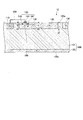
- FIG. 9 shows a configuration of an X-ray detector 1010 configured similarly to the SDD disclosed in Patent Document 1 or Patent Document 2.
- FIG. 9 shows a cross section of the X-ray detector 1010. As shown in FIG. 9, the X-ray detector 1010 has a semiconductor substrate 1100.
- the semiconductor substrate 1100 has a semiconductor layer 1101, an anode electrode 1110, a cathode electrode 1120, and a plurality of regions 1130.
- the reference numeral of one region 1130 is shown as a representative of the plurality of regions 1130.
- the semiconductor substrate 1100 has a surface 1100a and a surface 1100b.
- the surface 1100a and the surface 1100b face in opposite directions.
- the semiconductor layer 1101 includes an N-type semiconductor.
- the anode electrode 1110 and the plurality of regions 1130 are provided in the semiconductor layer 1101.
- Anode electrode 1110 includes an N-type semiconductor.
- the impurity concentration of the anode electrode 1110 is higher than the impurity concentration of the semiconductor layer 1101.
- the region 1130 includes a P-type semiconductor.
- the anode electrode 1110 and the plurality of regions 1130 include a surface 1100a.
- Each of the anode electrode 1110 and the plurality of regions 1130 is a semiconductor region from the surface 1100a to a predetermined depth.
- the cathode electrode 1120 is disposed on the semiconductor layer 1101.
- Cathode electrode 1120 includes a P-type semiconductor.
- Cathode electrode 1120 includes a surface 1100b.
- Cathode electrode 1120 is a semiconductor region from surface 1100b to a predetermined depth.
- a terminal for outputting a signal from the anode electrode 1110 may be provided on the anode electrode 1110.
- a terminal for applying a voltage to the cathode electrode 1120 may be provided on the cathode electrode 1120.
- a plurality of gate electrodes are arranged on surface 1100a. The gate electrode and the region 1130 form a MOSFET (Metal Oxide Semiconductor Semiconductor Field Effect Transistor).
- FIG. 10 is a plan view of the X-ray detector 1010.
- FIG. 10 shows each element when the X-ray detector 1010 is viewed in a direction perpendicular to the surface 1100a of the semiconductor substrate 1100. That is, FIG. 10 shows each element when the X-ray detector 1010 is viewed from the front of the semiconductor substrate 1100.
- the reference numeral of one area 1130 is shown as a representative of the plurality of areas 1130.
- Anode electrode 1110 is arranged at the center of surface 1100a of semiconductor substrate 1100.
- the anode electrode 1110 is circular.
- the plurality of regions 1130 are ring-shaped.
- the plurality of regions 1130 are arranged concentrically.
- the plurality of regions 1130 are arranged so as to surround the anode electrode 1110.
- a cross section taken along line L10 shown in FIG. 10 is shown in FIG.
- a negative voltage is applied to the cathode electrode 1120.
- the absolute value of the voltage applied to cathode electrode 1120 is larger than the absolute value of the voltage of anode electrode 1110.
- the potential inside semiconductor substrate 1100 increases from surface 1100b toward surface 1100a.
- a negative voltage is applied to the gate electrode on surface 1100a.
- the potential of the anode electrode 1110 is higher than any potential of the plurality of gate electrodes.
- the absolute value of the voltage applied to the outer gate electrode is larger than the absolute value of the voltage applied to the inner gate electrode. Therefore, the absolute value of the voltage applied to the outer region 1130 is larger than the absolute value of the voltage applied to the inner region 1130.
- the potential inside semiconductor substrate 1100 increases from the outer periphery of semiconductor substrate 1100 toward the center.
- the voltage as described above is applied to the X-ray detector 1010.
- the potential in the semiconductor substrate 1100 increases from the surface 1100b toward the surface 1100a, and increases from the outer periphery of the semiconductor substrate 1100 toward the center. That is, a potential gradient is generated in the semiconductor substrate 1100.
- X-rays enter the X-ray detector 1010, electrons are generated in the semiconductor substrate 1100. The electrons gather on the anode electrode 1110 according to the potential gradient. A signal based on the electrons is output from X-ray detector 1010.
- a chip having a first-stage amplifier is used to convert the electric charge into a voltage signal.
- the chip having the first-stage amplifier is different from the chip having the X-ray detector.
- the first-stage amplifier is composed of a JFET (Junction Field Effect Transistor) or the like.
- this method requires a wire containing aluminum or gold between the X-ray detector and the first-stage amplifier.
- the wires increase the components of capacitance, resistance, and inductor, and increase noise.
- a technique for forming a JFET at the center of an X-ray detector is known.
- a JFET is arranged at the center of the X-ray detector, and an anode electrode is arranged around the JFET.
- the anode electrode has a ring shape.
- the peripheral length of the anode electrode is larger than in the technique in which the anode electrode is arranged at the center of the X-ray detector. Therefore, the parasitic capacitance on the anode electrode increases, and noise increases.
- An object of the present invention is to provide an X-ray detector capable of suppressing an increase in noise.
- an X-ray detector has a semiconductor substrate, a first electrode, and a second electrode.
- the semiconductor substrate has a first main surface and a second main surface facing in opposite directions.
- the first electrode is arranged on the first main surface, and collects electric charges generated in the semiconductor substrate when X-rays are incident on the semiconductor substrate.
- the second electrode is disposed on the second main surface.
- a voltage for moving the charge in the direction of the first electrode is applied to the second electrode.
- the semiconductor substrate has a third electrode and a transistor.
- the third electrode is arranged in the semiconductor substrate and forms a part of the first main surface.
- a voltage for moving the charge in the direction of the first electrode is applied to the third electrode.
- the transistor has a source, a drain, and a gate. The source and the drain are disposed in the third electrode.
- the gate is disposed on the first main surface and is connected to the first electrode.
- the absolute value of the voltage may be 10 V or less.
- the X-ray detector may include a plurality of the first electrodes and a plurality of the third electrodes.
- the source and the drain may be arranged in the third electrode closest to the first electrode.
- the first voltage may be applied as the voltage to the third electrode on which the transistor is arranged.
- a second voltage may be applied as the voltage to the third electrode where the transistor is not provided.
- the absolute value of the first voltage may be smaller than the absolute value of the second voltage.
- the third electrode may extend from the first main surface to a first position.
- the first position may be separated from the first main surface by a first distance toward the inside of the semiconductor substrate.
- the first electrode may extend from the first main surface to a second position.
- the second position may be separated from the first main surface by a second distance toward the inside of the semiconductor substrate. The first distance may be greater than the second distance.
- the plurality of third electrodes are arranged as a first part and the third electrode arranged as a second part. And the third electrode.
- the first portion may extend from the first main surface to a third position.
- the third position may be separated from the first main surface by a third distance toward the inside of the semiconductor substrate.
- the second portion may extend from the first main surface to a fourth position.
- the fourth position may be separated from the first main surface by a fourth distance toward the inside of the semiconductor substrate.
- the third distance may be greater than the fourth distance.
- the second portion may be arranged between the first electrode and the first portion.
- the source and the drain may be arranged in the second portion.
- the X-ray detector may further include a fourth electrode.
- the fourth electrode may extend from a fifth position to a sixth position.
- the fifth position may be separated from the second main surface by a fifth distance toward the inside of the semiconductor substrate.
- the sixth position may be separated from the second main surface by a sixth distance toward the inside of the semiconductor substrate. The sixth distance may be greater than the fifth distance.
- the second electrode may extend from the second main surface to the fifth position.
- the X-ray detector can suppress an increase in noise.
- FIG. 2 is a sectional view of the X-ray detector according to the first embodiment of the present invention. It is a top view of the X-ray detector of a 1st embodiment of the present invention. It is a sectional view of an X-ray detector of a 2nd embodiment of the present invention. It is sectional drawing of the X-ray detector of 3rd Embodiment of this invention. It is sectional drawing of the X-ray detector of the 1st modification of 3rd Embodiment of this invention. It is sectional drawing of the X-ray detector of the 2nd modification of 3rd Embodiment of this invention. It is a top view of the X-ray detector of a 4th embodiment of the present invention. It is a top view of the X-ray detector of a modification of a 4th embodiment of the present invention. It is sectional drawing of the X-ray detector of a prior art. It is a top view of a conventional X-ray detector.
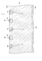
- FIG. 1 shows a configuration of an X-ray detector 10 according to a first embodiment of the present invention.
- FIG. 1 shows a cross section of the X-ray detector 10.
- the X-ray detector 10 is configured as a silicon drift detector (SDD) that detects radiation, that is, fluorescent X-rays.
- SDD silicon drift detector
- the dimensions of the parts constituting the X-ray detector 10 do not always follow the dimensions shown in FIG.
- the dimensions of the parts constituting the X-ray detector 10 may be arbitrary. The same applies to dimensions in other sectional views.
- the X-ray detector 10 has a semiconductor substrate 100, an anode electrode 110 (first electrode), and a cathode electrode 120 (second electrode).
- Semiconductor substrate 100 has a surface 100a (first main surface) and a surface 100b (second main surface) that face in opposite directions.
- the anode electrode 110 is disposed on the surface 100a, and collects charges generated in the semiconductor substrate 100 when X-rays enter the semiconductor substrate 100.
- Cathode electrode 120 is arranged on surface 100b. A voltage for moving the charges in the direction of the anode electrode 110 is applied to the cathode electrode 120.
- the semiconductor substrate 100 includes a region 130 (third electrode) and a transistor 140.
- the region 130 is arranged in the semiconductor substrate 100 and forms a part of the surface 100a.
- a voltage for moving charges in the direction of the anode electrode 110 is applied to the region 130.
- the transistor 140 has a source 141, a drain 142, and a gate 143. Source 141 and drain 142 are arranged in region 130.
- Gate 143 is arranged on surface 100a. Gate 143 is connected to anode electrode 110.
- the semiconductor substrate 100 has a semiconductor layer 101, an anode electrode 110, a cathode electrode 120, and a plurality of regions 130.
- the semiconductor material forming the semiconductor substrate 100 is silicon (Si).
- Surface 100a and surface 100b constitute a main surface of semiconductor substrate 100.
- the main surface is a relatively wide surface among a plurality of surfaces constituting the surface of the semiconductor substrate 100.
- the semiconductor layer 101 includes an N-type semiconductor.
- the anode electrode 110 and the plurality of regions 130 are arranged on the semiconductor layer 101.
- Anode electrode 110 includes an N-type semiconductor.
- the impurity concentration of the anode electrode 110 is higher than the impurity concentration of the semiconductor layer 101.
- the region 130 includes a P-type semiconductor.
- Anode electrode 110 and region 130 include surface 100a. Each of anode electrode 110 and region 130 is a semiconductor region from surface 100a to a predetermined depth. The area 130 extends from the surface 100a to a predetermined position. The predetermined position is separated from the surface 100a toward the inside of the semiconductor substrate 100 by a distance d1. The distance d1 is the depth of the region 130.
- the transistor 140 is a MOSFET.
- the source 141 and the drain 142 are arranged in the region 130 closest to the anode electrode 110.
- Source 141 and drain 142 are arranged in region 130 adjacent to anode electrode 110.
- the region 130 where the source 141 is disposed is the same as the region 130 where the drain 142 is disposed.
- a drain 142 is arranged on a side closer to the anode electrode 110, and a source 141 is arranged on a side farther from the anode electrode 110.
- the drain 142 is disposed between the anode electrode 110 and the source 141.
- the source 141 and the drain 142 include an N-type semiconductor.
- Source 141 and drain 142 include surface 100a. Each of source 141 and drain 142 is a semiconductor region from surface 100a to a predetermined depth.
- the source 141 extends from the surface 100a to a predetermined position. The predetermined position of the source 141 is away from the surface 100a by a distance d2 toward the inside of the semiconductor substrate 100.
- the drain 142 extends from the surface 100a to a predetermined position.
- the predetermined position of the drain 142 is away from the surface 100a by a distance d3 toward the inside of the semiconductor substrate 100.
- the distance d2 is the same as the distance d3.
- the distance d2 may be different from the distance d3.
- the distance d2 and the distance d3 are smaller than the distance d1.
- the distance d2 is the depth of the source 141.
- the distance d3 is the depth of the drain 142.
- An insulating layer 150 is arranged on a region between the source 141 and the drain 142.
- the insulating layer 150 is made of an insulating material.
- the insulating material forming the insulating layer 150 is silicon dioxide (SiO2).
- the insulating layer 150 is stacked on the semiconductor layer 101.
- the insulating layer 150 is in contact with the surface 100a.
- the gate 143 is stacked on the insulating layer 150. Gate 143 is connected to anode electrode 110 by wiring 160.
- the region 130 where the gate 143 is arranged is the same as the region 130 where the source 141 and the drain 142 are arranged.
- the source 141 and the drain 142 are connected to a wiring not shown in FIG.
- the source 141 and the drain 142 are electrically connected to a circuit outside the X-ray detector 10.
- the transistor 140 is a circuit element for extracting a signal from the anode electrode 110 and amplifying the signal. By disposing the transistor 140 in the X-ray detector 10, a first-stage amplifier including the transistor 140 can be disposed in the X-ray detector 10.
- the cathode electrode 120 is disposed on the semiconductor layer 101.
- Cathode electrode 120 includes a P-type semiconductor.
- Cathode electrode 120 includes surface 100b.
- Cathode electrode 120 is a semiconductor region from surface 100b to a predetermined depth.
- a terminal for outputting a signal from the anode electrode 110 may be provided on the anode electrode 110.
- a terminal for applying a voltage to the cathode electrode 120 may be disposed on the cathode electrode 120.
- a plurality of gate electrodes are arranged on surface 100a.
- the gate electrode and the region 130 constitute a MOSFET. This MOSFET is a PMOS, and the transistor 140 is an NMOS.
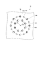
- FIG. 2 is a plan view of the X-ray detector 10.
- FIG. 2 shows each element when the X-ray detector 10 is viewed in a direction perpendicular to the surface 100a of the semiconductor substrate 100. That is, in FIG. 2, each element when the X-ray detector 10 is viewed from the front of the semiconductor substrate 100 is shown.
- the reference numeral of one area 130 is shown as a representative of the plurality of areas 130.
- the outer shape of the X-ray detector 10 is rectangular. In the example shown in FIG. 2, the outer shape of the X-ray detector 10 is a square. The outer shape of the X-ray detector 10 is not limited to a rectangle.
- the anode electrode 110 is arranged at the center of the surface 100 a of the semiconductor substrate 100.
- the anode electrode 110 is circular.
- the outer shape of the anode electrode 110 may be rectangular or the like.
- the plurality of regions 130 are ring-shaped.
- the plurality of regions 130 are arranged concentrically.
- the plurality of regions 130 are arranged so as to surround the anode electrode 110.
- a cross section through the line L1 shown in FIG. 2 is shown in FIG.
- a negative voltage is applied to the cathode electrode 120.
- the absolute value of the voltage applied to the cathode electrode 120 is larger than the absolute value of the voltage of the anode electrode 110.
- the voltage applied to the cathode electrode 120 is from ⁇ 80V to ⁇ 100V.
- the potential inside semiconductor substrate 100 increases from surface 100b toward surface 100a.
- a negative voltage is applied to the gate electrode on the surface 100a.
- the potential of the anode electrode 110 is higher than any potential of the plurality of gate electrodes.
- the absolute value of the voltage applied to the outer gate electrode is larger than the absolute value of the voltage applied to the inner gate electrode. Therefore, the absolute value of the voltage applied to the outer region 130 is larger than the absolute value of the voltage applied to the inner region 130.
- the voltage applied to the outermost region 130 is between -80V and -100V.
- the potential inside the semiconductor substrate 100 increases from the outer periphery to the center of the semiconductor substrate 100.
- the first voltage is applied to the region 130 where the transistor 140 is provided.
- a second voltage is applied to region 130 where transistor 140 is not located.
- the absolute value of the first voltage is smaller than the absolute value of the second voltage.
- a voltage having an absolute value of 10 V or less is applied to the region 130 where the transistor 140 is provided. For example, a voltage in the range of ⁇ 5 V to ⁇ 10 V is applied to the region 130. A voltage in the range of -1V to -10V may be applied to the region 130.
- the voltage as described above is applied to the X-ray detector 10.
- the potential in the semiconductor substrate 100 increases from the surface 100b toward the surface 100a, and increases from the outer periphery to the center of the semiconductor substrate 100. That is, a potential gradient is generated in the semiconductor substrate 100.
- X-rays enter the X-ray detector 10 electrons are generated in the semiconductor substrate 100.
- the electrons gather on the anode electrode 110 according to the potential gradient.
- a signal based on the electrons is extracted by the transistor 140.
- the semiconductor substrate 100 may include a P-type semiconductor.
- the anode electrode 110, the source 141, and the drain 142 include a P-type semiconductor.
- the cathode electrode 120 and the region 130 include an N-type semiconductor.
- a positive voltage is applied to the cathode electrode 120 and the region 130.
- holes are output from the anode electrode 110 as charges.
- the X-ray detector 10 according to the first embodiment has the transistor 140 arranged in the region 130 in the semiconductor substrate 100. Therefore, the peripheral length of the anode electrode 110 does not increase.
- the X-ray detector 10 can suppress an increase in noise caused by the parasitic capacitance of the anode electrode 110.
- the transistor 140 is disposed in the region 130 closest to the anode electrode 110.
- a relatively low voltage (a voltage having a small absolute value) is applied to the region 130 where the transistor 140 is provided. Since the withstand voltage of the transistor 140 is easily ensured, the thickness of the insulating layer 150 can be reduced, and the transistor 140 can be easily formed.
- a plurality of electrons generated by X-rays are not always accelerated uniformly by a potential gradient.
- the speed of the plurality of electrons varies. Therefore, the difference in the time when a plurality of electrons reach the anode electrode in the X-ray detector increases. If the difference is large, the signal output from the anode electrode is processed as noise by the subsequent signal processing circuit. The signal is not suitable for analysis.
- FIG. 3 shows a configuration of the X-ray detector 11 according to the second embodiment of the present invention.
- FIG. 3 shows a cross section of the X-ray detector 11. The description of the same parts as those shown in FIG. 1 is omitted.
- the X-ray detector 11 has a plurality of anode electrodes 110.
- three anode electrodes 110 are shown.
- a region 130 is arranged between two adjacent anode electrodes 110.
- two regions 130 are shown.
- a transistor 140 is provided in each region 130.
- the number of anode electrodes 110 and the number of regions 130 are the same.
- the voltages applied to the plurality of anode electrodes 110 are the same.
- one anode electrode 110 can be made smaller. Therefore, the parasitic capacitance on the anode electrode 110 decreases.
- a plurality of anode electrodes 110 are separated from each other by each region 130.
- a potential gradient is generated in a direction from each region 130 toward the anode electrode 110.
- the electrons move to the anode electrode 110 according to the potential gradient.
- a plurality of electrons included in one electron group are difficult to separate and easily reach one anode electrode 110.
- FIG. 4 shows a configuration of the X-ray detector 12 according to the third embodiment of the present invention.
- FIG. 4 shows a cross section of the X-ray detector 12. The description of the same portions as those shown in FIG. 1 or 3 will be omitted.
- the region 131 extends from the surface 100a to a predetermined position (first position).
- the predetermined position is separated from the surface 100a toward the inside of the semiconductor substrate 100 by a distance d4 (first distance).
- the distance d4 is larger than the distance d1 shown in FIG.
- the anode electrode 110 extends from the surface 100a to a predetermined position (second position).
- the predetermined position is separated from the surface 100a toward the inside of the semiconductor substrate 100 by a distance d5 (second distance).
- the distance d4 is larger than the distance d5.
- the distance d4 is the depth of the region 131.
- the distance d5 is the depth of the anode electrode 110.
- the region 130 shown in FIG. 3 is formed by ion implantation.
- the region 131 shown in FIG. 4 is formed by, for example, the following method. A hole is dug deep into the semiconductor layer 101, and the surface of the hole is covered with an insulating layer. Then, a conductor layer is formed in the hole covered with the insulating layer. When an appropriate voltage is applied to the region 131, an inversion layer is formed at the interface between the insulating layer and the semiconductor layer 101, as in the ON state of the MOSFET. The inversion layer has a polarity opposite to the polarity of the anode electrode 110.
- FIG. 5 shows a configuration of an X-ray detector 13 according to a first modification of the third embodiment of the present invention.
- FIG. 5 shows a cross section of the X-ray detector 13. The description of the same parts as those shown in FIG. 4 will be omitted.
- the area 131 shown in FIG. The transistor 140 is not provided in the region 132.
- An area 130 is arranged in addition to the area 132.
- the transistor 140 is provided in the region 130.
- the region 132 (first portion) extends from the surface 100a to a predetermined position (third position). The predetermined position is away from the surface 100a toward the inside of the semiconductor substrate 100 by a distance d6 (third distance).
- the region 130 (second portion) extends from the surface 100a to a predetermined position (fourth position).
- the predetermined position is separated from the surface 100a by a distance d1 (fourth distance) toward the inside of the semiconductor substrate 100.
- the distance d6 is larger than the distance d1.
- the distance d6 is the depth of the region 132.
- Region 130 is arranged between anode electrode 110 and region 132.
- the region 132 is arranged between two adjacent anode electrodes 110.
- the voltage applied to the region 132 and the voltage applied to the region 130 are different from each other.
- the absolute value of the voltage applied to the region 132 is larger than the absolute value of the voltage applied to the region 130.
- the absolute value of the voltage applied to the cathode electrode 120 can be reduced as in the X-ray detector 12 shown in FIG.
- FIG. 6 shows a configuration of an X-ray detector 14 according to a second modification of the third embodiment of the present invention.
- FIG. 6 shows a cross section of the X-ray detector 14. The description of the same parts as those shown in FIG. 4 will be omitted.
- the X-ray detector 14 further has a plurality of regions 170 (fourth electrodes). In FIG. 6, two regions 170 are shown.
- the region 170 is provided in the semiconductor layer 101.
- Region 170 includes a P-type semiconductor.
- the region 170 is a semiconductor region from the interface between the cathode electrode 120 and the semiconductor layer 101 to a predetermined depth.
- Cathode electrode 120 extends from surface 100b to position P1 (fifth position).
- the position P1 is separated from the surface 100b toward the inside of the semiconductor substrate 100 by a distance d7 (fifth distance).
- the region 170 extends from the position P1 to a position P2 (sixth position).
- the position P2 is separated from the surface 100b toward the inside of the semiconductor substrate 100 by a distance d8 (sixth distance).
- the distance d8 is larger than the distance d7.
- the distance d7 is the depth of the cathode electrode 120.
- the distance d8 is the depth of the region 170.
- the position of the region 170 in the direction Dr1 parallel to the surface 100a and the position of the region 131 in the direction Dr1 are the same.
- the virtual straight line VL1 passes through the region 170 and the region 131.
- the virtual straight line VL1 extends in a direction Dr2 perpendicular to the surface 100a.
- the direction Dr2 is a thickness direction of the semiconductor substrate 100.
- the position of the region 170 in the direction Dr1 and the position of the region 131 in the direction Dr1 may be different.
- Region 170 is connected to cathode electrode 120.
- the voltage applied to cathode electrode 120 is applied to region 170.
- the region 131 and the region 170 may be connected. That is, the region 131 and the region 170 may be formed as layers penetrating the semiconductor substrate 100. At least one of the X-ray detector 10 shown in FIG. 1, the X-ray detector 11 shown in FIG. 3, and the X-ray detector 13 shown in FIG.
- Forming the region 170 deep reduces the area that must be depleted between the region 170 and the region 131. Therefore, the voltage applied to cathode electrode 120 can be reduced. In other words, the absolute value of the voltage applied to the cathode electrode 120 can be reduced.
- FIG. 7 is a plan view of an X-ray detector 15 according to the fourth embodiment of the present invention.
- FIG. 7 shows each element when the X-ray detector 15 is viewed in a direction perpendicular to the surface 100a of the semiconductor substrate 100. That is, in FIG. 7, each element when the X-ray detector 15 is viewed from the front of the semiconductor substrate 100 is shown.
- the X-ray detector 15 has a plurality of anode electrodes 110 and a plurality of regions 130.
- the reference numeral of one anode electrode 110 is shown as a representative of the plurality of anode electrodes 110.
- the reference numeral of one area 130 is shown as a representative of the plurality of areas 130.
- the plurality of anode electrodes 110 are arranged around the area 100c on the surface 100a.
- the plurality of anode electrodes 110 are arranged at equal intervals.
- the distance from the center of the region 100c to the plurality of anode electrodes 110 is the same.
- the plurality of regions 130 extend radially from the center of the region 100c.
- Each region 130 is arranged between two adjacent anode electrodes 110.
- the plurality of anode electrodes 110 and the plurality of regions 130 are arranged symmetrically.
- the transistor 140 is arranged in the portion 130 a of the region 130.
- the portion 130a is disposed between two adjacent anode electrodes 110.
- the plurality of anode electrodes 110 and the plurality of regions 130 are arranged without bias. Therefore, the performance of each of the anode electrodes 110 to detect electrons becomes uniform.
- FIG. 8 is a plan view of an X-ray detector 16 according to a modification of the fourth embodiment of the present invention.
- FIG. 8 shows each element when the X-ray detector 16 is viewed in a direction perpendicular to the surface 100a of the semiconductor substrate 100. That is, FIG. 8 shows each element when the X-ray detector 16 is viewed from the front of the semiconductor substrate 100.
- the X-ray detector 16 has a plurality of anode electrodes 110 and a plurality of regions 130.
- reference numeral of one anode electrode 110 is shown as a representative of the plurality of anode electrodes 110.
- reference numerals of two regions 130 are shown as representatives of the plurality of regions 130.
- the positions of the plurality of anode electrodes 110 are the same as the positions of the plurality of anode electrodes 110 shown in FIG.
- the plurality of regions 130 include a first group of eight regions 130 and a second group of eight regions 130.
- the eight regions 130 of the first group are arranged at positions separated by a distance d9 from the center of the region 100c.
- Each region 130 of the first group is arranged between two adjacent anode electrodes 110.
- the eight regions 130 of the second group are arranged at positions separated by a distance d10 from the center of the region 100c.
- the distance d10 is smaller than the distance d9.
- the eight regions 130 of the first group are arranged at equal intervals.
- the eight regions 130 of the second group are arranged at equal intervals.
- the plurality of anode electrodes 110 and the plurality of regions 130 are arranged symmetrically.
- the transistor 140 is arranged in each region 130 of the first group.
- the plurality of anode electrodes 110 and the plurality of regions 130 are arranged without bias. Therefore, the performance of each of the anode electrodes 110 to detect electrons becomes uniform.
- the X-ray detector can suppress an increase in noise.
Landscapes
- Physics & Mathematics (AREA)
- Health & Medical Sciences (AREA)
- Life Sciences & Earth Sciences (AREA)
- General Physics & Mathematics (AREA)
- High Energy & Nuclear Physics (AREA)
- Molecular Biology (AREA)
- Spectroscopy & Molecular Physics (AREA)
- Measurement Of Radiation (AREA)
Abstract
La présente invention concerne un détecteur par rayons X comprenant un substrat semi-conducteur, une première électrode et une seconde électrode. La première électrode est placée sur une première surface principale du substrat semi-conducteur. La deuxième électrode est placée sur une seconde surface principale du substrat semi-conducteur. Le substrat semi-conducteur comporte une troisième électrode et un transistor. La troisième électrode est placée à l'intérieur du substrat semi-conducteur, formant une partie de la première surface principale, et une tension destinée à déplacer une charge dans la direction de la première électrode est appliquée. Le transistor comprend une source, un drain, et une grille. La source et le drain sont placés à l'intérieur de la troisième électrode. La grille est placée sur la première surface principale, et est connectée à la première électrode.
Priority Applications (1)
| Application Number | Priority Date | Filing Date | Title |
|---|---|---|---|
| PCT/JP2018/025235 WO2020008531A1 (fr) | 2018-07-03 | 2018-07-03 | Détecteur par rayons x |
Applications Claiming Priority (1)
| Application Number | Priority Date | Filing Date | Title |
|---|---|---|---|
| PCT/JP2018/025235 WO2020008531A1 (fr) | 2018-07-03 | 2018-07-03 | Détecteur par rayons x |
Publications (1)
| Publication Number | Publication Date |
|---|---|
| WO2020008531A1 true WO2020008531A1 (fr) | 2020-01-09 |
Family
ID=69059542
Family Applications (1)
| Application Number | Title | Priority Date | Filing Date |
|---|---|---|---|
| PCT/JP2018/025235 Ceased WO2020008531A1 (fr) | 2018-07-03 | 2018-07-03 | Détecteur par rayons x |
Country Status (1)
| Country | Link |
|---|---|
| WO (1) | WO2020008531A1 (fr) |
Citations (4)
| Publication number | Priority date | Publication date | Assignee | Title |
|---|---|---|---|---|
| JPH11186285A (ja) * | 1997-12-22 | 1999-07-09 | Rigaku Industrial Co | 半導体装置 |
| JP2008258348A (ja) * | 2007-04-04 | 2008-10-23 | Institute X-Ray Technologies Co Ltd | 放射線検出器 |
| US20090026569A1 (en) * | 2007-07-27 | 2009-01-29 | Shenzhen Skyray Instrument Co., Ltd. | Ultra high-resolution radiation detector (UHRD) and method for fabrication thereof |
| JP2014002155A (ja) * | 2012-06-20 | 2014-01-09 | Oxford Instruments Analytical Oy | 漏れ電流収集構造およびそれを用いた放射線検出器 |
-
2018
- 2018-07-03 WO PCT/JP2018/025235 patent/WO2020008531A1/fr not_active Ceased
Patent Citations (4)
| Publication number | Priority date | Publication date | Assignee | Title |
|---|---|---|---|---|
| JPH11186285A (ja) * | 1997-12-22 | 1999-07-09 | Rigaku Industrial Co | 半導体装置 |
| JP2008258348A (ja) * | 2007-04-04 | 2008-10-23 | Institute X-Ray Technologies Co Ltd | 放射線検出器 |
| US20090026569A1 (en) * | 2007-07-27 | 2009-01-29 | Shenzhen Skyray Instrument Co., Ltd. | Ultra high-resolution radiation detector (UHRD) and method for fabrication thereof |
| JP2014002155A (ja) * | 2012-06-20 | 2014-01-09 | Oxford Instruments Analytical Oy | 漏れ電流収集構造およびそれを用いた放射線検出器 |
Non-Patent Citations (2)
| Title |
|---|
| MATSUURA, HIDEHARU ET AL.: "A new n-channel junction field-effect transistor embedded in the i layer of a pin diode", JAPANESE JOURNAL OF APPLIED PHYSICS, vol. 38, 1999, pages L1015 - L1017, XP000948575, DOI: 10.1143/JJAP.38.L1015 * |
| MATSUURA, HIDEHARU ET AL.: "A new structure of an n-channel junction field-effect transistor embedded in a pin diode for an x-ray detector", JAPANESE JOURNAL OF APPLIED PHYSICS, vol. 37, 1998, pages L115 - L118, XP000824541, DOI: 10.1143/JJAP.37.L115 * |
Similar Documents
| Publication | Publication Date | Title |
|---|---|---|
| US6455858B1 (en) | Semiconductor radiation detector | |
| WO2018061334A1 (fr) | Photodiode à avalanche | |
| JP6393347B2 (ja) | 電荷検出増幅器 | |
| US7105827B2 (en) | Semiconductor detector with optimised radiation entry window | |
| US10951174B2 (en) | High-frequency amplifier | |
| IL192209A (en) | Semiconductor radiation detector optimized for detecting visible light | |
| CN105575984B (zh) | 特别用途的背照式光传感器集成电路接地系统 | |
| WO2016143156A1 (fr) | Détecteur de rayonnement et dispositif de détection de rayonnement l'utilisant | |
| CN101300685A (zh) | 半导体装置及其制造方法 | |
| EP3032281B1 (fr) | Détecteur de dérive à semi-conducteur pour détecter un rayonnement | |
| WO2020008531A1 (fr) | Détecteur par rayons x | |
| JP6909057B2 (ja) | 炭化ケイ素半導体装置およびその製造方法 | |
| US11604292B2 (en) | Charge preamplifier device and radiation detecting apparatus comprising the device | |
| JP4267397B2 (ja) | 信号電子検出器 | |
| WO2019123591A1 (fr) | Dispositif semi-conducteur | |
| CN106328661B (zh) | 一种x射线传感器及其制造方法 | |
| US20250306221A1 (en) | Semiconductor detector | |
| RU2141703C1 (ru) | Способ осуществления внутреннего пропорционального усиления в полупроводниковом детекторе частиц и излучений и устройство для его реализации | |
| WO2020183567A1 (fr) | Dispositif de détection de rayons x et dispositif d'analyse de fluorescence de rayons x | |
| RU2583955C1 (ru) | Емкостная моп диодная ячейка фотоприемника-детектора излучений | |
| JP2005043263A (ja) | 信号検出器 | |
| JP2024515298A (ja) | ダイオード放射線センサ | |
| JP6493158B2 (ja) | X線検出器 | |
| US20200220079A1 (en) | Compound semiconductor device | |
| CN119486291A (zh) | 一种双埋氧绝缘体上硅总剂量辐照探测器 |
Legal Events
| Date | Code | Title | Description |
|---|---|---|---|
| 121 | Ep: the epo has been informed by wipo that ep was designated in this application |
Ref document number: 18925210 Country of ref document: EP Kind code of ref document: A1 |
|
| NENP | Non-entry into the national phase |
Ref country code: DE |
|
| 122 | Ep: pct application non-entry in european phase |
Ref document number: 18925210 Country of ref document: EP Kind code of ref document: A1 |
|
| NENP | Non-entry into the national phase |
Ref country code: JP |