EP2020749A2 - Treiberschaltung zur Ansteuerung eines Leistungshalbleiterschalters - Google Patents
Treiberschaltung zur Ansteuerung eines Leistungshalbleiterschalters Download PDFInfo
- Publication number
- EP2020749A2 EP2020749A2 EP08012363A EP08012363A EP2020749A2 EP 2020749 A2 EP2020749 A2 EP 2020749A2 EP 08012363 A EP08012363 A EP 08012363A EP 08012363 A EP08012363 A EP 08012363A EP 2020749 A2 EP2020749 A2 EP 2020749A2
- Authority
- EP
- European Patent Office
- Prior art keywords
- voltage
- output
- input
- driver circuit
- reference potential
- Prior art date
- Legal status (The legal status is an assumption and is not a legal conclusion. Google has not performed a legal analysis and makes no representation as to the accuracy of the status listed.)
- Granted
Links
Images

Classifications
-
- H—ELECTRICITY
- H03—ELECTRONIC CIRCUITRY
- H03K—PULSE TECHNIQUE
- H03K17/00—Electronic switching or gating, i.e. not by contact-making and –breaking
- H03K17/51—Electronic switching or gating, i.e. not by contact-making and –breaking characterised by the components used
- H03K17/56—Electronic switching or gating, i.e. not by contact-making and –breaking characterised by the components used by the use, as active elements, of semiconductor devices
- H03K17/567—Circuits characterised by the use of more than one type of semiconductor device, e.g. BIMOS, composite devices such as IGBT
-
- H—ELECTRICITY
- H03—ELECTRONIC CIRCUITRY
- H03K—PULSE TECHNIQUE
- H03K17/00—Electronic switching or gating, i.e. not by contact-making and –breaking
- H03K17/06—Modifications for ensuring a fully conducting state
- H03K17/063—Modifications for ensuring a fully conducting state in field-effect transistor switches
-
- H—ELECTRICITY
- H03—ELECTRONIC CIRCUITRY
- H03K—PULSE TECHNIQUE
- H03K17/00—Electronic switching or gating, i.e. not by contact-making and –breaking
- H03K17/51—Electronic switching or gating, i.e. not by contact-making and –breaking characterised by the components used
- H03K17/56—Electronic switching or gating, i.e. not by contact-making and –breaking characterised by the components used by the use, as active elements, of semiconductor devices
- H03K17/687—Electronic switching or gating, i.e. not by contact-making and –breaking characterised by the components used by the use, as active elements, of semiconductor devices the devices being field-effect transistors
- H03K17/6877—Electronic switching or gating, i.e. not by contact-making and –breaking characterised by the components used by the use, as active elements, of semiconductor devices the devices being field-effect transistors the control circuit comprising active elements different from those used in the output circuit
-
- H—ELECTRICITY
- H03—ELECTRONIC CIRCUITRY
- H03K—PULSE TECHNIQUE
- H03K19/00—Logic circuits, i.e. having at least two inputs acting on one output; Inverting circuits
- H03K19/0175—Coupling arrangements; Interface arrangements
- H03K19/018—Coupling arrangements; Interface arrangements using bipolar transistors only
- H03K19/01806—Interface arrangements
-
- H—ELECTRICITY
- H03—ELECTRONIC CIRCUITRY
- H03K—PULSE TECHNIQUE
- H03K17/00—Electronic switching or gating, i.e. not by contact-making and –breaking
- H03K17/16—Modifications for eliminating interference voltages or currents
- H03K17/161—Modifications for eliminating interference voltages or currents in field-effect transistor switches
- H03K17/162—Modifications for eliminating interference voltages or currents in field-effect transistor switches without feedback from the output circuit to the control circuit
- H03K17/163—Soft switching
-
- H—ELECTRICITY
- H03—ELECTRONIC CIRCUITRY
- H03K—PULSE TECHNIQUE
- H03K17/00—Electronic switching or gating, i.e. not by contact-making and –breaking
- H03K17/06—Modifications for ensuring a fully conducting state
- H03K2017/066—Maximizing the OFF-resistance instead of minimizing the ON-resistance
-
- H—ELECTRICITY
- H03—ELECTRONIC CIRCUITRY
- H03K—PULSE TECHNIQUE
- H03K2217/00—Indexing scheme related to electronic switching or gating, i.e. not by contact-making or -breaking covered by H03K17/00
- H03K2217/0063—High side switches, i.e. the higher potential [DC] or life wire [AC] being directly connected to the switch and not via the load
-
- H—ELECTRICITY
- H03—ELECTRONIC CIRCUITRY
- H03K—PULSE TECHNIQUE
- H03K2217/00—Indexing scheme related to electronic switching or gating, i.e. not by contact-making or -breaking covered by H03K17/00
- H03K2217/0072—Low side switches, i.e. the lower potential [DC] or neutral wire [AC] being directly connected to the switch and not via the load
-
- H—ELECTRICITY
- H03—ELECTRONIC CIRCUITRY
- H03K—PULSE TECHNIQUE
- H03K2217/00—Indexing scheme related to electronic switching or gating, i.e. not by contact-making or -breaking covered by H03K17/00
- H03K2217/0081—Power supply means, e.g. to the switch driver
Definitions
- the invention relates to a driver circuit which serves to drive a power semiconductor switch.
- Power semiconductor switches e.g. An IGBT (insulated gate bipolar transistor) must receive a switching signal to perform a switching operation. This is usually done by a logic circuit, e.g. a PLD (Programmable Logic Device).
- An IGBT is e.g. switched on with a voltage of +15 V and with a voltage of e.g. -15 V off. The peak current for switching the gate of the IGBT may be several amperes.
- the programmable logic operates here, e.g. in a range between ground and 3.3V, delivering signals in the range of currents less mA.
- the logic circuit itself therefore provides with its control signal neither enough power nor enough voltage available to actually switch the power semiconductor switch can.
- the currents and voltages supplied by the programmable logic must therefore be amplified in order to actually switch the power semiconductor switch. To amplify the logic signal, a corresponding output stage or driver circuit is required.
- Object of the present invention is to provide an improved driver circuit or power amplifier for the intermediate connection between a programmable logic and a power semiconductor switch.
- the invention is based on the recognition that a power semiconductor switch to be triggered by the driver circuit according to the invention requires a signal of a first voltage against a reference potential - generally ground - in order to be switched on and a signal of a second voltage against this reference potential needed to be switched off to be able to.
- a logic circuit is available for driving the power semiconductor switch, which is supplied between a third voltage and the reference potential and thus can provide switching signals with voltages between the reference potential and the third voltage.
- the invention is achieved by a driver circuit having a first and a second output.
- the first output is used to drive the power semiconductor switch with a signal of the first voltage
- the second output is used to drive the power semiconductor switch with a signal of the second voltage, respectively against the reference potential.
- the driver circuit also has a first and second input, which can be controlled by the logic circuit.
- One Driving the first input causes a switching signal at the first output and a drive at the second input a switching signal at the second output.
- the driver circuit includes a power-on path having the first input and the first output.
- the switch-on path is supplied with the first voltage and the reference potential.
- the driver circuit further includes a turn-off path having the second input and the second output and which is powered by the third voltage and the second voltage.
- On and Ausschaltpfad each for themselves, each have a level converter, which in turn contains the first or second input, depending on the on or off path. Both paths have a current amplifier driven by the respective level converter and a respective output stage controlled by the current amplifier. The respective output stage of the respective path contains the first or second output.
- the entire driver circuit thus has the advantage that it only needs to be supplied by the voltages required anyway for driving the power semiconductor switch, namely the first to third voltage and the reference potential. An additional power supply is not necessary.
- the respective An Kunststoffpfad, so on or off path can be controlled directly from the logic circuit, ie be driven with signals in the range between the reference potential and the third voltage and still deliver at their outputs a switching signal of the first voltage against the reference potential for turning on the power semiconductor switch and the second voltage against the reference potential for turning off the power semiconductor switch.
- the level converter, the current amplifier and the power amplifier can each be designed discretely.
- a discrete design that is, the use of non-integrated or low-integrated devices, e.g. Bipolar or MOSFET transistors, in discrete interconnection, are much less expensive than using a fully integrated drive module mentioned above.
- the level converter may include a connected to its control input to the respective input of the input or Ausschaltpfades transistor with series resistors.
- the transistor with the collector and emitter is then guided via a respective ohmic resistance to the two supplying voltages of the respective path, the base is guided to the respective input and an input resistance is connected between the base and the emitter.
- the current amplifier may be an emitter follower containing two transistors.
- the collector terminal of the transistor of the level converter is then performed in parallel on two bases of two transistors, which are connected with their collectors and emitters connected in series between the two, the respective path supplying voltages.
- the output stage can contain a MOSFET with series resistor connected to its output with its output.
- the source terminal of the MOSFET is then connected to the respective first or second voltage in the respective path, the drain terminal is connected to the output, the gate is connected to the mutually connected emitters of the emitter follower and between gate and Source is an ohmic input resistance connected.
- the first voltage is preferably + 15V
- the reference potential is preferably ground.
- Such voltage constellations are e.g. for the operation of an IGBT by a corresponding PLD logic circuit usual voltage values.
- the logic circuit can be a PLD.
- the driver circuit may be one for driving an IGBT as a power semiconductor switch.
- Fig. 1 shows a semiconductor switch assembly, consisting of an IGBT 2 as a semiconductor switch, a driving this driver 4 and a power supply 6 for the driver 4 and for driving the IGBT second
- the driver 4 comprises a PLD 8, which provides the logical control functionality for the IGBT 2, and two separate drive channels 10a and 10b driven by the PLD 8.
- the control channel 10a serves to turn on the IGBT 2 and is connected to its output 12a via a resistor RGON to the control input 14 of the IGBT 2.
- the control channel 10b is used to turn off the IGBT 2 and is also connected to its output 12b via a resistor ROFF to the control input 14.
- Each control channel 10a, b in this case contains in each case a semiconductor switch S1 and S2, which are controlled by the PLD 8 and the respective resistors RGON and ROFF a respective turn-on voltage U VP of +15 V or a turn-off voltage U VN from -8V to -15V switch the control input 14 of the IGBT.
- Both voltages U VP and U VN are part of the voltage supply 6, which also provides a logic voltage U L of + 3.3V available, with which primarily the PLD 8 is operated.
- the reference potential for all voltages is ground GND.
- the drive channel 10a is supplied by the supply voltage U VP to ground GND.
- the drive channel 10b is supplied by the logic voltage U L against the (negative) switch-off voltage U VN .
- the PLD 8 generates control voltages, which are supplied via the control lines 16a, b to the respective inputs 18a, b of the drive channels 10a, b and in the range between 0V, that is GND and the logic voltage U L of + 3.3V.
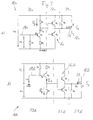
- Fig. 2 shows the Anêtäle 10a, b in more detail or block diagram.
- Each of the drive channels 10a, b is constructed from the respective input 18a, b to the output 12a, b in the same way, namely as a series circuit of a level converter 20a, b, a current amplifier 22a, b and an output stage 24a, b.
- the drive channel 10a contains as transistor S 1 a P-channel field-effect transistor in the output stage 24a, the control channel 10b as transistor S 2 an N-channel field-effect transistor in the output stage 24b.
- the temporal overlap of the two switched on and off output transistors S 1 and S 2 is realized via the inputs 18 a, b, so by the PLD 8 as a running therein, not shown program.
- Fig. 3a shows in a more detailed representation of the control channel 10a; Fig. 3b the drive channel 10b.
- the input resistance R 1 between the base B of the transistor Q 1 and ground GND is required in order to set the base B of the transistor Q 1 to a defined potential, namely ground GND, in the case of a high-impedance triggering stage, ie a high-resistance output of the PLD 8 so that the transistor Q 1 remains safely off.
- a positive drive voltage U IN from PLD 8 at base B of Q 1 turns on transistor Q 1 and allows a defined collector current to flow through transistor Q 1 .
- This stream is impressed by the input voltage U IN and the resistor R 2 .
- the resistor R 3 drops a defined voltage U 3 .
- This voltage U 3 is amplified by the downstream emitter follower 26 a, consisting of the transistors Q 2 and Q 3 , and thus the gate G of S 1 is charged.
- the voltage across the resistor R 4 rises and turns on the transistor S 1 when exceeding its input threshold.
- the switch represented by the transistor S 1 closes.
- the IGBT 2 is switched on.
- the power output 28 of the transistor S 1 is active.
- the input voltage U IN at the base of the transistor Q 1 drops to GND potential, the current flow through the transistor Q 1 decreases, and the voltage U 3 at R 3 decreases.
- the voltage U 3 is amplified by the downstream emitter follower 26 b, the gate G discharged from S 1 and pulled to the potential of U vp .
- the switch-on threshold of S 1 is undershot, the output stage transistor S 1 begins to block.
- the switch represented by S 1 opens.
- the IGBT 2 is no longer supplied with a switch-on pulse of the voltage U VP .
- the power output 28 of the transistor S 1 runs empty.
- the resistor R 4 between gate G and source S of S 1 discharges the gate G completely, so that in the off state of S 1 no voltage between gate G and source S is applied.
- the input resistance R 5 between the base B of the transistor Q 5 and the voltage U L is required to in the case of a high-impedance output of the PLD 8 and thus at the base B of the transistor Q 5 just this base B to a defined potential, namely Voltage U L , so that the transistor Q 5 remains safely off.
- the power amp transistor S 2 is namely safely switched off when the input voltage U IN is equal to the voltage U L.
- transistor Q 5 When the voltage at base B of Q 5 is pulled to ground GND, transistor Q 5 turns on and causes a defined collector current I C to flow through transistor Q 5 .
- This current I C is impressed by the voltage between U L and the input voltage U IN and the resistor R 6 .
- a defined collector current I C of Q 5 By means of this defined collector current I C of Q 5 , a defined voltage U 7 drops across R 7 .
- This voltage U 7 is current-amplified by the post-connected emitter follower 26 b and the gate G of S 2 is charged.
- the voltage at R 8 rises and turns on S 2 when exceeding its input threshold.
- the switch represented by S 2 closes.
- the IGBT 2 is supplied with a switching pulse of the voltage U VN and thereby turned off.
- the power output 28 of the transistor S 2 is thus active.
- the resistor R 8 between gate G and source S of S 2 discharges the gate G completely, so that in the off state of S 2 no voltage between gate G and source S is applied.
- the power output 28 of the transistor S 2 runs empty.
Landscapes
- Engineering & Computer Science (AREA)
- Computer Hardware Design (AREA)
- Physics & Mathematics (AREA)
- Computing Systems (AREA)
- General Engineering & Computer Science (AREA)
- Mathematical Physics (AREA)
- Electronic Switches (AREA)
- Power Conversion In General (AREA)
Abstract
Description
- Die Erfindung betrifft eine Treiberschaltung, die der Ansteuerung eines Leistungshalbleiterschalters dient.
- Leistungshalbleiterschalter, z.B. ein IGBT (Insulated Gate Bipolar Transistor) müssen zur Ausführung eines Schaltvorgangs ein Schaltsignal erhalten. Dieses wird in der Regel von einer Logikschaltung, z.B. einem PLD (Programmable Logic Device), geliefert. Ein IGBT wird z.B. mit einer Spannung von +15 V eingeschaltet und mit einer Spannung von z.B. -15 V ausgeschaltet. Der Spitzenstrom zum Schalten bzw. Laden des Gates des IGBT kann mehrere Ampere betragen. Die programmierbare Logik arbeitet hierbei z.B. in einem Bereich zwischen Masse und 3,3 V und liefert Signale im Bereich von Stromstärken weniger mA. Die Logikschaltung an sich stellt also mit ihrem Steuersignal weder genügend Strom noch genügend Spannung zur Verfügung, um den Leistungshalbleiterschalter tatsächlich schalten zu können. Die von der programmierbaren Logik gelieferten Ströme und Spannungen müssen daher verstärkt werden, um den Leistungshalbleiterschalter tatsächlich schalten zu können. Zur Verstärkung des Logiksignals wird eine entsprechende Endstufe bzw. Treiberschaltung benötigt.
- Bekannt ist es, als Endstufe bzw. in einer Treiberschaltung einen vollintegrierten Ansteuerbaustein, wie z.B. vom Typ LM5107 der Firma National Semiconductor oder eine vergleichbare integrierte Schaltung zu verwenden.
- Eine derartige Lösung ist jedoch teuer und außerdem ist üblicherweise eine eigene Stromversorgung von beispielsweise 10 V für die Versorgung des integrierten Bausteins zur Verfügung zu stellen.
- Aufgabe der vorliegenden Erfindung ist es, eine verbesserte Treiberschaltung bzw. Endstufe zur Zwischenschaltung zwischen eine programmierbare Logik und einen Leistungshalbleiterschalter anzugeben.
- Die Erfindung geht von der Erkenntnis aus, dass ein von der erfindungsgemäßen Treiberschaltung anzusteuernder Leistungshalbleiterschalter ein Signal einer ersten Spannung gegen ein Bezugspotential - in der Regel Masse - benötigt, um eingeschaltet werden zu können und ein Signal einer zweiten Spannung gegen dieses Bezugspotential benötigt, um ausgeschaltet werden zu können. Außerdem steht zur Ansteuerung des Leistungshalbleiterschalters eine Logikschaltung zur Verfügung, welche zwischen einer dritten Spannung und dem Bezugspotential versorgt ist und folglich Schaltsignale mit Spannungen zwischen dem Bezugspotential und der dritten Spannung liefern kann.
- Die Erfindung wird gelöst durch eine Treiberschaltung mit einem ersten und einem zweiten Ausgang. Der erste Ausgang dient zur Ansteuerung des Leistungshalbleiterschalters mit einem Signal der ersten Spannung, der zweite Ausgang dient zur Ansteuerung des Leistungshalbleiterschalters mit einem Signal der zweiten Spannung, jeweils gegen das Bezugspotential. Die Treiberschaltung weist außerdem einen ersten und zweiten Eingang auf, welche von der Logikschaltung ansteuerbar sind. Ein Ansteuern des ersten Eingangs bewirkt ein Schaltsignal am ersten Ausgang und ein Ansteuern am zweiten Eingang ein Schaltsignal am zweiten Ausgang. Die Treiberschaltung enthält einen Einschaltpfad, welcher den ersten Eingang und den ersten Ausgang aufweist. Der Einschaltpfad ist mit der ersten Spannung und dem Bezugspotential versorgt. Die Treiberschaltung enthält weiterhin einen Ausschaltpfad, welcher den zweiten Eingang und den zweiten Ausgang aufweist und der von der dritten Spannung und der zweiten Spannung versorgt ist. Ein- und Ausschaltpfad, jeweils für sich, weisen je einen Pegelwandler auf, der wiederum den ersten oder zweiten Eingang, je nach Ein- oder Ausschaltpfad, enthält. Beide Pfade weisen einen vom jeweiligen Pegelwandler angesteuerten Stromverstärker und eine jeweilige, vom Stromverstärker angesteuerte Endstufe auf. Die jeweilige Endstufe des jeweiligen Pfades enthält den ersten oder zweiten Ausgang.
- Die gesamte Treiberschaltung weist damit den Vorteil auf, dass sie lediglich durch die ohnehin für die Ansteuerung des Leistungshalbleiterschalters benötigten Spannungen versorgt werden muss, nämlich der ersten bis dritten Spannung und dem Bezugspotential. Eine zusätzliche Spannungsversorgung ist nicht notwendig. Der jeweilige Ansteuerpfad, also Ein- oder Ausschaltpfad, können direkt von der Logikschaltung angesteuert werden, d.h. mit Signalen im Bereich zwischen Bezugspotential und der dritten Spannung angesteuert werden und liefern dennoch an ihren Ausgängen ein Schaltsignal der ersten Spannung gegen das Bezugspotential zum Einschalten des Leistungshalbleiterschalters und der zweiten Spannung gegen das Bezugspotential zum Ausschalten des Leistungshalbleiterschalters.
- Die zeitliche Steuerung der Ein- und Ausschaltvorgänge, d.h. der Aktivierung von erstem und zweitem Ausgang und dadurch die entsprechende Erzeugung einer Schaltspannung an erstem und zweitem Ausgang wird durch die Logikschaltung übernommen. Hierdurch kann also eine zeitliche Überlappung der Ansteuerung der beiden Endstufen im Ein- und Ausschaltpfad erreicht werden.
- Der Pegelwandler, der Stromverstärker und die Endstufe können jeweils für sich diskret aufgebaut sein. Ein diskreter Aufbau, also die Verwendung nicht oder nur niedrig integrierter Bauelemente, wie z.B. Bipolar- oder MOSFET-Transistoren, in diskreter Zusammenschaltung ist wesentlich kostengünstiger als die Verwendung eines oben erwähnten vollintegrierten Ansteuerbausteins.
- Der Pegelwandler kann einen mit seinem Steuereingang mit dem jeweiligen Eingang des Ein- oder Ausschaltpfades verbundenen Transistor mit Vorwiderständen enthalten. In der Regel ist dann der Transistor mit Kollektor und Emitter über jeweils einen ohmschen Widerstand auf die beiden versorgenden Spannungen des jeweiligen Pfades geführt, die Basis ist auf den jeweiligen Eingang geführt und zwischen Basis und Emitter ist ein Eingangswiderstand geschaltet.
- Der Stromverstärker kann ein zwei Transistoren enthaltender Emitterfolger sein. Z.B. bei der eben genannten Ausführungsform wird dann der Kollektoranschluss des Transistors des Pegelwandlers parallel auf zwei Basen zweier Transistoren geführt, welche mit ihren Kollektoren und Emittern in Reihenschaltung zwischen die beiden, den jeweiligen Pfad versorgenden Spannungen geschaltet sind.
- Die Endstufe kann einen mit seinem Leistungsausgang mit dem Ausgang verbundenen MOSFET mit Vorwiderstand enthalten. Z.B. für die oben genannte Ausführungsform ist dann der Source-Anschluss des MOSFET mit der jeweiligen ersten oder zweiten Spannung im jeweiligen Pfad verbunden, der Drain-Anschluss ist auf den Ausgang geführt, das Gate ist mit den miteinander verbundenen Emittern des Emitterfolgers verbunden und zwischen Gate und Source ist ein ohmscher Eingangswiderstand geschaltet.
- Die erste Spannung beträgt vorzugsweise +15V, die zweite Spannung -8V bis -15V und die dritte Spannung +3,3V, das Bezugspotential ist vorzugsweise Masse. Derartige Spannungskonstellationen sind z.B. für den Betrieb eines IGBT durch eine entsprechende PLD-Logikschaltung übliche Spannungswerte.
- Wie bereits erwähnt, kann die Logikschaltung ein PLD sein.
- Wie ebenfalls bereits erwähnt, kann die Treiberschaltung eine solche zur Ansteuerung eines IGBT als Leistungshalbleiterschalter sein.
- Für eine weitere Beschreibung der Erfindung wird auf die Ausführungsbeispiele der Zeichnungen verwiesen. Es zeigen, jeweils in einer schematischen Prinzipskizze:
- Fig.1
- eine erfindungsgemäße Treiberschaltung im Überblick,
- Fig.2
- den Ein- und Ausschaltpfad der Treiberschaltung aus
Fig. 1 im Blockschaltbild, - Fig.3
- den Ein- und Ausschaltpfad aus
Fig. 2 im Detail. -
Fig. 1 zeigt eine Halbleiterschalteranordnung, bestehend aus einem IGBT 2 als Halbleiterschalter, einem diesen ansteuernden Treiber 4 und einer Spannungsversorgung 6 für den Treiber 4 bzw. zur Ansteuerung des IGBT 2. - Der Treiber 4 umfasst ein PLD 8, welches die logische Steuerfunktionalität für den IGBT 2 bereitstellt, sowie zwei separate, vom PLD 8 angesteuerte Ansteuerkanäle 10a und 10b. Der Ansteuerkanal 10a dient hierbei zum Einschalten des IGBT 2 und ist mit seinem Ausgang 12a über einen Widerstand RGON mit dem Steuereingang 14 des IGBT 2 verbunden. Der Ansteuerkanal 10b dient zum Ausschalten des IGBT 2 und ist mit seinem Ausgang 12b über einen Widerstand ROFF ebenfalls mit dem Steuereingang 14 verbunden.
- Jeder Ansteuerkanal 10a,b enthält hierbei jeweils einen Halbleiterschalter S1 und S2, welche vom PLD 8 gesteuert werden und über die betreffenden Widerstände RGON und ROFF eine jeweilige Einschaltspannung UVP von +15 V oder eine Ausschaltspannung UVN von -8V bis -15 V auf den Steuereingang 14 des IGBT schalten. Beide Spannungen UVP und UVN sind Teil der Spannungsversorgung 6, welche außerdem noch eine Logikspannung UL von +3,3V zur Verfügung stellt, mit welcher in erster Linie der PLD 8 betrieben wird. Das Bezugspotential für alle Spannungen ist die Masse GND.
- Der Ansteuerkanal 10a ist durch die Versorgungsspannung UVP gegen Masse GND versorgt. Der Ansteuerkanal 10b ist durch die Logikspannung UL gegen die (negative) Ausschaltspannung UVN versorgt.
- Der PLD 8 erzeugt Steuerspannungen, welche über die Steuerleitungen 16a,b an die jeweiligen Eingänge 18a,b der Ansteuerkanäle 10a,b geliefert werden und im Bereich zwischen 0V, also GND und der Logikspannung UL von +3,3V liegen.
-
Fig. 2 zeigt die Ansteuerkanäle 10a,b in detaillierterer bzw. Blockdarstellung. Jeder der Ansteuerkanäle 10a,b ist vom jeweiligen Eingang 18a,b bis zum Ausgang 12a,b in gleicher Weise aufgebaut, nämlich als Reihenschaltung aus einem Pegelwandler 20a,b, einem Stromverstärker 22a,b und einer Endstufe 24a,b. Der Ansteuerkanal 10a enthält hierbei als Transistor S1 einen P-Kanal-Feldeffekt-Transistor in der Endstufe 24a, der Steuerkanal 10b als Transistor S2 einen N-Kanal-Feldeffekt-Transistor in der Endstufe 24b. - Die zeitliche Überlappung der beiden ein- bzw. ausgeschalteten Endstufen-Transistoren S1 und S2 wird über die Eingänge 18a,b, also durch das PLD 8 als ein darin ablaufendes, nicht dargestelltes Programm realisiert.
-
Fig. 3a zeigt in einer nochmals detaillierteren Darstellung den Ansteuerkanal 10a;Fig. 3b den Ansteuerkanal 10b. Der Eingangswiderstand R1 zwischen der Basis B des Transistors Q1 und Masse GND wird benötigt, um im Falle einer hochohmigen Ansteuerstufe, d.h. eines hochohmigen Ausgangs des PLD 8, die Basis B des Transistors Q1 auf ein definiertes Potential, nämlich Masse GND zu legen, so dass der Transistor Q1 sicher ausgeschaltet bleibt. - Eine positive Ansteuerspannung UIN vom PLD 8 an der Basis B von Q1 schaltet den Transistor Q1 ein und lässt einen definierten Kollektorstrom durch den Transistor Q1 fließen. Dieser Strom wird eingeprägt durch die Eingangsspannung UIN und den Widerstand R2. Durch diesen definierten Kollektorstrom von Q1, fällt am Widerstand R3 eine definierte Spannung U3 ab. Diese Spannung U3 wird von dem nach geschalteten Emitterfolger 26a, bestehend aus den Transistoren Q2 und Q3, stromverstärkt und so das Gate G von S1 geladen. Die Spannung am Widerstand R4 steigt und schaltet den Transistor S1 bei überschreiten seiner Eingangsschwelle ein. Der durch den Transistor S1 dargestellte Schalter schließt sich. Der IGBT 2 wird eingeschaltet. Der Leistungsausgang 28 des Transistors S1 ist aktiv.
- Sinkt die Eingangsspannung UIN an der Basis des Transistors Q1 auf GND-Potential ab, so verringert sich der Stromfluss durch den Transistor Q1, und die Spannung U3 an R3 sinkt. Die Spannung U3 wird von dem nach geschalteten Emitterfolger 26b stromverstärkt, das Gate G von S1 entladen und auf das Potential von Uvp gezogen. Sobald die Einschaltschwelle von S1 unterschritten wird, beginnt der Endstufentransistor S1 zu sperren. Der durch S1 dargestellte Schalter öffnet sich. Der IGBT 2 wird nicht länger mit einem Einschaltimpuls der Spannung UVP versorgt. Der Leistungsausgang 28 des Transistors S1 läuft leer.
- Der Widerstand R4 zwischen Gate G und Source S von S1 entlädt das Gate G komplett, so dass im ausgeschalteten Zustand von S1 keine Spannung zwischen Gate G und Source S anliegt.
- In
Fig. 3b wird der Eingangswiderstand R5 zwischen der Basis B des Transistors Q5 und der Spannung UL benötigt, um im Falle eines hochohmigen Ausgangs des PLD 8 und damit an der Basis B des Transistors Q5 eben diese Basis B auf ein definiertes Potential, nämlich der Spannung UL, zu legen, so dass der Transistor Q5 sicher ausgeschaltet bleibt. Der EndstufenTransistor S2 ist nämlich dann sicher ausgeschaltet, wenn die Eingangsspannung UIN gleich der Spannung UL ist. - Wird die Spannung an der Basis B von Q5 auf Masse GND gezogen, schaltet der Transistor Q5 ein und lässt einen definierten Kollektorstrom IC durch den Transistor Q5 fließen. Dieser Strom IC wird eingeprägt von der Spannung zwischen UL und der Eingangsspannung UIN und dem Widerstand R6. Durch diesen definierten Kollektorstrom IC von Q5 fällt über R7 eine definierte Spannung U7 ab. Diese Spannung U7 wird von dem nach geschalteten Emitterfolger 26b stromverstärkt und das Gate G von S2 geladen. Die Spannung an R8 steigt und schaltet S2 bei überschreiten seiner Eingangsschwelle ein. Der durch S2 dargestellte Schalter schließt sich. Der IGBT 2 wird mit einem Schaltimpuls der Spannung UVN versorgt und dadurch abgeschaltet. Der Leistungsausgang 28 des Transistors S2 ist also aktiv.
- Steigt die Eingangsspannung UIN an der Basis B von Q5 auf UL an, so verringert sich der Stromfluss IC durch den Transistor Q5 und die Spannung U7 an R7 sinkt ebenfalls. Die Spannung U7 wird von dem nach geschalteten Emitterfolger 26b stromverstärkt, das Gate G von S2 entladen und auf das Potential der Spannung UVN gezogen. Sobald die Einschaltschwelle von S2 unterschritten wird, beginnt der Endstufentransistor S2 zu sperren. Der durch S2 dargestellte Schalter S2 öffnet sich. Der IGBT 2 erhält nicht länger einen Ausschaltimpuls der Spannung UVN.
- Der Widerstand R8 zwischen Gate G und Source S von S2 entlädt das Gate G komplett, so dass im ausgeschalteten Zustand von S2 keine Spannung zwischen Gate G und Source S anliegt. Der Leistungsausgang 28 des Transistors S2 läuft leer.
Claims (8)
- Treiberschaltung (4) mit einem ersten (12a) und zweiten Ausgang (12b) zur Ansteuerung eines mit einem Signal einer ersten Spannung (UVP) gegen ein Bezugspotential (GND) einschaltbaren und mit einem Signal einer zweiten Spannung (UVN) gegen das Bezugspotential (GND) ausschaltbaren Leistungshalbleiterschalters (2), und mit einem ersten (18a) und zweiten Eingang (18b) zur Ansteuerung durch ein Signal (UIN) einer mit einer dritten Spannung (UL) und dem Bezugspotential (GND) versorgten Logikschaltung (8), mit einem zwischen der ersten Spannung (UVP) und dem Bezugspotential (GND) versorgten, den ersten Eingang (18a) und ersten Ausgang (12a) aufweisenden Einschaltpfad (10a) und einem zwischen der dritten Spannung (UL) und der zweiten Spannung (UVN) versorgten, den zweiten Eingang (18b) und den zweiten Ausgang (12b) aufweisenden Ausschaltpfad (10b), wobei Ein- (10a) und Ausschaltpfad (10b) je einen den jeweiligen Eingang (18a,b) aufweisenden Pegelwandler (20a,b), einen vom Pegelwandler (20ab,b) angesteuerten Stromverstärker (22a,b) und eine vom Stromverstärker (22a,b) angesteuerte, den jeweiligen Ausgang (12a,b) aufweisende Endstufe (24a,b) enthalten.
- Treiberschaltung (4) nach Anspruch 1, bei der der Pegelwandler (20a,b), der Stromverstärker (22a,b) und die Endstufe (24a,b) diskret aufgebaut sind.
- Treiberschaltung (4) nach Anspruch 1 oder 2, bei der der Pegelwandler (20a,b) einen mit seinem Steuereingang (13) mit dem Eingang (18a,b) verbundenen Transistor (Q1,Q5) mit Vorwiderständen (R1-3, R5-7)enthält.
- Treiberschaltung (4) nach einem der vorhergehenden Ansprüche, bei der der Stromverstärker (22a,b) ein zwei Transistoren (Q2-3, Q6-7) enthaltender Emitterfolger (26a,b) ist.
- Treiberschaltung (4) nach einem der vorhergehenden Ansprüche, bei der die Endstufe (24a,b) einen mit seinem Leistungsausgang (28) mit dem Ausgang (12a,b) verbundenen MOSFET (S1,S2) mit Vorwiderstand (R4,R8) enthält.
- Treiberschaltung (4) nach einem der vorhergehenden Ansprüche, bei der zumindest annähernd die erste Spannung (UVP) +15V, die zweite Spannung (UVN) im Bereich -8V bis -15V und die dritte Spannung (UL) +3,3V, und das Bezugspotential (GND) Masse ist.
- Treiberschaltung (4) nach einem der vorhergehenden Ansprüche, bei der die Logikschaltung (8) ein PLD ist.
- Treiberschaltung (4) nach einem der vorhergehenden Ansprüche, die eine Treiberschaltung zur Ansteuerung eines IGBT als Leistungshalbleiterschalter (2) ist.
Applications Claiming Priority (1)
| Application Number | Priority Date | Filing Date | Title |
|---|---|---|---|
| DE200710036728 DE102007036728B3 (de) | 2007-08-03 | 2007-08-03 | Treiberschaltung zur Ansteuerung eines Leistungshalbleiterschalters |
Publications (3)
| Publication Number | Publication Date |
|---|---|
| EP2020749A2 true EP2020749A2 (de) | 2009-02-04 |
| EP2020749A3 EP2020749A3 (de) | 2013-10-23 |
| EP2020749B1 EP2020749B1 (de) | 2014-12-03 |
Family
ID=39678243
Family Applications (1)
| Application Number | Title | Priority Date | Filing Date |
|---|---|---|---|
| EP20080012363 Active EP2020749B1 (de) | 2007-08-03 | 2008-07-09 | Treiberschaltung zur Ansteuerung eines Leistungshalbleiterschalters |
Country Status (5)
| Country | Link |
|---|---|
| EP (1) | EP2020749B1 (de) |
| CN (1) | CN101394172B (de) |
| DE (1) | DE102007036728B3 (de) |
| DK (1) | DK2020749T3 (de) |
| ES (1) | ES2531452T3 (de) |
Cited By (1)
| Publication number | Priority date | Publication date | Assignee | Title |
|---|---|---|---|---|
| US8570075B2 (en) | 2011-12-29 | 2013-10-29 | Nxp B.V. | Gate driver with digital ground |
Families Citing this family (3)
| Publication number | Priority date | Publication date | Assignee | Title |
|---|---|---|---|---|
| EP2216905B1 (de) * | 2009-02-05 | 2012-08-29 | Abb Oy | Verfahren zur Steuerung eines IGBT und eines Gate-Treibers |
| DE102014108451B3 (de) | 2014-06-16 | 2015-08-27 | Infineon Technologies Ag | Schaltung und Verfahren zum Ansteuern eines Leistungshalbleiterschalters |
| WO2025005910A1 (en) | 2023-06-27 | 2025-01-02 | Husqvarna Ab | Adjustable sprayer |
Family Cites Families (7)
| Publication number | Priority date | Publication date | Assignee | Title |
|---|---|---|---|---|
| US5404052A (en) * | 1992-10-29 | 1995-04-04 | The United States Of America As Represented By The United States Department Of Energy | Base drive circuit |
| DE4338083C1 (de) * | 1993-11-08 | 1995-06-08 | Gruendl & Hoffmann | Treiberschaltung |
| EP0814564A1 (de) * | 1996-06-20 | 1997-12-29 | ANSALDO INDUSTRIA S.p.A. | Elektronischer Schaltkreis mit reduzierten Schalttransienten |
| US6208185B1 (en) * | 1999-03-25 | 2001-03-27 | Wisconsin Alumni Research Corporation | High performance active gate drive for IGBTs |
| US6639815B1 (en) * | 2002-05-04 | 2003-10-28 | Jeff Gucyski | Precision switching power amplifier comprising instantaneously interruptible power source |
| GB0314563D0 (en) * | 2003-06-21 | 2003-07-30 | Koninkl Philips Electronics Nv | Dead time control in a switching circuit |
| FI116109B (fi) * | 2004-05-10 | 2005-09-15 | Abb Oy | Puolijohdekomponentin ohjauskytkentä |
-
2007
- 2007-08-03 DE DE200710036728 patent/DE102007036728B3/de active Active
-
2008
- 2008-07-09 EP EP20080012363 patent/EP2020749B1/de active Active
- 2008-07-09 ES ES08012363.1T patent/ES2531452T3/es active Active
- 2008-07-09 DK DK08012363T patent/DK2020749T3/en active
- 2008-08-01 CN CN 200810176963 patent/CN101394172B/zh active Active
Cited By (1)
| Publication number | Priority date | Publication date | Assignee | Title |
|---|---|---|---|---|
| US8570075B2 (en) | 2011-12-29 | 2013-10-29 | Nxp B.V. | Gate driver with digital ground |
Also Published As
| Publication number | Publication date |
|---|---|
| DK2020749T3 (en) | 2015-03-02 |
| EP2020749B1 (de) | 2014-12-03 |
| DE102007036728B3 (de) | 2008-09-11 |
| CN101394172A (zh) | 2009-03-25 |
| EP2020749A3 (de) | 2013-10-23 |
| CN101394172B (zh) | 2012-11-14 |
| ES2531452T3 (es) | 2015-03-16 |
Similar Documents
| Publication | Publication Date | Title |
|---|---|---|
| DE60009322T2 (de) | Ausgangspuffer mit Konstantschaltstrom | |
| EP2412096B1 (de) | Jfet-mosfet kaskodeschaltung | |
| DE69329791T2 (de) | Schaltkreis zur abschaltung einer induktiven last | |
| DE102015104946B4 (de) | Elektronische Treiberschaltung und Verfahren | |
| DE69307368T2 (de) | Treiberschaltung zur Stromsenkung für zwei Spannungsquellen | |
| DE19525237A1 (de) | Pegelschieberschaltung | |
| DE112013004659T5 (de) | Halbleiteransteuerungsvorrichtung | |
| EP2020749B1 (de) | Treiberschaltung zur Ansteuerung eines Leistungshalbleiterschalters | |
| WO2007054149A1 (de) | Schaltungsanordnung und ein verfahren zur galvanisch getrennten ansteuerung eines halbleiterschalters | |
| EP2036202B1 (de) | Schaltungsanordnung und verfahren zum ansteuern eines elektrischen verbrauchers | |
| DE3100795A1 (de) | Schalter mit in serie geschalteten feldeffekttransistoren | |
| WO2006134009A1 (de) | Schaltungsanordnung zum schalten einer last | |
| DE102010004488B3 (de) | Pegelwandlerschaltung | |
| EP1366568B1 (de) | Schaltungsanordnung zum überstrom-freien ein- und ausschalten eines stromes | |
| EP0070032B1 (de) | Ansteuerschaltung für wenigstens eine lichtemittierende Diode | |
| EP2020748A2 (de) | Aktive Clampingschaltung für einen Leistungshalbleiterschalter | |
| DE3712998C2 (de) | ||
| DE10209164B4 (de) | H-Brückenschaltung | |
| DE10356868B4 (de) | Verfahren zur Steuerung einer Transmitterschaltung mit einer MOS-Open-Drain-Sendestufe sowie Transmitterschaltung mit MOS-Open-Drain-Sendestufe | |
| EP0822661A2 (de) | Ansteuerschaltung für ein Feldeffekt gesteuertes Leistungs-Halbleiterbauelement | |
| DE4428548A1 (de) | Schaltungsanordnung mit einem Feldeffekttransistor | |
| DE4439301C1 (de) | Schaltungsanordnung mit einem Gate-gesteuerten Haupt- und einem Gate-gesteuerten Hilfsschalter | |
| DE3617610A1 (de) | Halbleiterleistungsschalter-anordnung | |
| DE102016006227B3 (de) | Elektrische Schaltungsanordnung | |
| DE102011001691B4 (de) | Transistorschalteranordnung mit verbesserter Abschaltcharakteristik |
Legal Events
| Date | Code | Title | Description |
|---|---|---|---|
| PUAI | Public reference made under article 153(3) epc to a published international application that has entered the european phase |
Free format text: ORIGINAL CODE: 0009012 |
|
| AK | Designated contracting states |
Kind code of ref document: A2 Designated state(s): AT BE BG CH CY CZ DE DK EE ES FI FR GB GR HR HU IE IS IT LI LT LU LV MC MT NL NO PL PT RO SE SI SK TR |
|
| AX | Request for extension of the european patent |
Extension state: AL BA MK RS |
|
| PUAL | Search report despatched |
Free format text: ORIGINAL CODE: 0009013 |
|
| AK | Designated contracting states |
Kind code of ref document: A3 Designated state(s): AT BE BG CH CY CZ DE DK EE ES FI FR GB GR HR HU IE IS IT LI LT LU LV MC MT NL NO PL PT RO SE SI SK TR |
|
| AX | Request for extension of the european patent |
Extension state: AL BA MK RS |
|
| RIC1 | Information provided on ipc code assigned before grant |
Ipc: H03K 17/16 20060101ALN20130919BHEP Ipc: H03K 17/687 20060101ALI20130919BHEP Ipc: H03K 17/567 20060101AFI20130919BHEP |
|
| 17P | Request for examination filed |
Effective date: 20140423 |
|
| AKX | Designation fees paid |
Designated state(s): AT BE BG CH CY CZ DE DK EE ES FI FR GB GR HR HU IE IS IT LI LT LU LV MC MT NL NO PL PT RO SE SI SK TR |
|
| GRAP | Despatch of communication of intention to grant a patent |
Free format text: ORIGINAL CODE: EPIDOSNIGR1 |
|
| RIC1 | Information provided on ipc code assigned before grant |
Ipc: H03K 17/687 20060101ALI20140723BHEP Ipc: H03K 19/018 20060101ALI20140723BHEP Ipc: H03K 17/06 20060101ALI20140723BHEP Ipc: H03K 17/567 20060101AFI20140723BHEP Ipc: H03K 17/16 20060101ALN20140723BHEP |
|
| INTG | Intention to grant announced |
Effective date: 20140820 |
|
| GRAS | Grant fee paid |
Free format text: ORIGINAL CODE: EPIDOSNIGR3 |
|
| GRAA | (expected) grant |
Free format text: ORIGINAL CODE: 0009210 |
|
| AK | Designated contracting states |
Kind code of ref document: B1 Designated state(s): AT BE BG CH CY CZ DE DK EE ES FI FR GB GR HR HU IE IS IT LI LT LU LV MC MT NL NO PL PT RO SE SI SK TR |
|
| REG | Reference to a national code |
Ref country code: GB Ref legal event code: FG4D Free format text: NOT ENGLISH |
|
| REG | Reference to a national code |
Ref country code: AT Ref legal event code: REF Ref document number: 699879 Country of ref document: AT Kind code of ref document: T Effective date: 20141215 Ref country code: CH Ref legal event code: EP |
|
| REG | Reference to a national code |
Ref country code: IE Ref legal event code: FG4D Free format text: LANGUAGE OF EP DOCUMENT: GERMAN |
|
| REG | Reference to a national code |
Ref country code: DE Ref legal event code: R096 Ref document number: 502008012447 Country of ref document: DE Effective date: 20150115 |
|
| REG | Reference to a national code |
Ref country code: DK Ref legal event code: T3 Effective date: 20150227 |
|
| REG | Reference to a national code |
Ref country code: NL Ref legal event code: T3 |
|
| REG | Reference to a national code |
Ref country code: ES Ref legal event code: FG2A Ref document number: 2531452 Country of ref document: ES Kind code of ref document: T3 Effective date: 20150316 |
|
| REG | Reference to a national code |
Ref country code: SE Ref legal event code: TRGR |
|
| PG25 | Lapsed in a contracting state [announced via postgrant information from national office to epo] |
Ref country code: FI Free format text: LAPSE BECAUSE OF FAILURE TO SUBMIT A TRANSLATION OF THE DESCRIPTION OR TO PAY THE FEE WITHIN THE PRESCRIBED TIME-LIMIT Effective date: 20141203 Ref country code: NO Free format text: LAPSE BECAUSE OF FAILURE TO SUBMIT A TRANSLATION OF THE DESCRIPTION OR TO PAY THE FEE WITHIN THE PRESCRIBED TIME-LIMIT Effective date: 20150303 Ref country code: LT Free format text: LAPSE BECAUSE OF FAILURE TO SUBMIT A TRANSLATION OF THE DESCRIPTION OR TO PAY THE FEE WITHIN THE PRESCRIBED TIME-LIMIT Effective date: 20141203 |
|
| REG | Reference to a national code |
Ref country code: SK Ref legal event code: T3 Ref document number: E 18015 Country of ref document: SK |
|
| REG | Reference to a national code |
Ref country code: LT Ref legal event code: MG4D |
|
| PG25 | Lapsed in a contracting state [announced via postgrant information from national office to epo] |
Ref country code: CY Free format text: LAPSE BECAUSE OF FAILURE TO SUBMIT A TRANSLATION OF THE DESCRIPTION OR TO PAY THE FEE WITHIN THE PRESCRIBED TIME-LIMIT Effective date: 20141203 Ref country code: HR Free format text: LAPSE BECAUSE OF FAILURE TO SUBMIT A TRANSLATION OF THE DESCRIPTION OR TO PAY THE FEE WITHIN THE PRESCRIBED TIME-LIMIT Effective date: 20141203 Ref country code: LV Free format text: LAPSE BECAUSE OF FAILURE TO SUBMIT A TRANSLATION OF THE DESCRIPTION OR TO PAY THE FEE WITHIN THE PRESCRIBED TIME-LIMIT Effective date: 20141203 Ref country code: GR Free format text: LAPSE BECAUSE OF FAILURE TO SUBMIT A TRANSLATION OF THE DESCRIPTION OR TO PAY THE FEE WITHIN THE PRESCRIBED TIME-LIMIT Effective date: 20150304 |
|
| REG | Reference to a national code |
Ref country code: FR Ref legal event code: PLFP Year of fee payment: 8 |
|
| PG25 | Lapsed in a contracting state [announced via postgrant information from national office to epo] |
Ref country code: PT Free format text: LAPSE BECAUSE OF FAILURE TO SUBMIT A TRANSLATION OF THE DESCRIPTION OR TO PAY THE FEE WITHIN THE PRESCRIBED TIME-LIMIT Effective date: 20150403 Ref country code: EE Free format text: LAPSE BECAUSE OF FAILURE TO SUBMIT A TRANSLATION OF THE DESCRIPTION OR TO PAY THE FEE WITHIN THE PRESCRIBED TIME-LIMIT Effective date: 20141203 Ref country code: RO Free format text: LAPSE BECAUSE OF FAILURE TO SUBMIT A TRANSLATION OF THE DESCRIPTION OR TO PAY THE FEE WITHIN THE PRESCRIBED TIME-LIMIT Effective date: 20141203 Ref country code: CZ Free format text: LAPSE BECAUSE OF FAILURE TO SUBMIT A TRANSLATION OF THE DESCRIPTION OR TO PAY THE FEE WITHIN THE PRESCRIBED TIME-LIMIT Effective date: 20141203 |
|
| PG25 | Lapsed in a contracting state [announced via postgrant information from national office to epo] |
Ref country code: IS Free format text: LAPSE BECAUSE OF FAILURE TO SUBMIT A TRANSLATION OF THE DESCRIPTION OR TO PAY THE FEE WITHIN THE PRESCRIBED TIME-LIMIT Effective date: 20150403 Ref country code: PL Free format text: LAPSE BECAUSE OF FAILURE TO SUBMIT A TRANSLATION OF THE DESCRIPTION OR TO PAY THE FEE WITHIN THE PRESCRIBED TIME-LIMIT Effective date: 20141203 |
|
| REG | Reference to a national code |
Ref country code: DE Ref legal event code: R097 Ref document number: 502008012447 Country of ref document: DE |
|
| PLBE | No opposition filed within time limit |
Free format text: ORIGINAL CODE: 0009261 |
|
| STAA | Information on the status of an ep patent application or granted ep patent |
Free format text: STATUS: NO OPPOSITION FILED WITHIN TIME LIMIT |
|
| 26N | No opposition filed |
Effective date: 20150904 |
|
| PG25 | Lapsed in a contracting state [announced via postgrant information from national office to epo] |
Ref country code: MC Free format text: LAPSE BECAUSE OF FAILURE TO SUBMIT A TRANSLATION OF THE DESCRIPTION OR TO PAY THE FEE WITHIN THE PRESCRIBED TIME-LIMIT Effective date: 20141203 Ref country code: SI Free format text: LAPSE BECAUSE OF FAILURE TO SUBMIT A TRANSLATION OF THE DESCRIPTION OR TO PAY THE FEE WITHIN THE PRESCRIBED TIME-LIMIT Effective date: 20141203 |
|
| PG25 | Lapsed in a contracting state [announced via postgrant information from national office to epo] |
Ref country code: LU Free format text: LAPSE BECAUSE OF FAILURE TO SUBMIT A TRANSLATION OF THE DESCRIPTION OR TO PAY THE FEE WITHIN THE PRESCRIBED TIME-LIMIT Effective date: 20150709 |
|
| REG | Reference to a national code |
Ref country code: IE Ref legal event code: MM4A |
|
| REG | Reference to a national code |
Ref country code: FR Ref legal event code: PLFP Year of fee payment: 9 |
|
| PG25 | Lapsed in a contracting state [announced via postgrant information from national office to epo] |
Ref country code: IE Free format text: LAPSE BECAUSE OF NON-PAYMENT OF DUE FEES Effective date: 20150709 |
|
| PG25 | Lapsed in a contracting state [announced via postgrant information from national office to epo] |
Ref country code: MT Free format text: LAPSE BECAUSE OF FAILURE TO SUBMIT A TRANSLATION OF THE DESCRIPTION OR TO PAY THE FEE WITHIN THE PRESCRIBED TIME-LIMIT Effective date: 20141203 |
|
| PG25 | Lapsed in a contracting state [announced via postgrant information from national office to epo] |
Ref country code: BG Free format text: LAPSE BECAUSE OF FAILURE TO SUBMIT A TRANSLATION OF THE DESCRIPTION OR TO PAY THE FEE WITHIN THE PRESCRIBED TIME-LIMIT Effective date: 20141203 Ref country code: HU Free format text: LAPSE BECAUSE OF FAILURE TO SUBMIT A TRANSLATION OF THE DESCRIPTION OR TO PAY THE FEE WITHIN THE PRESCRIBED TIME-LIMIT; INVALID AB INITIO Effective date: 20080709 |
|
| REG | Reference to a national code |
Ref country code: FR Ref legal event code: PLFP Year of fee payment: 10 |
|
| PG25 | Lapsed in a contracting state [announced via postgrant information from national office to epo] |
Ref country code: BE Free format text: LAPSE BECAUSE OF NON-PAYMENT OF DUE FEES Effective date: 20150731 |
|
| PG25 | Lapsed in a contracting state [announced via postgrant information from national office to epo] |
Ref country code: TR Free format text: LAPSE BECAUSE OF FAILURE TO SUBMIT A TRANSLATION OF THE DESCRIPTION OR TO PAY THE FEE WITHIN THE PRESCRIBED TIME-LIMIT Effective date: 20141203 |
|
| REG | Reference to a national code |
Ref country code: FR Ref legal event code: PLFP Year of fee payment: 11 |
|
| PGFP | Annual fee paid to national office [announced via postgrant information from national office to epo] |
Ref country code: GB Payment date: 20250605 Year of fee payment: 18 |
|
| PGFP | Annual fee paid to national office [announced via postgrant information from national office to epo] |
Ref country code: NL Payment date: 20250613 Year of fee payment: 18 |
|
| PGFP | Annual fee paid to national office [announced via postgrant information from national office to epo] |
Ref country code: FR Payment date: 20250610 Year of fee payment: 18 |
|
| PGFP | Annual fee paid to national office [announced via postgrant information from national office to epo] |
Ref country code: SK Payment date: 20250612 Year of fee payment: 18 |
|
| PGFP | Annual fee paid to national office [announced via postgrant information from national office to epo] |
Ref country code: SE Payment date: 20250610 Year of fee payment: 18 |
|
| PGFP | Annual fee paid to national office [announced via postgrant information from national office to epo] |
Ref country code: ES Payment date: 20250805 Year of fee payment: 18 |
|
| PGFP | Annual fee paid to national office [announced via postgrant information from national office to epo] |
Ref country code: DE Payment date: 20250604 Year of fee payment: 18 Ref country code: DK Payment date: 20250714 Year of fee payment: 18 |
|
| REG | Reference to a national code |
Ref country code: DE Ref legal event code: R081 Ref document number: 502008012447 Country of ref document: DE Owner name: SEMIKRON DANFOSS ELEKTRONIK GMBH & CO. KG, DE Free format text: FORMER OWNER: SEMIKRON ELEKTRONIK GMBH & CO. KG, 90431 NUERNBERG, DE |
|
| PGFP | Annual fee paid to national office [announced via postgrant information from national office to epo] |
Ref country code: IT Payment date: 20250623 Year of fee payment: 18 |
|
| PGFP | Annual fee paid to national office [announced via postgrant information from national office to epo] |
Ref country code: AT Payment date: 20250625 Year of fee payment: 18 |
|
| PGFP | Annual fee paid to national office [announced via postgrant information from national office to epo] |
Ref country code: CH Payment date: 20250801 Year of fee payment: 18 |