EP2023391A2 - Écran DEL flexible - Google Patents
Écran DEL flexible Download PDFInfo
- Publication number
- EP2023391A2 EP2023391A2 EP08158584A EP08158584A EP2023391A2 EP 2023391 A2 EP2023391 A2 EP 2023391A2 EP 08158584 A EP08158584 A EP 08158584A EP 08158584 A EP08158584 A EP 08158584A EP 2023391 A2 EP2023391 A2 EP 2023391A2
- Authority
- EP
- European Patent Office
- Prior art keywords
- led screen
- flexible
- printed circuit
- circuit board
- flexible led
- Prior art date
- Legal status (The legal status is an assumption and is not a legal conclusion. Google has not performed a legal analysis and makes no representation as to the accuracy of the status listed.)
- Withdrawn
Links
Images


Classifications
-
- H—ELECTRICITY
- H05—ELECTRIC TECHNIQUES NOT OTHERWISE PROVIDED FOR
- H05B—ELECTRIC HEATING; ELECTRIC LIGHT SOURCES NOT OTHERWISE PROVIDED FOR; CIRCUIT ARRANGEMENTS FOR ELECTRIC LIGHT SOURCES, IN GENERAL
- H05B33/00—Electroluminescent light sources
- H05B33/12—Light sources with substantially two-dimensional [2D] radiating surfaces
-
- G—PHYSICS
- G09—EDUCATION; CRYPTOGRAPHY; DISPLAY; ADVERTISING; SEALS
- G09F—DISPLAYING; ADVERTISING; SIGNS; LABELS OR NAME-PLATES; SEALS
- G09F9/00—Indicating arrangements for variable information in which the information is built-up on a support by selection or combination of individual elements
- G09F9/30—Indicating arrangements for variable information in which the information is built-up on a support by selection or combination of individual elements in which the desired character or characters are formed by combining individual elements
- G09F9/33—Indicating arrangements for variable information in which the information is built-up on a support by selection or combination of individual elements in which the desired character or characters are formed by combining individual elements being semiconductor devices, e.g. diodes
-
- H—ELECTRICITY
- H05—ELECTRIC TECHNIQUES NOT OTHERWISE PROVIDED FOR
- H05B—ELECTRIC HEATING; ELECTRIC LIGHT SOURCES NOT OTHERWISE PROVIDED FOR; CIRCUIT ARRANGEMENTS FOR ELECTRIC LIGHT SOURCES, IN GENERAL
- H05B33/00—Electroluminescent light sources
- H05B33/02—Details
-
- H—ELECTRICITY
- H05—ELECTRIC TECHNIQUES NOT OTHERWISE PROVIDED FOR
- H05K—PRINTED CIRCUITS; CASINGS OR CONSTRUCTIONAL DETAILS OF ELECTRIC APPARATUS; MANUFACTURE OF ASSEMBLAGES OF ELECTRICAL COMPONENTS
- H05K1/00—Printed circuits
- H05K1/02—Details
- H05K1/0277—Bendability or stretchability details
- H05K1/028—Bending or folding regions of flexible printed circuits
-
- H—ELECTRICITY
- H10—SEMICONDUCTOR DEVICES; ELECTRIC SOLID-STATE DEVICES NOT OTHERWISE PROVIDED FOR
- H10W—GENERIC PACKAGES, INTERCONNECTIONS, CONNECTORS OR OTHER CONSTRUCTIONAL DETAILS OF DEVICES COVERED BY CLASS H10
- H10W90/00—Package configurations
-
- H—ELECTRICITY
- H05—ELECTRIC TECHNIQUES NOT OTHERWISE PROVIDED FOR
- H05K—PRINTED CIRCUITS; CASINGS OR CONSTRUCTIONAL DETAILS OF ELECTRIC APPARATUS; MANUFACTURE OF ASSEMBLAGES OF ELECTRICAL COMPONENTS
- H05K1/00—Printed circuits
- H05K1/18—Printed circuits structurally associated with non-printed electric components
- H05K1/181—Printed circuits structurally associated with non-printed electric components associated with surface mounted components
-
- H—ELECTRICITY
- H05—ELECTRIC TECHNIQUES NOT OTHERWISE PROVIDED FOR
- H05K—PRINTED CIRCUITS; CASINGS OR CONSTRUCTIONAL DETAILS OF ELECTRIC APPARATUS; MANUFACTURE OF ASSEMBLAGES OF ELECTRICAL COMPONENTS
- H05K1/00—Printed circuits
- H05K1/18—Printed circuits structurally associated with non-printed electric components
- H05K1/189—Printed circuits structurally associated with non-printed electric components characterised by the use of flexible or folded printed circuits
-
- H—ELECTRICITY
- H05—ELECTRIC TECHNIQUES NOT OTHERWISE PROVIDED FOR
- H05K—PRINTED CIRCUITS; CASINGS OR CONSTRUCTIONAL DETAILS OF ELECTRIC APPARATUS; MANUFACTURE OF ASSEMBLAGES OF ELECTRICAL COMPONENTS
- H05K2201/00—Indexing scheme relating to printed circuits covered by H05K1/00
- H05K2201/10—Details of components or other objects attached to or integrated in a printed circuit board
- H05K2201/10007—Types of components
- H05K2201/10106—Light emitting diode [LED]
-
- H—ELECTRICITY
- H05—ELECTRIC TECHNIQUES NOT OTHERWISE PROVIDED FOR
- H05K—PRINTED CIRCUITS; CASINGS OR CONSTRUCTIONAL DETAILS OF ELECTRIC APPARATUS; MANUFACTURE OF ASSEMBLAGES OF ELECTRICAL COMPONENTS
- H05K2201/00—Indexing scheme relating to printed circuits covered by H05K1/00
- H05K2201/10—Details of components or other objects attached to or integrated in a printed circuit board
- H05K2201/10431—Details of mounted components
- H05K2201/10439—Position of a single component
- H05K2201/105—Mechanically attached to another device
-
- H—ELECTRICITY
- H05—ELECTRIC TECHNIQUES NOT OTHERWISE PROVIDED FOR
- H05K—PRINTED CIRCUITS; CASINGS OR CONSTRUCTIONAL DETAILS OF ELECTRIC APPARATUS; MANUFACTURE OF ASSEMBLAGES OF ELECTRICAL COMPONENTS
- H05K2201/00—Indexing scheme relating to printed circuits covered by H05K1/00
- H05K2201/10—Details of components or other objects attached to or integrated in a printed circuit board
- H05K2201/10613—Details of electrical connections of non-printed components, e.g. special leads
- H05K2201/10621—Components characterised by their electrical contacts
- H05K2201/10689—Leaded Integrated Circuit [IC] package, e.g. dual-in-line [DIL]
-
- H—ELECTRICITY
- H05—ELECTRIC TECHNIQUES NOT OTHERWISE PROVIDED FOR
- H05K—PRINTED CIRCUITS; CASINGS OR CONSTRUCTIONAL DETAILS OF ELECTRIC APPARATUS; MANUFACTURE OF ASSEMBLAGES OF ELECTRICAL COMPONENTS
- H05K2203/00—Indexing scheme relating to apparatus or processes for manufacturing printed circuits covered by H05K3/00
- H05K2203/15—Position of the PCB during processing
- H05K2203/1572—Processing both sides of a PCB by the same process; Providing a similar arrangement of components on both sides; Making interlayer connections from two sides
-
- Y—GENERAL TAGGING OF NEW TECHNOLOGICAL DEVELOPMENTS; GENERAL TAGGING OF CROSS-SECTIONAL TECHNOLOGIES SPANNING OVER SEVERAL SECTIONS OF THE IPC; TECHNICAL SUBJECTS COVERED BY FORMER USPC CROSS-REFERENCE ART COLLECTIONS [XRACs] AND DIGESTS
- Y02—TECHNOLOGIES OR APPLICATIONS FOR MITIGATION OR ADAPTATION AGAINST CLIMATE CHANGE
- Y02P—CLIMATE CHANGE MITIGATION TECHNOLOGIES IN THE PRODUCTION OR PROCESSING OF GOODS
- Y02P70/00—Climate change mitigation technologies in the production process for final industrial or consumer products
- Y02P70/50—Manufacturing or production processes characterised by the final manufactured product
Definitions
- the present patent application relates to a flexible light-emitting diode (LED) screen.
- a conventional LED display screen is usually formed of a rigid printed circuit board (PCB) and a plurality of conventional light-emitting diodes (LEDs) with elongated pins that are insertable through holes formed on the PCB.
- PCB printed circuit board
- LEDs light-emitting diodes
- a conventional LED is a solid-state semiconductor light-emitting device. It utilizes a solid-state semiconductor chip as the light-emitting material. When charge-carriers react, energy is released in the form of a photon to emit red, yellow, blue, green, cyan, orange, purple and white lights.
- the characteristics of LED include low drive voltage, low power consumption, uniform light intensity, fast start-up, firm and durable structure, resistance to shock and vibration, reliable performance, lightweight, small size, and low in costs.
- a LED display can be employed to display messages and decorate the environment.
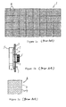
- FIG. 1a is a conventional LED display screen 1.
- the LED display screen 1 is an assembly of a plurality of LED display modules 2.
- Each display module 2 includes a rigid printed circuit board and integrated circuits.
- FIG. 1b is a cross sectional view of a conventional LED. It has components 5, 6 with pins 7 inserted through holes formed on the printed circuit board 3.
- LEDs are arranged into a LED matrix.
- the anodes and cathodes are connected together accordingly, and are then connected to external lead pins so as to facilitate the assembly of the LED display screen.
- FIG. 2a is a front view of a commercially available 8x8 LED display module 8 (2088AEG).
- FIG. 2b shows a circuit diagram of the 8x8 LED display module 8 of FIG. 2a .
- LED display screens are large, thick and heavy.
- a 1 m2 8x8 LED display module 8 (2088AEG) weighs about 24.6 Kg. Strong and heavy frames or supports are needed to support these LED display screens to ensure safety in the assembling process.
- the thickness of a conventional LED display screen is in the range of 5 cm and 50 cm. This kind of LED display screen is not suitable for installation in small space environments.
- the conventional LED display screens are rigid and not flexible. These conventional LED display screens are made of rigid PCB and can only be mounted on flat surfaces.
- LED display module is normally square in shape, and is limited in the choice of LED color and LED matrix. Longer delivery time and higher tooling expenses are incurred in order to produce customized LED display screen with special LED color, matrix and shape.
- conventional LED 4 as shown in FIG. 3 has a generally cylindrical housing 9 which obstructs the emission of LED light from the LED 4. LED light emits from a conventional LED at a narrow angle of about 110 degrees.
- a flexible LED screen includes a flexible printed circuit board having a front surface and a rear surface, a plurality of SMT-LEDs mounted on the front surface of the flexible printed circuit board, and a plurality of integrated circuits mounted on the rear surface of the flexible printed circuit board.
- the flexible printed circuit board may includes a base film having two opposite surfaces, two copper foils respectively adhered to the two opposite surfaces of the film base, and two coverlays respectively adhered to the two copper foils.
- the base film of the flexible printed circuit board may have a thickness ranging from about 0.0254 mm to about 0.0512 mm.
- the copper foil of the flexible printed circuit board may have a thickness ranging from about 0.01778 mm to about 0.07112 mm.
- the coverlay of the flexible printed circuit board may have a thickness ranging from about 0.0254 mm to about 0.0512 mm.
- the copper foils are adhered to the film base by an adhesive having a thickness ranging from about 0.01016 mm to about 0.0254 mm.
- the coverlays are adhered to the copper foils by an adhesive having a thickness ranging from about 0.0127 mm to about 0.03556 mm.
- the flexible LED screen may further include a front louver layer coupled to the front surface of the flexible printed circuit board.
- the front louver includes a plurality of openings sized and shaped to allow the SMT-LEDs to situate therein.
- the front louver layer may be made of silicon rubber or silicon dioxide and may have a thickness of about 2.8 mm.
- the flexible LED screen may further include a front foam layer sandwiched between the flexible printed circuit board and the front louver layer.
- the front foam layer may be made of silicon rubber and may have a thickness of about 3.5 mm.
- the flexible LED screen may further include a fixation layer coupled to a rear surface of the flexible printed circuit board to facilitate the fixing of the flexible LED screen to a support structure.
- the fixation layer includes a plurality of openings sized and shaped to allow the integrated circuits to situate therein.
- the fixation layer may be made of magnetic rubber and may have a thickness of about 1.5 mm.
- the flexible LED screen may further include a rear foam layer sandwiched between the flexible printed circuit board and the fixation layer.
- the rear foam layer may be made of silicon rubber and may have a thickness of about 3.5 mm.
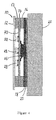
- FIG. 4 is a cross sectional view of the flexible LED screen 10 according to an embodiment disclosed in the present patent application.
- the flexible LED screen 10 includes a core layer 14, light emitting diodes (LEDs) 28, and integrated circuits 26.
- the flexible LED screen 10 may also includes a front louver layer 12, a front foam layer 17, a rear foam layer 16, and a fixation layer 18 for fixing the flexible LED screen 10 to an iron sheet 20 on a wall 22.
- the core layer 14 includes a flexible printed circuit (FPC) board 30 (as shown in Fig. 5 ) on which the LEDs 28 and the integrated circuits 26 are mounted.
- FPC flexible printed circuit
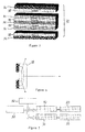
- FIG. 5 is an illustrative diagram depicting the flexible printed circuit board 30 of the flexible LED screen 10 according to an embodiment disclosed in the present patent application.
- the flexible printed circuit board 30 includes of a base film 32 having two opposite surfaces, two roll-pressed copper foils 34 respectively adhered to the two opposite surfaces of the film bas 32, and two coverlays 36 respectively adhered to the two copper foils 32.
- the base film 32 may be made of polymide (PI) or any suitable insulating materials. Polymide is known for its heat resistance and flame retardance characteristics. If heat resistance is not a concern, then polyester (PET) may be selected as the material for manufacturing the base film 32.
- the base film 32 may have a thickness ranging from about 0.0254 mm to about 0.0512 mm. Preferably, the base film 32 has a thickness of about 0.0381 mm.
- the two copper foils 34 are adhered on the two opposite surfaces of the base film 32 respectively by adhesive 38.
- the copper foils 34 may have a thickness ranging from about 0.01778 mm to about 0.0 7112 mm. Preferably, the copper foils 34 have a thickness of about 0.03556 mm.
- the copper foils 34 can pass a bending test of up to 10,000 times of bending without breaking.
- the copper foils 34 can be formed into electrical circuits by an etching process, and serve as electrical connections for electrical components of the flexible LED screen 10.
- Stiffeners made of the same material as the base film 32 may be formed on the base film 32 in the areas not covered by the copper foils 34 for stiffening purposes. It is understood that the stiffeners would not increase the thickness of the flexible printed circuit board 30.
- the adhesive 38 may be made of acrylic, expoxy resin, or any other suitable materials.
- the adhesive 38 may have a thickness ranging from about 0.01016 mm to about 0.0254 mm. Preferably, the adhesive 38 has a thickness of about 0.0254 mm.
- the two coverlays 36 may be made of polymide (PI), polyester (PET), or any other suitable materials.
- the coverlays 36 may have a thickness ranging from about 0.0254 mm to about 0,0512 mm. Preferably, the coverlays 36 has a thickness of about 0.0254 mm.
- the two coverlays 36 may be adhered on the two outer surfaces of the two adhered copper foils 34 respectively by adhesive 38.
- the adhesive 38 may be made of acrylic, expoxy resin, or any other suitable materials.
- the adhesive 38 for adhering the coverlays 36 to the copper foils 34 may have a thickness ranging from about 0.0127 mm to about 0.03556 mm. Preferably, the adhesive 38 has a thickness of about 0.0127 mm.
- the coverlays 36 cover the adhesive 38 and serve to protect the flexible printed circuit board 30.
- the thickness of the flexible printed circuit board 30 may be about 0.27 mm, which is much thinner than a conventional printed circuit board which usually has a thickness of about 1.6 mm.
- the flexible printed circuit board 30 has the same electrical properties and processability as the conventional printed circuit board.
- the flexible printed circuit board 30 is characterized in that it is thin, light-weight, and can be assembled into a three dimensional LED display structure.
- FIG. 6 is an illustrative diagram showing the transmission of light from a surface-mounting LED according to an embodiment disclosed in the present application.
- the LEDs 28 are mounted on the front surface of the flexible printed circuit board 30 by surface mount technology (SMT). This kind of LED is termed as SMT-LED.
- SMT-LED This kind of LED is termed as SMT-LED.
- the SMT-LED 28 may be a single basic color SMT-LED, or a double basic color SMT-LED, or a full color (3 colors) SMT-LED. These SMT-LEDs are much smaller in size and lighter in weight than conventional LEDs.
- the SMT-LEDs 28 are relatively flat and low profile as compared to conventional LEDs that have relatively large housings and elongated pins. This can greatly reduce the size and thickness of the Flexible LED screen 10.
- the SMT-LEDs 28 and the flexible printed circuit board 30 may have a total thickness of about 3 mm.
- a programmed machine is employed to pick and precisely place the SMT-LEDs 28 on the flexible printed circuit board 30.
- the flexible printed circuit board 30 is provided with solder pads that align with connections provided on the SMT-LEDs 28 to be mounted, and the programmed machine places the SMT-LEDs precisely over the solder pads during the manufacturing process. Once the SMT-LEDs 28 are placed in contact with the solder pads, heat is applied to the flexible printed circuit board 30 to a reflow temperature.
- a LED display with SMT-LEDs can produce a more uniform light intensity and a wider LED light angle than a LED screen with conventional LEDs, as illustrated in FIGS. 3 and 6 .
- the LED screen 10 of the present patent application can meet different customers' requirements on the layout, colors, shapes and configurations of a LED display screen by simply adjusting the flexible printed circuit board 30. According to the selection of SMT-LEDs, single basic color SMT-LED displays, double basic color SMT-LED displays, or full color SMT-LED displays can be produced.
- the LEDs 28 and the integrated circuits 26 are mounted on the front and rear surfaces of the flexible printed circuit board 30 respectively by surface mount technology.
- FIG. 7 is a block diagram showing the LED display screen system according to an embodiment disclosed in the present application.
- the LED display screen system includes the flexible printed circuit board 30, a signal processing unit 50 and a power supply unit 52.
- the power source from the power supply unit 52 may be AC-DC power source having an output voltage range between about +3.3V and about +15V.
- AC-DC power source having an output voltage range between about +3.3V and about +15V may be applied.
- the signal processing unit 50 serves as a control center of the LED screen 10. It records messages entered through computers, keyboards, remote controls, or wireless transmissions. The signal processing unit 50 converts the messages to digital signals, and then transmits the digital signals to the SMT-LEDs of the flexible printed circuit board 30 where the text messages, graphs, videos, etc. are displayed.
- the signal processing unit 50 may be in the form of a computer or a single chip microcomputer depending on the size of the data to be processed.
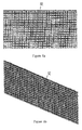
- FIGS. 8a and 8b are the front and perspective views respectively of the front louver layer 12 of the flexible LED display according to an embodiment disclosed in the present application.
- the front louver layer 12 may be made of silicon rubber, or silicon dioxide, or any other suitable materials.
- the front louver layer 12 may have a thickness of about 2.8 mm.
- the front louver layer 12 may be coupled to the LED-mounting side of the flexible printed circuit board 30, and serves to protect the flexible printed circuit board 30 and the SMT-LEDs 28.
- the front louver includes a plurality of openings sized and shaped to allow the SMT-LEDs to situate therein.
- the front louver layer 12 also gives the LED display a better outer appearance.
- FIG. 9 is a perspective view of the rear foam layer 16 of the flexible LED screen 10 according to an embodiment disclosed in the present application.
- the foam layer may be made of silicon rubber and may have a thickness of about 3.5 mm.
- the foam layer may be attached to the front and/or rear surfaces of the flexible printed circuit board 30 by adhesive means.
- the front louver layer 12 may then be attached to the front foam layer 17, as depicted in FIG. 4 .
- the rear foam layer 16, which is attached to the rear surface of the flexible printed circuit board 30, includes a plurality of openings sized and shaped to allow the integrated circuits to situate therein.
- the fixation layer 18 may then be attached to the rear foam layer 16, as depicted in FIG. 4 .
- the foam layer serves to protect the flexible printed circuit board 30.
- FIG. 10 is a perspective view of the fixation layer 18 of the flexible LED screen 10 according to an embodiment disclosed in the present application.
- the fixation layer 18 may be made of magnetic rubber and may have a thickness of about 1.5 mm.
- the fixation layer 18 includes a plurality of openings sized and shaped to allow the integrated circuits to situate therein.
- the fixation layer 18 serves to fix the flexible printed circuit board 30 on the wall 22 or any supporting structure.
- the wall 22 can be provided with an iron sheet 20.
- the flexible LED screen 10 can therefore be mounted on the wall 22 by the attractive magnetic force between the iron sheet 20 and the magnetic rubber fixation layer 18 of the flexible LED screen 10. Additional powerful magnets may be provided to ensure a more secured mounting of the flexible LED screen 10 on the wall 22.
- the flexible LED screen 10 may be mounted on the wall 22 by using hook-and-loop fasteners.
- the wall 22 can be provided with hook/loop fastener.
- the flexible LED screen 10 can therefore be mounted on the wall 22 by cooperating hook/loop fastener provided on the flexible LED screen 10.
- the flexible LED screen 10 so designed can remain thin, lightweight, and flexible. This makes installation of the flexible LED screen 10 easy and more efficient.
- the LED displays 10 can be mounted on surfaces like puzzles and can be completed by wiring up the flexible printed circuit board 30. To keep the flexible LED screen 10 as thin as possible, the signal processing unit 50 and the power supply unit 52 can be disposed external to the flexible LED screen 10.
- the flexible LED screen 10 including the front louver layer 12, the core layer 14, the foam layers 16 and 17, and the fixation layer 18, has a total thickness of less than 8 mm and a weight of less than 5kg/m 2 .
- a plurality of flexible LED screen 10 can be interconnected together physically and electrically to form flexible LED screens of different sizes and shapes.
- the flexible LED screen 10 may be mounted on flat or curve support surfaces to form a three dimensional LED display.
- the flexible LED screen 10 disclosed in the present patent application is flexible, thin, light-weight, easy to install, and provides a wider viewing angle.
- the flexible LED screen 10 may even expand its application in different industries such as textile, automobile, decoration, and toy industry.
Landscapes
- Engineering & Computer Science (AREA)
- Microelectronics & Electronic Packaging (AREA)
- Physics & Mathematics (AREA)
- General Physics & Mathematics (AREA)
- Theoretical Computer Science (AREA)
- Devices For Indicating Variable Information By Combining Individual Elements (AREA)
- Structure Of Printed Boards (AREA)
- Fastening Of Light Sources Or Lamp Holders (AREA)
- Led Device Packages (AREA)
- Illuminated Signs And Luminous Advertising (AREA)
Applications Claiming Priority (1)
| Application Number | Priority Date | Filing Date | Title |
|---|---|---|---|
| CNU2007201209607U CN201017568Y (zh) | 2007-06-22 | 2007-06-22 | 超薄柔性led显示屏系统 |
Publications (2)
| Publication Number | Publication Date |
|---|---|
| EP2023391A2 true EP2023391A2 (fr) | 2009-02-11 |
| EP2023391A3 EP2023391A3 (fr) | 2010-06-09 |
Family
ID=39058067
Family Applications (1)
| Application Number | Title | Priority Date | Filing Date |
|---|---|---|---|
| EP08158584A Withdrawn EP2023391A3 (fr) | 2007-06-22 | 2008-06-19 | Écran DEL flexible |
Country Status (3)
| Country | Link |
|---|---|
| US (2) | US9237652B2 (fr) |
| EP (1) | EP2023391A3 (fr) |
| CN (1) | CN201017568Y (fr) |
Cited By (3)
| Publication number | Priority date | Publication date | Assignee | Title |
|---|---|---|---|---|
| WO2016110483A1 (fr) | 2015-01-05 | 2016-07-14 | Barco N.V. | Affichage en mosaïque, mosaïque d'affichage et substrat de support pour utilisation dans ceux-ci |
| US10152914B2 (en) | 2013-10-28 | 2018-12-11 | Barco N.V. | Tiled display and method of assembling same |
| CN114822297A (zh) * | 2022-06-27 | 2022-07-29 | 深圳市宏贯光电科技有限公司 | 一种led显示屏软模组及其制作方法 |
Families Citing this family (25)
| Publication number | Priority date | Publication date | Assignee | Title |
|---|---|---|---|---|
| CN101582225B (zh) * | 2008-05-13 | 2013-03-20 | 蓝星光电科技股份有限公司 | 可挠式发光二极管显示屏 |
| CN201425819Y (zh) * | 2009-04-17 | 2010-03-17 | 袁钖鸿 | 一种柔性显示屏 |
| US20110148746A1 (en) * | 2009-12-18 | 2011-06-23 | Philip Eric Devorris | Sealed flexible light emitting diode display system with remote waterproof control |
| KR101381815B1 (ko) * | 2010-09-29 | 2014-04-07 | 삼성디스플레이 주식회사 | 터치 스크린 패널 및 그 제조방법 |
| CN102122463B (zh) * | 2011-03-24 | 2015-04-15 | 李海涛 | 一种贴片led显示屏的制造方法 |
| CN102724812A (zh) * | 2012-06-08 | 2012-10-10 | 王定锋 | 直接在软性线路板上焊接led制作的外露字和方法 |
| CN103400924B (zh) * | 2013-08-14 | 2015-11-25 | 中国科学院长春光学精密机械与物理研究所 | 微型柔性led阵列器件及制备方法 |
| US8976009B2 (en) | 2013-09-24 | 2015-03-10 | Peter McGie | Voice recognizing digital messageboard system and method |
| US20150110476A1 (en) * | 2013-10-22 | 2015-04-23 | Brian B. Walker | Low cost method of temporary in store product advertising for retail stores |
| USD786811S1 (en) * | 2015-09-15 | 2017-05-16 | Shenzhen coleder opto-electronics co, ltd | LED electronic display |
| US9734744B1 (en) * | 2016-04-27 | 2017-08-15 | Joan Mercior | Self-reacting message board |
| USD804712S1 (en) | 2016-05-23 | 2017-12-05 | Roe Visual Co., Ltd. | LED display screen with a quick installation structure |
| JP2017216272A (ja) * | 2016-05-30 | 2017-12-07 | 大日本印刷株式会社 | 多層回路基板及びそれを用いたledドットマトリックス表示装置 |
| CN106228912B (zh) * | 2016-07-29 | 2019-07-30 | 上海铁歌科技有限公司 | 一种可粘贴的超薄全彩led薄膜显示屏 |
| CN106912163A (zh) * | 2017-04-27 | 2017-06-30 | 福建祥云光电科技有限公司 | 小间距p2.5双层线路板制作工艺 |
| CN107180599B (zh) | 2017-05-12 | 2019-08-09 | Oppo广东移动通信有限公司 | 显示屏幕、显示装置和移动终端 |
| CN109424131A (zh) * | 2017-08-27 | 2019-03-05 | 南京乐朋电子科技有限公司 | 一种多功能超薄智能墙纸 |
| KR20200069125A (ko) * | 2018-12-06 | 2020-06-16 | 삼성전자주식회사 | 디스플레이 장치 |
| CN110364091A (zh) * | 2019-07-15 | 2019-10-22 | 深圳市广艺高科技有限公司 | 一种柔性led汽车广告屏及其制造方法 |
| US11452198B2 (en) * | 2019-07-25 | 2022-09-20 | Borgwarner, Inc. | Thermally insulated printed circuit board |
| CN111028708B (zh) * | 2019-12-16 | 2021-12-28 | 广州视源电子科技股份有限公司 | Led箱体及led显示屏 |
| CN113643653B (zh) * | 2021-08-12 | 2022-07-12 | 武汉华星光电技术有限公司 | 驱动电路、微发光二极管封装芯片及微发光二极管灯板 |
| CN114333652A (zh) * | 2022-01-17 | 2022-04-12 | 深圳市君同科技有限公司 | 一种柔性的led车载显示屏应用方法 |
| USD1090704S1 (en) * | 2022-12-05 | 2025-08-26 | Shenzhen TBD Optoelectronic Technology Co., Ltd. | Flexible LED screen |
| USD997112S1 (en) * | 2023-02-06 | 2023-08-29 | Shenzhen Biosled Technology Co., Ltd. | Flexible LED screen |
Family Cites Families (6)
| Publication number | Priority date | Publication date | Assignee | Title |
|---|---|---|---|---|
| US5949581A (en) * | 1997-08-12 | 1999-09-07 | Daktronics, Inc. | Display system |
| US6290713B1 (en) * | 1999-08-24 | 2001-09-18 | Thomas A. Russell | Flexible illuminators for phototherapy |
| US6811563B2 (en) * | 2003-01-09 | 2004-11-02 | Henry C. Savage, Jr. | Portable light delivery apparatus and methods for delivering light to the human body |
| WO2006052953A1 (fr) * | 2004-11-09 | 2006-05-18 | Steven Gardner | Dispositif et methode de phototherapie pour des nouveaux-nes presentant un ictere physiologique |
| JP2006186136A (ja) * | 2004-12-28 | 2006-07-13 | Toshiba Corp | 両面部品実装回路基板及びその製造方法 |
| TWI277381B (en) * | 2005-04-12 | 2007-03-21 | Au Optronics Corp | Double-sided flexible printed circuit board |
-
2007
- 2007-06-22 CN CNU2007201209607U patent/CN201017568Y/zh not_active Expired - Fee Related
-
2008
- 2008-06-19 EP EP08158584A patent/EP2023391A3/fr not_active Withdrawn
- 2008-06-20 US US12/142,778 patent/US9237652B2/en not_active Expired - Fee Related
-
2015
- 2015-12-02 US US14/957,593 patent/US9936561B2/en active Active
Cited By (6)
| Publication number | Priority date | Publication date | Assignee | Title |
|---|---|---|---|---|
| US10152914B2 (en) | 2013-10-28 | 2018-12-11 | Barco N.V. | Tiled display and method of assembling same |
| US10210794B2 (en) | 2013-10-28 | 2019-02-19 | Barco N.V. | Flexible display tile and method of producing same |
| US10600355B2 (en) | 2013-10-28 | 2020-03-24 | Barco N.V. | Tiled display and method of assembling same |
| WO2016110483A1 (fr) | 2015-01-05 | 2016-07-14 | Barco N.V. | Affichage en mosaïque, mosaïque d'affichage et substrat de support pour utilisation dans ceux-ci |
| US10114601B2 (en) | 2015-01-05 | 2018-10-30 | Barco N.V. | Tiled display, and display tile and carrier substrate for use in same |
| CN114822297A (zh) * | 2022-06-27 | 2022-07-29 | 深圳市宏贯光电科技有限公司 | 一种led显示屏软模组及其制作方法 |
Also Published As
| Publication number | Publication date |
|---|---|
| US9237652B2 (en) | 2016-01-12 |
| US20080316153A1 (en) | 2008-12-25 |
| US20160095183A1 (en) | 2016-03-31 |
| US9936561B2 (en) | 2018-04-03 |
| EP2023391A3 (fr) | 2010-06-09 |
| CN201017568Y (zh) | 2008-02-06 |
Similar Documents
| Publication | Publication Date | Title |
|---|---|---|
| US9936561B2 (en) | Flexible LED screen | |
| US7470055B2 (en) | Mounting structure for LED lighting systems | |
| JP5318853B2 (ja) | 光源装置及びそれを備えた表示装置 | |
| US6788541B1 (en) | LED matrix moldule | |
| US20070139929A1 (en) | Slim type backlight unit | |
| KR101266680B1 (ko) | 광원 장치 및 조명 장치 | |
| EP4071810B1 (fr) | Dispositif électronique | |
| KR101508991B1 (ko) | 전원부와 컨트롤러부가 설치되는 전광판프레임 결합 박스를 갖는 분리형 칩엘이디 전광판 시스템 | |
| CN215814923U (zh) | 显示模组和拼接显示装置 | |
| JP6333907B2 (ja) | 表示装置およびテレビジョン受信機 | |
| JPH06266299A (ja) | 表示装置 | |
| EP4290133A1 (fr) | Panneau d'éclairage à del léger | |
| CN102194384A (zh) | Led发光板及led显示屏 | |
| JP2018040852A (ja) | 表示装置およびテレビジョン受信機 | |
| JP2016033635A (ja) | 表示器 | |
| CN201753868U (zh) | 光源模块及具有该光源模块的显示装置 | |
| CN202307000U (zh) | Led发光板及led显示屏 | |
| CN212724549U (zh) | 一种低电磁辐射的led显示屏 | |
| KR101685390B1 (ko) | 슬림형 led모듈 및 그 슬림형 led모듈을 이용한 led 전광판 | |
| KR101833054B1 (ko) | 모듈형 투명 전광판 | |
| KR20120134172A (ko) | 엘이디 어셈블리 및 그를 포함하는 액정표시장치 | |
| JP2001117513A (ja) | 発光ダイオード表示装置 | |
| CN222233228U (zh) | Led灯板及具有其的led显示装置 | |
| KR102090525B1 (ko) | 플렉서블 투명 led 전광판 발광모듈 | |
| US20250120028A1 (en) | Display device |
Legal Events
| Date | Code | Title | Description |
|---|---|---|---|
| PUAI | Public reference made under article 153(3) epc to a published international application that has entered the european phase |
Free format text: ORIGINAL CODE: 0009012 |
|
| AK | Designated contracting states |
Kind code of ref document: A2 Designated state(s): AT BE BG CH CY CZ DE DK EE ES FI FR GB GR HR HU IE IS IT LI LT LU LV MC MT NL NO PL PT RO SE SI SK TR |
|
| AX | Request for extension of the european patent |
Extension state: AL BA MK RS |
|
| PUAL | Search report despatched |
Free format text: ORIGINAL CODE: 0009013 |
|
| AK | Designated contracting states |
Kind code of ref document: A3 Designated state(s): AT BE BG CH CY CZ DE DK EE ES FI FR GB GR HR HU IE IS IT LI LT LU LV MC MT NL NO PL PT RO SE SI SK TR |
|
| AX | Request for extension of the european patent |
Extension state: AL BA MK RS |
|
| 17P | Request for examination filed |
Effective date: 20101208 |
|
| AKX | Designation fees paid |
Designated state(s): AT BE BG CH CY CZ DE DK EE ES FI FR GB GR HR HU IE IS IT LI LT LU LV MC MT NL NO PL PT RO SE SI SK TR |
|
| 18D | Application deemed to be withdrawn |
Effective date: 20120103 |
|
| D18D | Application deemed to be withdrawn (deleted) | ||
| 17Q | First examination report despatched |
Effective date: 20151007 |
|
| STAA | Information on the status of an ep patent application or granted ep patent |
Free format text: STATUS: EXAMINATION IS IN PROGRESS |
|
| STAA | Information on the status of an ep patent application or granted ep patent |
Free format text: STATUS: THE APPLICATION IS DEEMED TO BE WITHDRAWN |
|
| R18D | Application deemed to be withdrawn (corrected) |
Effective date: 20180103 |