EP2023399A2 - Ein durch einen Strom aus Majoritätsträgern unterstützter Detektor für elektromagnetische Strahlung - Google Patents
Ein durch einen Strom aus Majoritätsträgern unterstützter Detektor für elektromagnetische Strahlung Download PDFInfo
- Publication number
- EP2023399A2 EP2023399A2 EP08167724A EP08167724A EP2023399A2 EP 2023399 A2 EP2023399 A2 EP 2023399A2 EP 08167724 A EP08167724 A EP 08167724A EP 08167724 A EP08167724 A EP 08167724A EP 2023399 A2 EP2023399 A2 EP 2023399A2
- Authority
- EP
- European Patent Office
- Prior art keywords
- current
- substrate
- majority
- detector
- mixer according
- Prior art date
- Legal status (The legal status is an assumption and is not a legal conclusion. Google has not performed a legal analysis and makes no representation as to the accuracy of the status listed.)
- Granted
Links
Images
Classifications
-
- H—ELECTRICITY
- H10—SEMICONDUCTOR DEVICES; ELECTRIC SOLID-STATE DEVICES NOT OTHERWISE PROVIDED FOR
- H10F—INORGANIC SEMICONDUCTOR DEVICES SENSITIVE TO INFRARED RADIATION, LIGHT, ELECTROMAGNETIC RADIATION OF SHORTER WAVELENGTH OR CORPUSCULAR RADIATION
- H10F77/00—Constructional details of devices covered by this subclass
- H10F77/10—Semiconductor bodies
- H10F77/14—Shape of semiconductor bodies; Shapes, relative sizes or dispositions of semiconductor regions within semiconductor bodies
-
- G—PHYSICS
- G01—MEASURING; TESTING
- G01S—RADIO DIRECTION-FINDING; RADIO NAVIGATION; DETERMINING DISTANCE OR VELOCITY BY USE OF RADIO WAVES; LOCATING OR PRESENCE-DETECTING BY USE OF THE REFLECTION OR RERADIATION OF RADIO WAVES; ANALOGOUS ARRANGEMENTS USING OTHER WAVES
- G01S7/00—Details of systems according to groups G01S13/00, G01S15/00, G01S17/00
- G01S7/48—Details of systems according to groups G01S13/00, G01S15/00, G01S17/00 of systems according to group G01S17/00
- G01S7/481—Constructional features, e.g. arrangements of optical elements
- G01S7/4816—Constructional features, e.g. arrangements of optical elements of receivers alone
-
- G—PHYSICS
- G01—MEASURING; TESTING
- G01S—RADIO DIRECTION-FINDING; RADIO NAVIGATION; DETERMINING DISTANCE OR VELOCITY BY USE OF RADIO WAVES; LOCATING OR PRESENCE-DETECTING BY USE OF THE REFLECTION OR RERADIATION OF RADIO WAVES; ANALOGOUS ARRANGEMENTS USING OTHER WAVES
- G01S7/00—Details of systems according to groups G01S13/00, G01S15/00, G01S17/00
- G01S7/48—Details of systems according to groups G01S13/00, G01S15/00, G01S17/00 of systems according to group G01S17/00
- G01S7/491—Details of non-pulse systems
- G01S7/4912—Receivers
- G01S7/4913—Circuits for detection, sampling, integration or read-out
-
- H—ELECTRICITY
- H10—SEMICONDUCTOR DEVICES; ELECTRIC SOLID-STATE DEVICES NOT OTHERWISE PROVIDED FOR
- H10F—INORGANIC SEMICONDUCTOR DEVICES SENSITIVE TO INFRARED RADIATION, LIGHT, ELECTROMAGNETIC RADIATION OF SHORTER WAVELENGTH OR CORPUSCULAR RADIATION
- H10F30/00—Individual radiation-sensitive semiconductor devices in which radiation controls the flow of current through the devices, e.g. photodetectors
- H10F30/20—Individual radiation-sensitive semiconductor devices in which radiation controls the flow of current through the devices, e.g. photodetectors the devices having potential barriers, e.g. phototransistors
- H10F30/21—Individual radiation-sensitive semiconductor devices in which radiation controls the flow of current through the devices, e.g. photodetectors the devices having potential barriers, e.g. phototransistors the devices being sensitive to infrared, visible or ultraviolet radiation
-
- G—PHYSICS
- G01—MEASURING; TESTING
- G01S—RADIO DIRECTION-FINDING; RADIO NAVIGATION; DETERMINING DISTANCE OR VELOCITY BY USE OF RADIO WAVES; LOCATING OR PRESENCE-DETECTING BY USE OF THE REFLECTION OR RERADIATION OF RADIO WAVES; ANALOGOUS ARRANGEMENTS USING OTHER WAVES
- G01S17/00—Systems using the reflection or reradiation of electromagnetic waves other than radio waves, e.g. lidar systems
- G01S17/88—Lidar systems specially adapted for specific applications
- G01S17/89—Lidar systems specially adapted for specific applications for mapping or imaging
- G01S17/894—Three-dimensional [3D] imaging with simultaneous measurement of time-of-flight at a two-dimensional [2D] array of receiver pixels, e.g. time-of-flight cameras or flash lidar
Definitions
- the present invention relates to the field of detection of electromagnetic radiation that generates minority carriers in a semi-conductor substrate, such as for example, but not limited to, detection of visible and infrared light More particularly, the present invention relates to electromagnetic radiation detection in a substrate and more specifically on the application of a majority current for directing photo-generated minority charges towards a detection region as well as an apparatus therefor.
- US-6157035 describes how a fast detector in a standard CMOS technology can be constructed.
- a shadow mask gives a spatial modulation to the incident, and consequently of the absorbed light in the semiconductor substrate.
- a fast detector is provided.
- Speed is hereby enhanced but the traded-off is sensitivity.
- WO 98/10255 and WO 99/60629 show methods and corresponding devices for determining the phase and/or amplitude of incident modulated light. These pixel structures are called photonic mixers. These structures are useful for making range-finding cameras giving depth or 3D information as is explained in these patent applications.
- the generated minority carriers in the substrate arrive preferentially at one of two detector accumulation zones.
- these accumulation zones are potential wells, created by a voltage on an adjacent accumulation gate.
- these accumulation zones are pn-junctions. There are however two major deficiencies with these photonic mixers.
- the generated minority carriers will have to diffuse towards the surface before the modulation photo-gates can redirect these carriers towards the destination accumulation zones. This diffusion process over a 5 to 20 ⁇ m distance limits the speed with which demodulation can be achieved. Second, the percentage of detected minority carriers that reach effectively the target accumulation zone is far from optimal.
- the present invention aims to provide a novel photo-detector structure that has a pn-junction detection area that can be of an order of magnitude smaller in area than the effective light sensitive area thereby lowering considerably the capacitance of the detecting pn-junction. Further, it is also an aim of the invention to provide a method of collecting photo-generated carriers that are present deeply in the substrate, in a fast way, in order to obtain a fast and sensitive detector.
- Another aim of the invention is to provide a photonic mixer structure and method that has two or more detector outputs, and whereby the photo-generated minority carriers get collected at a target detector output.
- An aim hereby is to reach this in a very efficient way, with high discrimination- and quantum efficiency. High detection bandwidth and high speed of switching between specified detector outputs are aimed for as well.
- the present invention provides a detector device for detection of electromagnetic radiation impinging on a substrate, the impinging electromagnetic radiation generating pairs of majority and minority carriers in the substrate.
- the detector device comprises means for generating, in the substrate, a majority carrier current, and at least one detection region for collecting generated minority carriers, the minority carriers being directed towards the at least one detection region under influence of the majority carrier current.
- the detector device may furthermore comprise at least one current source region and at least one current drain region, the means for generating the majority carrier current being adapted for generating this majority carrier current between the at least one current source region and the at least one current drain region.
- the at least one current source region may be located between the at least one current drain region and the at least one detection region.
- the at least one detection region may be located between the at least one current source region and the at least one current drain region.
- the current source region, the current drain region and the detection region may be located substantially in the same plane.
- substantially in the same plane is meant that they for example have a top surface in the same plane, as a plane is two-dimensional and per definition has no thickness, while the current source region, the current drain region and the detection region are three-dimensional structures.
- the current source region, current drain region and detection region may be located at the surface of the substrate of the detector device.
- the current source region may have an annular shape in the plane of the substrate. Also the current drain region may have an annular shape in the plane of the substrate.
- a detector device may furthermore comprise readout means for reading out the minority carriers collected in the detection region.
- the readout means may comprise a transimpedance amplifier.
- minority carriers having reached the at least one current source region may travel towards the at least one detection region by diffusion.
- the sensitive area of a detector according to the present invention may be substantially larger then the area of the at least one detection region.
- a detector device may be a photonic mixer.
- the means for generating the majority carrier current may be reconfigurable, so as to be able to generate the majority carrier current in either at least a first direction or a second direction different from the first direction.
- the second direction may be opposite to the first direction.
- the present invention provides the use of a detector according to the present invention in a time of flight range-finding application.
- the present invention provides a method for detection of electromagnetic radiation impinging on a substrate, the impinging electromagnetic radiation generating pairs of majority and minority carriers in the substrate.
- the method comprises generating a majority carrier current in the substrate, and directing generated minority carriers towards a detection region under influence of the generated majority carrier current.
- the method may furthermore comprise collecting the minority carriers in the detection region, and reading out the minority carriers collected in the detection region.
- a method according to the present invention may furthermore comprise generating the majority carrier current so as to at least first generate the majority carrier current in a first direction and to direct generated minority carriers towards a first detection region, and thereafter generate the majority carrier current in a second direction, the second direction being different with respect to the first direction, to thereby direct generated minority carriers towards a second detection region.
- the second direction may be opposite the first direction.
- a device A coupled to a device B should not be limited to devices or systems wherein an output of device A is directly connected to an input of device B. It means that there exists a path between an output of A and an input of B which may be a path including other devices or means.
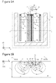
- Fig. 1A shows a top view of a first embodiment of a photo-detector according to the present invention.
- Sources 25 and 26 inject current at contacts 21 and 23 respectively, and drain current at contacts 20 and 24 respectively.
- Contacts 20, 21, 23 and 24 connect through ohmic-conduction to highly doped regions having a first conductivity type, e.g. p + -regions 12, 13, 14 and 15 respectively.
- a resistive, lightly doped substrate having the first conductivity type e.g. p- substrate 10
- a majority carrier current in the case of a substrate being a p- substrate, a hole current 19 will flow from region 13 to region 12, and from region 14 to region 15.
- FIG. 1A shows where the cross-section is made for Fig. 1B .
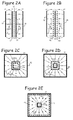
- the majority hole current 19 is shown by solid lines whereby the direction of the hole current 19 is indicated by arrows.
- the majority current 19 is associated with an electrical field, in the direction of the current. If incident electromagnetic radiation such as light in the form of a photon 16 is incident within a sensitive area 34 of the detector, the energy associated with the photon 16 is absorbed by the substrate 10, and a reaction takes place that generates an electron hole pair, at a certain position. In the example illustrated in Fig. 1B , the photon 16 falls into the right part of the sensitive area 34.
- Fig. 1B the majority hole current 19 is shown by solid lines whereby the direction of the hole current 19 is indicated by arrows.
- the majority current 19 is associated with an electrical field, in the direction of the current.
- the electron hole pair generation is considered to occur at the location indicated with a star: "*".
- the electron-hole pair e - /h + will be separated by the electrical field that is present and which is associated to the flowing majority hole current 19.
- the majority carrier of the electron-hole pair e - /h + in the present example the hole h + , will become indistinguishable from the sea of majority carriers, holes in this example, of the flowing majority hole current 19, and will follow for example trajectory 30.
- the minority carrier of the electron-hole pair namely in the example given the electron e - , on the contrary, will move in the opposite direction (due to its negative charge), driven by the same electrical field associated with the flowing majority current 19 and undergoes collisions with phonons, generating an erratic trajectory, like trajectory 29.
- This erratic trajectory 29 has however a general component that is opposite to the majority current flow 19 of the holes directing the electron e- towards the p + -region 14.
- the general component in the movement is due to drift based on the present electric field associated with the flowing majority current 19, and the erratic behaviour is due to diffusion, based on collisions with phonons.
- a detecting pn-junction 18 is provided.
- the minority carrier, electron e - being directed towards region 14, will have a large chance to reach the depletion zone of this junction 18, and to be detected due to its erratic behaviour (or diffusivity).
- the highly conductive region i.e. highly doped region having a second conductivity type, e.g. n + -region 17, through contact 22, connected to readout circuit 27.
- Readout circuit 27 is typically a transimpedance amplifier, and will typically be integrated on the same substrate 10 as the detector, thus avoiding packaging parasitics.
- the detecting pn-junction 18 is preferably located between a lowly doped well of the second conductivity type, n-well 33, and the substrate of the first conductivity type, p - -substrate 10.
- n + -region 17 is added inside the n-well 33 for making the detector finger formed by n + -region 17 and n-well 33 more conductive.
- junction capacitance per unit area is kept low, circuits attached to the photo-detector and optimised for this photo-detector with lower capacitance can reach a considerable better signal to noise output ratio and/or improved speed characteristics.
- the n-well 33 should be located close to the hole current sources 13 and 14 in order to increase the chance and the speed with which the electrons will diffuse into the n-well 33 through the detecting pn-junction 18, and thus to increase the sensitivity of the detector.
- Ohmic contacts in general serve as effective recombination centres for minority carriers, so ohmic contacts are preferably only present very locally, e.g. in a corner of p + -regions 13 and 14, like ohmic contacts 21 and 23 as illustrated in Fig. 1A .
- incident photons like photon 16 get absorbed in the substrate 10.
- the electrical field associated with the flowing majority current 19 will cause the photo-generated minority carriers (being electrons in the example given) to drift in the opposite direction to the flowing majority current 19, i.e. towards the source regions 14 and 13 of this majority current 19.
- the electrons arrive in the n + -region 17 and form the detector current going to the readout circuit 27.
- Beside photons like the example photon 16 a small fraction of the incident photons will be directly absorbed in the detecting finger 17 (region of n-well 33), not requiring the electric field associated to the majority current 19 for transportation.
- the region sensitive to incident photons becomes as large as region 34 illustrated in Fig. 1A and Fig. 1B , whilst the detecting finger 17 (region of n-well 33) has only a small capacitance due to its limited finger area. This can be an order of magnitude smaller than when the full sensitive area 34 would be covered with a pn-junction.
- This effect has similar benefits to focusing a wide incident light beam through a lens on a small area photo-detector.
- the large sensitive area 34 together with the small area pn-junction 18 for detection of the minority carriers effectively enhances the reachable signal to noise ratio.
- having a larger sensitive area 34 the alignment of light input means to the sensitive area will require less precision, lowering fabrication cost or connector precision (in the case of repeatable connections).
- the speed with which the electrons reach the detecting finger 17 depends on the magnitude of the electrical field that is associated with the majority hole current 19.
- a person skilled in the art can use device simulators (like ATLAS from Silvaco or MEDICI from Synopsys) and other calculation means or trial and error to determine which field has to be applied to reach a certain speed.
- a voltage of 2V gives for a trajectory distance of 20 ⁇ m, a delay of about 5 ns for movement of minority electrons in a silicon substrate 10. With a voltage of 2V and a 40 ⁇ m x 40 ⁇ m sensitive detector area, a speed of over 100 MHz can be obtained in standard CMOS.
- the required majority current 19 depends on the area, the distance between, and the width and length of regions 12, 13, 14 & 15.
- an assistant current of about 400 pA would flow with a 2 volt applied voltage at the sources 25 and 26.
- this assistant current can become very small.
- High resistive silicon substrates having a resistivity of 1000 ohm.cm are nowadays not uncommon, lowering the current down to even 8 ⁇ A, at roughly the same speed (since the electrical field distribution would remain more or less the same).
- the depth at which carriers still experience a reasonable field due to the majority current 19 is at about a 20 ⁇ m deep level D (in the Z direction - see Fig. 1 B) from the top of the substrate 10.
- D in the Z direction - see Fig. 1 B
- This increases the overall quantum efficiency of the detector, especially in cases where light is penetrating deeply in the substrate, like with light having a wavelength of 860 nm. In that case, electron-hole pair generation also occurs a depth of 20 microns.
- Standard CMOS technology typically only offers shallow junctions up to 2 microns deep. Light absorbed at 20 microns is difficult to capture for the junctions, since the generated minority carriers first have to diffuse to this shallow junction before getting detected and becoming part of a photo-current through the terminals of the detector.
- the readout circuit 27 may comprise a transimpedance amplifier.
- a transimpedance amplifier typically comprises an opamp 31 and a feedback resistor 32. It is used to convert an input current to an output voltage.
- the transimpedance amplifier 31, 32 can be designed to have about a 10 times higher transimpedance gain, when supposing that a ten times lower detector capacitance becomes feasible.
- the overall sensitivity i.e. the output voltage change at output node 28 of readout circuit 27 per unit incident light
- the signal to noise ratio improves as well, by a factor of 3 to 10, depending on whether the noise is mainly due to the noise of the input transistors in the transimpedance amplifier's amplifier 31 or due to the transimpedance amplifier's feedback resistor 32.
- Electromagnetic masking such as metal regions 11 can be used to prevent that the impinging electromagnetic radiation, such as light, penetrates in unwanted areas.
- Area 11 in Fig. 1A is an example of such an area.
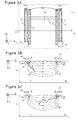
- Figs. 2A to 2E show several embodiments of devices according to the present invention.
- Fig. 2A shows a simplified diagrammatic top-view representation of the detector represented in Fig. 1A , whereby only the necessary subset of elements is represented.
- the thick solid lines represent the regions of the first conductivity type, p + -regions 12, 13, 14, 15, for applying the majority current.
- the thick dashed line represents the detector finger 17 in n-well region 33.
- the voltages applied by sources 25, 26 are also indicated.
- the voltage on the detector finger 17 is "Vdet". This voltage depends on how the transimpedance amplifier 31 is biased. Typically, this voltage is halfway the power supply voltage. For a power supply voltage of 5V, Vdet is thus typically 2.5V.
- Fig. 2B shows a second embodiment of a detector according to the present invention. It comprises only one source region 40 for injection of the majority current 19, with at each side of it a detector finger 41, 42. In the embodiment shown, the source region 40 is located in the middle of the device.
- the detector fingers 41, 42 should be connected in parallel. This set-up enhances the speed of the diffusion part of the detecting process, but it also doubles the detector capacitance, since the number of detector fingers 41, 42 is doubled.
- Fig. 2C and 2D illustrate detectors of a rectangular type.
- Fig. 2C is considered a preferred arrangement or best mode example, since in this embodiment the detector capacitance becomes extremely low.
- a detector finger 17 which for example has a dimension of 40 ⁇ m x 3 ⁇ m
- a current source region 43 which may be annular with a rectangular shape in top view, as illustrated in Fig. 2C , surrounds the detecting pn-junction 44.
- Current drain regions 45 are spaced apart for the current source region 43.
- the current drain regions 45 may also form an annular region with a rectangular shape in top view, as illustrated in Fig. 2C . Alternatively, not shown in the drawings, the current drain regions 45 do not need to touch each other, such that separated current drain regions 45 may be provided. In the same way, separated current source regions 43 may be provided around the detecting pn-junction 44.
- the detector of the third embodiment illustrated in Fig. 2D has in the centre its current source region 43, surrounded by a detecting pn-junction 44.
- the detector capacitance is somewhat higher, since the area of the detecting pn-junction 44 is somewhat larger, but it remains low. This set-up enhances the speed of the diffusion part of the detecting process, since the current source region 43 is surrounded by the detecting pn-junction 44.
- Fig. 2E shows a fifth embodiment of a detector according to the present invention, in which the minority carriers, e.g. electrons, are not driven to the centre, but to the edge of the detector.
- the current drain region 45 can be biased at a low, negative voltage, of e.g. -10V, without hindering the functioning of circuits outside the detector. This is preferred for higher speeds in the GHz range.
- the outside region(s) of the first conductivity type, e.g. a p + -ring 43 as in Fig. 2E or separated p + -regions, that sources the majority hole current 19 can be biased at a voltage higher than the negative voltage of the current drain region 45, at a high voltage, e.g. at 0V or 2V. With these stronger applied majority currents 19 and hence stronger electrical fields, up to GHz speeds can be obtained, still with a reasonably small detector capacitance.
- the structure of the device illustrated in Fig. 3 makes use of the same principles as the detector of Fig. 1 , however, it has another function.
- One of the uses is in "time of flight” (TOF) range-finding applications.
- TOF time of flight
- Prior art documents WO 98/10255 and WO 99/60629 explain the general principle of time of flight measurements for range finding applications.
- a light source is modulated at a frequency in the range of 1 MHz to 1 GHz. The light illuminates an object, or scene, and part of the reflected light enters the range finder camera through a focused lens.
- a distance can be estimated between the pixel and its conjugate (light-reflecting) pixel-area in the scene. In this way the distances of objects and the shape of objects can be estimated and recorded.
- Fig. 3A illustrates a photonic mixer according to an embodiment of the present invention, that mixes incident amplitude modulated electromagnetic radiation with an electrical signal applied to the substrate 10 through source 25, and outputs two electrical photo-currents at output nodes Mix1 and Mix2.
- Fig. 3B shows a cross-section through line III-III' of the device illustrated in Fig. 3A .
- the electrical signal applied by source 25, generates a majority current, e.g. majority hole current 19, through the substrate 10.
- Minority carriers like electrons in a p-substrate 10, will feel the electrical field that is associated with the applied majority hole current 19, and will drift towards a first source of majority carriers, e.g. holes, which is in the example illustrated p + -region 61. They will then diffuse into an adjacent first detection region, n-well 67, and they will become part of the output photocurrent of the left mixer connection point Mix1.
- a possible electron trajectory is trajectory 66, as illustrated in Fig. 3B .
- Electromagnetic masking such as metal areas 60, can be used to block unwanted light which otherwise would be directly incident on the detecting regions 67, 68.
- This photonic mixer has a high efficiency.
- the electrical field associated with the majority current 19, that cause the drift of the minority carriers, namely electrons, in the specified direction can penetrate deep in the substrate 10. How deep depends largely on the distance in X direction, i.e. parallel with the surface of the substrate 10, between p + -regions 61 and 62, as with the aforementioned detector of the present invention.
- a distance of 20 ⁇ m between regions 61 and 62 will accommodate light that penetrates about 20 ⁇ m deep.
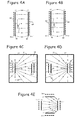
- Figs. 4A and 4B are simplified, schematic representations of the photonic mixer illustrated in Fig. 3A , for the two majority current conditions of Fig. 3B and 3C .
- the thick solid lines represent the p + -regions 61, 62 for applying the majority current 19.
- Thick dashed lines represent detector fingers 63, 64 in detection regions 67, 68. An example of applied voltages is also indicated.
- Figs. 4C and 4D represent a second embodiment of a photonic mixer according to the present invention, under two different majority current conditions.
- This mixer has further a current drain region, e.g. formed by a p + -ring or a plurality of separated p+-regions (not represented in the drawings), that surrounds the sensitive area 34, and that is always connected to a low voltage, e.g. GND (0V).
- a current drain region e.g. formed by a p + -ring or a plurality of separated p+-regions (not represented in the drawings)
- GND low voltage
- two short fingers 72, 73 of the first conductivity type, e.g. p + -fingers that are either connected to a high voltage, e.g. 2V, or disconnected (floating).
- the left short finger 72 is connected to the high voltage, e.g.
- phase estimation one would typically apply an electrical oscillating signal source 25 to the photonic mixer that is in phase, and thereafter (or in a second photonic mixer), one that is 90° delayed in phase with respect to the phase of the oscillating light source.
- an electrical oscillating signal source 25 For measuring the mixing products one would typically first reset the terminals Mix1 and Mix2 to a high voltage e.g. 5 Volt, and then apply the oscillating source 25 to the mixer, and after a measuring accumulation period, stop this oscillation for measuring what the integrated voltage drops on Mix1 and Mix2 have become. These voltage drops are then a result of the accumulation of the photo-current on nodes Mix1 and Mix2.
- Fig. 4E shows such a photonic mixer, having four current situations and four mixer outputs. More precise phase detection can be expected with this structure, since, 0, 90, 180 and 270 degrees mixing can be achieved during a same measuring accumulation period and on the same sensitive detector area.
- each p + -region is used as current inlet, e.g. by biasing it at a high voltage of e.g. 2V, whilst the other 3 p + -regions are kept at a low voltage of e.g. 0V. In that way, the direction of the majority current 19 in the middle of the mixer can be made to rotate in order to fulfil its mixing purpose.
- a person skilled in the art can also design other useful current configurations different from the one in Fig. 4E , without departing from the scope of the present invention.
- a current condition in which two or more p + -regions are simultaneously used as current inlet may be considered.
Landscapes
- Engineering & Computer Science (AREA)
- Computer Networks & Wireless Communication (AREA)
- Physics & Mathematics (AREA)
- General Physics & Mathematics (AREA)
- Radar, Positioning & Navigation (AREA)
- Remote Sensing (AREA)
- Light Receiving Elements (AREA)
- Photometry And Measurement Of Optical Pulse Characteristics (AREA)
- Measurement Of Radiation (AREA)
Priority Applications (1)
| Application Number | Priority Date | Filing Date | Title |
|---|---|---|---|
| EP08167724.7A EP2023399B1 (de) | 2003-09-02 | 2003-09-02 | Photomischdetektor |
Applications Claiming Priority (2)
| Application Number | Priority Date | Filing Date | Title |
|---|---|---|---|
| EP08167724.7A EP2023399B1 (de) | 2003-09-02 | 2003-09-02 | Photomischdetektor |
| EP03077744A EP1513202B1 (de) | 2003-09-02 | 2003-09-02 | Ein durch einen Strom aus Majoritätsträgern unterstützter Detektor für elektromagnetische Strahlung |
Related Parent Applications (1)
| Application Number | Title | Priority Date | Filing Date |
|---|---|---|---|
| EP03077744A Division EP1513202B1 (de) | 2003-09-02 | 2003-09-02 | Ein durch einen Strom aus Majoritätsträgern unterstützter Detektor für elektromagnetische Strahlung |
Publications (3)
| Publication Number | Publication Date |
|---|---|
| EP2023399A2 true EP2023399A2 (de) | 2009-02-11 |
| EP2023399A3 EP2023399A3 (de) | 2015-04-22 |
| EP2023399B1 EP2023399B1 (de) | 2020-01-08 |
Family
ID=34130237
Family Applications (2)
| Application Number | Title | Priority Date | Filing Date |
|---|---|---|---|
| EP03077744A Expired - Lifetime EP1513202B1 (de) | 2003-09-02 | 2003-09-02 | Ein durch einen Strom aus Majoritätsträgern unterstützter Detektor für elektromagnetische Strahlung |
| EP08167724.7A Expired - Lifetime EP2023399B1 (de) | 2003-09-02 | 2003-09-02 | Photomischdetektor |
Family Applications Before (1)
| Application Number | Title | Priority Date | Filing Date |
|---|---|---|---|
| EP03077744A Expired - Lifetime EP1513202B1 (de) | 2003-09-02 | 2003-09-02 | Ein durch einen Strom aus Majoritätsträgern unterstützter Detektor für elektromagnetische Strahlung |
Country Status (6)
| Country | Link |
|---|---|
| US (1) | US6987268B2 (de) |
| EP (2) | EP1513202B1 (de) |
| AT (1) | ATE456158T1 (de) |
| DE (1) | DE60331060D1 (de) |
| DK (1) | DK1513202T3 (de) |
| ES (1) | ES2339643T3 (de) |
Families Citing this family (52)
| Publication number | Priority date | Publication date | Assignee | Title |
|---|---|---|---|---|
| US20050038504A1 (en) * | 2003-01-22 | 2005-02-17 | Harry Halleriet | Kit for applying drug coating to a medical device in surgeon room |
| EP1665382B1 (de) * | 2003-09-18 | 2012-12-12 | iC-Haus GmbH | Optoelektronischer sensor und vorrichtung zur 3d-abstandsmessung |
| ITMI20062352A1 (it) * | 2006-12-06 | 2008-06-07 | Milano Politecnico | Struttura fotosensibile al colore di una radiazione luminosa |
| EP2081004A1 (de) * | 2008-01-17 | 2009-07-22 | Vrije Universiteit Brussel | Lichtspektrometer |
| US7615396B1 (en) * | 2008-04-28 | 2009-11-10 | Eugene Ching Lee | Photodiode stack for photo MOS relay using junction isolation technology |
| EP2116864A1 (de) | 2008-05-09 | 2009-11-11 | Vrije Universiteit Brussel | Entfernungsmessung mittels Laufzeitmessung mit Unterdrückung von Hintergrundstrahlung |
| WO2010144616A1 (en) | 2009-06-09 | 2010-12-16 | Mesa Imaging Ag | System for charge-domain electron subtraction in demodulation pixels and method therefor |
| GB2474631A (en) * | 2009-10-14 | 2011-04-27 | Optrima Nv | Photonic Mixer |
| JP5740413B2 (ja) | 2010-01-06 | 2015-06-24 | メサ・イメージング・アー・ゲーMesa Imaging Ag | ピクセルアレイと記憶アレイを別個に備える復調センサ |
| WO2011117161A2 (de) | 2010-03-26 | 2011-09-29 | Iee International Electronics & Engineering S.A. | Lichtsensor mit photoempfindlicher halbleiterstruktur |
| US9410800B1 (en) | 2010-08-02 | 2016-08-09 | Heptagon Micro Optics Pte. Ltd. | 3D TOF camera with masked illumination |
| GB2486208A (en) * | 2010-12-06 | 2012-06-13 | Melexis Tessenderlo Nv | Demodulation sensor and method for detection and demodulation of temporarily modulated electromagnetic fields for use in Time of Flight applications. |
| FR2977978A1 (fr) * | 2011-07-12 | 2013-01-18 | St Microelectronics Grenoble 2 | Dispositif de transfert de charges photogenerees haute frequence et applications |
| GB2492848A (en) | 2011-07-15 | 2013-01-16 | Softkinetic Sensors Nv | Optical distance measurement |
| US9140795B2 (en) | 2011-09-20 | 2015-09-22 | Mesa Imaging Ag | Time of flight sensor with subframe compression and method |
| DE102012109129B4 (de) | 2011-09-27 | 2017-06-29 | Heptagon Micro Optics Pte. Ltd. | Sensor-Pixelanordnung und getrennte Anordnung einer Speicherung und Akkumulation mit parallelem Erfassen und Auslesen |
| KR101696335B1 (ko) * | 2012-01-10 | 2017-01-13 | 소프트키네틱 센서스 엔브이 | 다중 스펙트럼 센서 |
| JP6246131B2 (ja) | 2012-01-10 | 2017-12-13 | ソフトキネティック センサーズ エヌブイ | タイムオブフライト信号の処理における又はこれに関する改良 |
| EP2703836B1 (de) | 2012-08-30 | 2015-06-24 | Softkinetic Sensors N.V. | TOF-Beleuchtungssystem und TOF-Kamera und Betriebsverfahren mit Steuerungsmitteln zur Ansteuerung der in der Szene vorhandenen elektronischen Vorrichtungen |
| DE102012109548B4 (de) * | 2012-10-08 | 2024-06-27 | pmdtechnologies ag | Auslesegate |
| JP5977366B2 (ja) * | 2013-01-10 | 2016-08-24 | ソフトキネティック センサー エヌブイ | カラー不可視光センサ、例えば、irセンサ、すなわち、マルチスペクトルセンサ |
| DE102013209161B4 (de) | 2013-05-16 | 2025-03-13 | pmdtechnologies ag | Lichtlaufzeitsensor |
| EP2894492B1 (de) | 2014-01-13 | 2020-10-28 | Sony Depthsensing Solutions SA/NV | Verfahren zur Ansteuerung eines Flugzeitsystems |
| EP2960952B1 (de) * | 2014-06-27 | 2019-01-02 | Sony Depthsensing Solutions SA/NV | Strahlungsdetektor mit Unterstützung durch einen Stromfluss von Majoritätsladungsträgern |
| TWI679442B (zh) | 2014-12-02 | 2019-12-11 | 新加坡商新加坡恒立私人有限公司 | 深度感測模組及深度感測方法 |
| GB201421512D0 (en) * | 2014-12-03 | 2015-01-14 | Melexis Technologies Nv | A semiconductor pixel unit for simultaneously sensing visible light and near-infrared light, and a semiconductor sensor comprising same |
| US10134926B2 (en) | 2015-02-03 | 2018-11-20 | Microsoft Technology Licensing, Llc | Quantum-efficiency-enhanced time-of-flight detector |
| TWI723890B (zh) | 2015-08-04 | 2021-04-01 | 光澄科技股份有限公司 | 製造影像感測陣列之方法 |
| EP3341970B1 (de) | 2015-08-27 | 2020-10-07 | Artilux Inc. | Optischer sensor mit breitem spektrum |
| US10886309B2 (en) | 2015-11-06 | 2021-01-05 | Artilux, Inc. | High-speed light sensing apparatus II |
| US10254389B2 (en) | 2015-11-06 | 2019-04-09 | Artilux Corporation | High-speed light sensing apparatus |
| US10739443B2 (en) | 2015-11-06 | 2020-08-11 | Artilux, Inc. | High-speed light sensing apparatus II |
| US10418407B2 (en) | 2015-11-06 | 2019-09-17 | Artilux, Inc. | High-speed light sensing apparatus III |
| EP3193190B1 (de) | 2016-01-15 | 2023-04-12 | Sony Depthsensing Solutions N.V. | Detektorvorrichtung mit majoritätsstrom und schaltung zur steuerung des stroms |
| EP3193369B1 (de) | 2016-01-15 | 2021-11-17 | Sony Depthsensing Solutions N.V. | Detektorvorrichtung mit majoritätsstrom und isoliermitteln |
| WO2017150391A1 (ja) * | 2016-03-04 | 2017-09-08 | ソニー株式会社 | 撮像装置及び測距システム |
| KR102391838B1 (ko) | 2016-06-20 | 2022-04-29 | 소니 세미컨덕터 솔루션즈 가부시키가이샤 | 드라이버 회로 및 전자 디바이스 |
| EP3497471B1 (de) | 2016-08-12 | 2021-11-24 | Sony Depthsensing Solutions | Demodulator mit einer ladungsträgererzeugenden gepinnten photodiode |
| BE1025050B1 (fr) | 2016-08-12 | 2018-10-12 | Softkinetic Sensors Nv | Démodulateur doté d’une photodiode pincée génératrice de porteurs et procédé de fonctionnement associé |
| WO2018206606A1 (en) | 2017-05-08 | 2018-11-15 | Vrije Universiteit Brussel | Detector for fast-gated detection of electromagnetic radiation |
| JP7167061B2 (ja) * | 2017-05-08 | 2022-11-08 | フリーイェ・ユニヴェルシテイト・ブリュッセル | 電磁放射線のファーストゲート式検出のための検出器 |
| US20200144436A1 (en) * | 2017-06-26 | 2020-05-07 | Sony Semiconductor Solutions Corporation | Single-photon avalanche diode and method for operating a single-photon avalanche diode |
| JP6761534B2 (ja) * | 2017-08-09 | 2020-09-23 | ソニーセミコンダクタソリューションズ株式会社 | 固体撮像装置、電子装置および固体撮像装置の制御方法 |
| JP7013448B2 (ja) | 2017-08-30 | 2022-01-31 | ソニーセミコンダクタソリューションズ株式会社 | 撮像素子および撮像装置 |
| US11105928B2 (en) | 2018-02-23 | 2021-08-31 | Artilux, Inc. | Light-sensing apparatus and light-sensing method thereof |
| US11482553B2 (en) | 2018-02-23 | 2022-10-25 | Artilux, Inc. | Photo-detecting apparatus with subpixels |
| US10886311B2 (en) | 2018-04-08 | 2021-01-05 | Artilux, Inc. | Photo-detecting apparatus |
| US11574942B2 (en) | 2018-12-12 | 2023-02-07 | Artilux, Inc. | Semiconductor device with low dark noise |
| CN114503265B (zh) | 2019-08-28 | 2023-05-23 | 光程研创股份有限公司 | 具有低暗电流的光侦测装置 |
| US12278252B2 (en) | 2019-08-28 | 2025-04-15 | Artilux, Inc. | Photo-detecting apparatus with low dark current |
| US12477856B2 (en) | 2019-08-28 | 2025-11-18 | Artilux, Inc. | Photo-detecting apparatus with low dark current |
| EP3907526B1 (de) | 2020-05-08 | 2024-03-13 | Melexis Technologies NV | Photonische mischvorrichtung |
Citations (3)
| Publication number | Priority date | Publication date | Assignee | Title |
|---|---|---|---|---|
| WO1998010255A1 (de) | 1996-09-05 | 1998-03-12 | Rudolf Schwarte | Verfahren und vorrichtung zur bestimmung der phasen- und/oder amplitudeninformation einer elektromagnetischen welle |
| WO1999060629A1 (de) | 1998-05-18 | 1999-11-25 | Rudolf Schwarte | Vorrichtung und verfahren zur erfassung von phase und amplitude elektromagnetischer wellen |
| US6157035A (en) | 1997-04-30 | 2000-12-05 | Imec | Spatially modulated detector for radiation |
Family Cites Families (5)
| Publication number | Priority date | Publication date | Assignee | Title |
|---|---|---|---|---|
| GB1548877A (en) * | 1975-06-26 | 1979-07-18 | Mullard Ltd | Semiconductor devices |
| EP0883187A1 (de) * | 1997-06-04 | 1998-12-09 | Interuniversitair Micro-Elektronica Centrum Vzw | Detektor für elektromagnetische Strahlung, Pixelstruktur mit höher Empfindlichkeit mit Verwendung dieses Detektors und Verfahren zu dessen Herstellung |
| BR0017356A (pt) * | 2000-10-16 | 2004-08-17 | Rudolf Schwarte | Processo e dispositivo para detectar e processar sinais de onda. |
| US6597025B2 (en) * | 2001-03-15 | 2003-07-22 | Koninklijke Philips Electronics N.V. | Light sensitive semiconductor component |
| US6515903B1 (en) * | 2002-01-16 | 2003-02-04 | Advanced Micro Devices, Inc. | Negative pump regulator using MOS capacitor |
-
2003
- 2003-09-02 AT AT03077744T patent/ATE456158T1/de not_active IP Right Cessation
- 2003-09-02 EP EP03077744A patent/EP1513202B1/de not_active Expired - Lifetime
- 2003-09-02 DK DK03077744.5T patent/DK1513202T3/da active
- 2003-09-02 DE DE60331060T patent/DE60331060D1/de not_active Expired - Lifetime
- 2003-09-02 EP EP08167724.7A patent/EP2023399B1/de not_active Expired - Lifetime
- 2003-09-02 ES ES03077744T patent/ES2339643T3/es not_active Expired - Lifetime
-
2004
- 2004-08-30 US US10/929,277 patent/US6987268B2/en not_active Expired - Lifetime
Patent Citations (3)
| Publication number | Priority date | Publication date | Assignee | Title |
|---|---|---|---|---|
| WO1998010255A1 (de) | 1996-09-05 | 1998-03-12 | Rudolf Schwarte | Verfahren und vorrichtung zur bestimmung der phasen- und/oder amplitudeninformation einer elektromagnetischen welle |
| US6157035A (en) | 1997-04-30 | 2000-12-05 | Imec | Spatially modulated detector for radiation |
| WO1999060629A1 (de) | 1998-05-18 | 1999-11-25 | Rudolf Schwarte | Vorrichtung und verfahren zur erfassung von phase und amplitude elektromagnetischer wellen |
Also Published As
| Publication number | Publication date |
|---|---|
| EP2023399B1 (de) | 2020-01-08 |
| US6987268B2 (en) | 2006-01-17 |
| DE60331060D1 (de) | 2010-03-11 |
| EP1513202B1 (de) | 2010-01-20 |
| EP2023399A3 (de) | 2015-04-22 |
| ES2339643T3 (es) | 2010-05-24 |
| US20050051730A1 (en) | 2005-03-10 |
| ATE456158T1 (de) | 2010-02-15 |
| DK1513202T3 (da) | 2010-05-10 |
| EP1513202A1 (de) | 2005-03-09 |
Similar Documents
| Publication | Publication Date | Title |
|---|---|---|
| EP2023399B1 (de) | Photomischdetektor | |
| JP6485880B2 (ja) | 多数電流によって補助される放射線検出器デバイス | |
| JP4814095B2 (ja) | 3次元距離測定用の光電子センサおよびデバイス | |
| US8294882B2 (en) | Photonic mixer and use thereof | |
| EP2284897B1 (de) | Demodulationspixel umfassender Majoritätsträgerstrom, eingegrabener Kanal und Hoch-Niedrig-Verbindung | |
| CN101688915B (zh) | 背面入射型测距传感器以及测距装置 | |
| KR102094738B1 (ko) | Pn-구조의 게이트 복조 화소 | |
| Ruegg | An optimized avalanche photodiode | |
| US20090224139A1 (en) | Drift Field Demodulation Pixel with Pinned Photo Diode | |
| Takeshita et al. | High-speed charge transfer pinned-photodiode for a CMOS time-of-flight range image sensor | |
| TW202001296A (zh) | 雪崩式之光電晶體 | |
| KR20200006083A (ko) | 전자기 방사선의 고속-게이트 검출을 위한 검출기 | |
| US7564022B1 (en) | Method and device for time-gating the sensitivity of an imager structure | |
| US20130221472A1 (en) | Range sensor and range image sensor | |
| CN112447875B (zh) | 雪崩式的光电晶体元件及其光检测方法 | |
| US9134423B2 (en) | Range sensor and range image sensor | |
| US7705285B2 (en) | Photodetector arrangement having a semiconductor body with plural layers and transistors, measurement arrangement with a photodetector arrangement and process for operating a measurement arrangement | |
| US11532663B2 (en) | Demodulator with a carrier generating pinned photodiode | |
| HK1128819A (en) | Detector for electromagnetic radiation assisted by majority current | |
| US7723668B2 (en) | Photodetector arrangement, measurement arrangement with a photodetector arrangement and process for operating a measurement arrangement | |
| Pancheri et al. | Current assisted photonic mixing devices fabricated on high resistivity silicon | |
| Hossain et al. | Current assisted photonic mixing demodulator implemented in 0.18 μm standard CMOS technology | |
| Pancheri et al. | A silicon metal-semiconductor-metal photodetector macromodel for circuit simulations | |
| Ripamonti et al. | Propagating avalanche position-sensitive photon detector with resolution in the micrometer and picosecond range | |
| Palojärvi et al. | Pn photodiodes for pulsed laser rangefinding applications realized in standard CMOS/BiCMOS processes |
Legal Events
| Date | Code | Title | Description |
|---|---|---|---|
| PUAI | Public reference made under article 153(3) epc to a published international application that has entered the european phase |
Free format text: ORIGINAL CODE: 0009012 |
|
| AC | Divisional application: reference to earlier application |
Ref document number: 1513202 Country of ref document: EP Kind code of ref document: P |
|
| AK | Designated contracting states |
Kind code of ref document: A2 Designated state(s): AT BE BG CH CY CZ DE DK EE ES FI FR GB GR HU IE IT LI LU MC NL PT RO SE SI SK TR |
|
| AX | Request for extension of the european patent |
Extension state: AL LT LV MK |
|
| REG | Reference to a national code |
Ref country code: HK Ref legal event code: DE Ref document number: 1128819 Country of ref document: HK |
|
| RIN1 | Information on inventor provided before grant (corrected) |
Inventor name: KUIJK, MAARTEN Inventor name: VAN NIEUWENHOVE, DANIEL |
|
| PUAL | Search report despatched |
Free format text: ORIGINAL CODE: 0009013 |
|
| AK | Designated contracting states |
Kind code of ref document: A3 Designated state(s): AT BE BG CH CY CZ DE DK EE ES FI FR GB GR HU IE IT LI LU MC NL PT RO SE SI SK TR |
|
| AX | Request for extension of the european patent |
Extension state: AL LT LV MK |
|
| RIC1 | Information provided on ipc code assigned before grant |
Ipc: G01J 1/42 20060101ALI20150313BHEP Ipc: H01L 31/0352 20060101AFI20150313BHEP |
|
| 17P | Request for examination filed |
Effective date: 20151022 |
|
| RBV | Designated contracting states (corrected) |
Designated state(s): AT BE BG CH CY CZ DE DK EE ES FI FR GB GR HU IE IT LI LU MC NL PT RO SE SI SK TR |
|
| AKX | Designation fees paid |
Designated state(s): AT BE BG CH CY CZ DE DK EE ES FI FR GB GR HU IE IT LI LU MC NL PT RO SE SI SK TR |
|
| AXX | Extension fees paid |
Extension state: LV Extension state: AL Extension state: LT Extension state: MK |
|
| STAA | Information on the status of an ep patent application or granted ep patent |
Free format text: STATUS: EXAMINATION IS IN PROGRESS |
|
| 17Q | First examination report despatched |
Effective date: 20190131 |
|
| GRAP | Despatch of communication of intention to grant a patent |
Free format text: ORIGINAL CODE: EPIDOSNIGR1 |
|
| STAA | Information on the status of an ep patent application or granted ep patent |
Free format text: STATUS: GRANT OF PATENT IS INTENDED |
|
| INTG | Intention to grant announced |
Effective date: 20190723 |
|
| GRAS | Grant fee paid |
Free format text: ORIGINAL CODE: EPIDOSNIGR3 |
|
| GRAA | (expected) grant |
Free format text: ORIGINAL CODE: 0009210 |
|
| STAA | Information on the status of an ep patent application or granted ep patent |
Free format text: STATUS: THE PATENT HAS BEEN GRANTED |
|
| AC | Divisional application: reference to earlier application |
Ref document number: 1513202 Country of ref document: EP Kind code of ref document: P |
|
| AK | Designated contracting states |
Kind code of ref document: B1 Designated state(s): AT BE BG CH CY CZ DE DK EE ES FI FR GB GR HU IE IT LI LU MC NL PT RO SE SI SK TR |
|
| RAP1 | Party data changed (applicant data changed or rights of an application transferred) |
Owner name: SONY DEPTHSENSING SOLUTIONS SA/NV |
|
| REG | Reference to a national code |
Ref country code: GB Ref legal event code: FG4D |
|
| REG | Reference to a national code |
Ref country code: CH Ref legal event code: EP |
|
| REG | Reference to a national code |
Ref country code: DE Ref legal event code: R096 Ref document number: 60352359 Country of ref document: DE |
|
| REG | Reference to a national code |
Ref country code: IE Ref legal event code: FG4D |
|
| REG | Reference to a national code |
Ref country code: AT Ref legal event code: REF Ref document number: 1223770 Country of ref document: AT Kind code of ref document: T Effective date: 20200215 |
|
| REG | Reference to a national code |
Ref country code: HK Ref legal event code: WD Ref document number: 1128819 Country of ref document: HK |
|
| REG | Reference to a national code |
Ref country code: NL Ref legal event code: MP Effective date: 20200108 |
|
| PG25 | Lapsed in a contracting state [announced via postgrant information from national office to epo] |
Ref country code: FI Free format text: LAPSE BECAUSE OF FAILURE TO SUBMIT A TRANSLATION OF THE DESCRIPTION OR TO PAY THE FEE WITHIN THE PRESCRIBED TIME-LIMIT Effective date: 20200108 Ref country code: PT Free format text: LAPSE BECAUSE OF FAILURE TO SUBMIT A TRANSLATION OF THE DESCRIPTION OR TO PAY THE FEE WITHIN THE PRESCRIBED TIME-LIMIT Effective date: 20200531 Ref country code: NL Free format text: LAPSE BECAUSE OF FAILURE TO SUBMIT A TRANSLATION OF THE DESCRIPTION OR TO PAY THE FEE WITHIN THE PRESCRIBED TIME-LIMIT Effective date: 20200108 |
|
| PG25 | Lapsed in a contracting state [announced via postgrant information from national office to epo] |
Ref country code: SE Free format text: LAPSE BECAUSE OF FAILURE TO SUBMIT A TRANSLATION OF THE DESCRIPTION OR TO PAY THE FEE WITHIN THE PRESCRIBED TIME-LIMIT Effective date: 20200108 Ref country code: GR Free format text: LAPSE BECAUSE OF FAILURE TO SUBMIT A TRANSLATION OF THE DESCRIPTION OR TO PAY THE FEE WITHIN THE PRESCRIBED TIME-LIMIT Effective date: 20200409 Ref country code: BG Free format text: LAPSE BECAUSE OF FAILURE TO SUBMIT A TRANSLATION OF THE DESCRIPTION OR TO PAY THE FEE WITHIN THE PRESCRIBED TIME-LIMIT Effective date: 20200408 |
|
| REG | Reference to a national code |
Ref country code: DE Ref legal event code: R097 Ref document number: 60352359 Country of ref document: DE |
|
| PG25 | Lapsed in a contracting state [announced via postgrant information from national office to epo] |
Ref country code: CZ Free format text: LAPSE BECAUSE OF FAILURE TO SUBMIT A TRANSLATION OF THE DESCRIPTION OR TO PAY THE FEE WITHIN THE PRESCRIBED TIME-LIMIT Effective date: 20200108 Ref country code: RO Free format text: LAPSE BECAUSE OF FAILURE TO SUBMIT A TRANSLATION OF THE DESCRIPTION OR TO PAY THE FEE WITHIN THE PRESCRIBED TIME-LIMIT Effective date: 20200108 Ref country code: SK Free format text: LAPSE BECAUSE OF FAILURE TO SUBMIT A TRANSLATION OF THE DESCRIPTION OR TO PAY THE FEE WITHIN THE PRESCRIBED TIME-LIMIT Effective date: 20200108 Ref country code: ES Free format text: LAPSE BECAUSE OF FAILURE TO SUBMIT A TRANSLATION OF THE DESCRIPTION OR TO PAY THE FEE WITHIN THE PRESCRIBED TIME-LIMIT Effective date: 20200108 Ref country code: EE Free format text: LAPSE BECAUSE OF FAILURE TO SUBMIT A TRANSLATION OF THE DESCRIPTION OR TO PAY THE FEE WITHIN THE PRESCRIBED TIME-LIMIT Effective date: 20200108 Ref country code: DK Free format text: LAPSE BECAUSE OF FAILURE TO SUBMIT A TRANSLATION OF THE DESCRIPTION OR TO PAY THE FEE WITHIN THE PRESCRIBED TIME-LIMIT Effective date: 20200108 |
|
| PGFP | Annual fee paid to national office [announced via postgrant information from national office to epo] |
Ref country code: FR Payment date: 20200914 Year of fee payment: 18 |
|
| PLBE | No opposition filed within time limit |
Free format text: ORIGINAL CODE: 0009261 |
|
| STAA | Information on the status of an ep patent application or granted ep patent |
Free format text: STATUS: NO OPPOSITION FILED WITHIN TIME LIMIT |
|
| REG | Reference to a national code |
Ref country code: AT Ref legal event code: MK05 Ref document number: 1223770 Country of ref document: AT Kind code of ref document: T Effective date: 20200108 |
|
| 26N | No opposition filed |
Effective date: 20201009 |
|
| PG25 | Lapsed in a contracting state [announced via postgrant information from national office to epo] |
Ref country code: IT Free format text: LAPSE BECAUSE OF FAILURE TO SUBMIT A TRANSLATION OF THE DESCRIPTION OR TO PAY THE FEE WITHIN THE PRESCRIBED TIME-LIMIT Effective date: 20200108 Ref country code: AT Free format text: LAPSE BECAUSE OF FAILURE TO SUBMIT A TRANSLATION OF THE DESCRIPTION OR TO PAY THE FEE WITHIN THE PRESCRIBED TIME-LIMIT Effective date: 20200108 |
|
| PG25 | Lapsed in a contracting state [announced via postgrant information from national office to epo] |
Ref country code: SI Free format text: LAPSE BECAUSE OF FAILURE TO SUBMIT A TRANSLATION OF THE DESCRIPTION OR TO PAY THE FEE WITHIN THE PRESCRIBED TIME-LIMIT Effective date: 20200108 |
|
| PG25 | Lapsed in a contracting state [announced via postgrant information from national office to epo] |
Ref country code: MC Free format text: LAPSE BECAUSE OF FAILURE TO SUBMIT A TRANSLATION OF THE DESCRIPTION OR TO PAY THE FEE WITHIN THE PRESCRIBED TIME-LIMIT Effective date: 20200108 |
|
| REG | Reference to a national code |
Ref country code: CH Ref legal event code: PL |
|
| REG | Reference to a national code |
Ref country code: BE Ref legal event code: MM Effective date: 20200930 |
|
| PG25 | Lapsed in a contracting state [announced via postgrant information from national office to epo] |
Ref country code: LU Free format text: LAPSE BECAUSE OF NON-PAYMENT OF DUE FEES Effective date: 20200902 |
|
| PG25 | Lapsed in a contracting state [announced via postgrant information from national office to epo] |
Ref country code: BE Free format text: LAPSE BECAUSE OF NON-PAYMENT OF DUE FEES Effective date: 20200930 Ref country code: CH Free format text: LAPSE BECAUSE OF NON-PAYMENT OF DUE FEES Effective date: 20200930 Ref country code: IE Free format text: LAPSE BECAUSE OF NON-PAYMENT OF DUE FEES Effective date: 20200902 Ref country code: LI Free format text: LAPSE BECAUSE OF NON-PAYMENT OF DUE FEES Effective date: 20200930 |
|
| REG | Reference to a national code |
Ref country code: GB Ref legal event code: 746 Effective date: 20210920 |
|
| PGFP | Annual fee paid to national office [announced via postgrant information from national office to epo] |
Ref country code: DE Payment date: 20210818 Year of fee payment: 19 Ref country code: GB Payment date: 20210820 Year of fee payment: 19 |
|
| PG25 | Lapsed in a contracting state [announced via postgrant information from national office to epo] |
Ref country code: TR Free format text: LAPSE BECAUSE OF FAILURE TO SUBMIT A TRANSLATION OF THE DESCRIPTION OR TO PAY THE FEE WITHIN THE PRESCRIBED TIME-LIMIT Effective date: 20200108 Ref country code: CY Free format text: LAPSE BECAUSE OF FAILURE TO SUBMIT A TRANSLATION OF THE DESCRIPTION OR TO PAY THE FEE WITHIN THE PRESCRIBED TIME-LIMIT Effective date: 20200108 |
|
| PG25 | Lapsed in a contracting state [announced via postgrant information from national office to epo] |
Ref country code: FR Free format text: LAPSE BECAUSE OF NON-PAYMENT OF DUE FEES Effective date: 20210930 |
|
| REG | Reference to a national code |
Ref country code: DE Ref legal event code: R119 Ref document number: 60352359 Country of ref document: DE |
|
| GBPC | Gb: european patent ceased through non-payment of renewal fee |
Effective date: 20220902 |
|
| PG25 | Lapsed in a contracting state [announced via postgrant information from national office to epo] |
Ref country code: DE Free format text: LAPSE BECAUSE OF NON-PAYMENT OF DUE FEES Effective date: 20230401 |
|
| PG25 | Lapsed in a contracting state [announced via postgrant information from national office to epo] |
Ref country code: GB Free format text: LAPSE BECAUSE OF NON-PAYMENT OF DUE FEES Effective date: 20220902 |