EP2028637A2 - Procédé d'affichage d'un appareil d'affichage d'émission - Google Patents
Procédé d'affichage d'un appareil d'affichage d'émission Download PDFInfo
- Publication number
- EP2028637A2 EP2028637A2 EP08162229A EP08162229A EP2028637A2 EP 2028637 A2 EP2028637 A2 EP 2028637A2 EP 08162229 A EP08162229 A EP 08162229A EP 08162229 A EP08162229 A EP 08162229A EP 2028637 A2 EP2028637 A2 EP 2028637A2
- Authority
- EP
- European Patent Office
- Prior art keywords
- display method
- display
- emission
- luminance
- pixel
- Prior art date
- Legal status (The legal status is an assumption and is not a legal conclusion. Google has not performed a legal analysis and makes no representation as to the accuracy of the status listed.)
- Withdrawn
Links
- 238000000034 method Methods 0.000 title claims abstract description 214
- 230000015556 catabolic process Effects 0.000 claims abstract description 110
- 238000006731 degradation reaction Methods 0.000 claims abstract description 109
- 235000019557 luminance Nutrition 0.000 description 176
- 238000010586 diagram Methods 0.000 description 29
- 230000000694 effects Effects 0.000 description 17
- 230000014509 gene expression Effects 0.000 description 16
- 239000003086 colorant Substances 0.000 description 14
- 230000007613 environmental effect Effects 0.000 description 9
- 238000012937 correction Methods 0.000 description 7
- 238000006243 chemical reaction Methods 0.000 description 6
- 238000005516 engineering process Methods 0.000 description 5
- 238000009499 grossing Methods 0.000 description 2
- 239000000463 material Substances 0.000 description 2
- 238000004364 calculation method Methods 0.000 description 1
- 239000012141 concentrate Substances 0.000 description 1
- 239000000470 constituent Substances 0.000 description 1
- 230000007547 defect Effects 0.000 description 1
- 238000010348 incorporation Methods 0.000 description 1
- 230000010354 integration Effects 0.000 description 1
- 238000004519 manufacturing process Methods 0.000 description 1
- 238000012986 modification Methods 0.000 description 1
- 230000004048 modification Effects 0.000 description 1
- 238000012545 processing Methods 0.000 description 1
- 230000002035 prolonged effect Effects 0.000 description 1
Images








Classifications
-
- G—PHYSICS
- G09—EDUCATION; CRYPTOGRAPHY; DISPLAY; ADVERTISING; SEALS
- G09G—ARRANGEMENTS OR CIRCUITS FOR CONTROL OF INDICATING DEVICES USING STATIC MEANS TO PRESENT VARIABLE INFORMATION
- G09G5/00—Control arrangements or circuits for visual indicators common to cathode-ray tube indicators and other visual indicators
- G09G5/02—Control arrangements or circuits for visual indicators common to cathode-ray tube indicators and other visual indicators characterised by the way in which colour is displayed
- G09G5/022—Control arrangements or circuits for visual indicators common to cathode-ray tube indicators and other visual indicators characterised by the way in which colour is displayed using memory planes
-
- G—PHYSICS
- G09—EDUCATION; CRYPTOGRAPHY; DISPLAY; ADVERTISING; SEALS
- G09G—ARRANGEMENTS OR CIRCUITS FOR CONTROL OF INDICATING DEVICES USING STATIC MEANS TO PRESENT VARIABLE INFORMATION
- G09G3/00—Control arrangements or circuits, of interest only in connection with visual indicators other than cathode-ray tubes
- G09G3/20—Control arrangements or circuits, of interest only in connection with visual indicators other than cathode-ray tubes for presentation of an assembly of a number of characters, e.g. a page, by composing the assembly by combination of individual elements arranged in a matrix no fixed position being assigned to or needed to be assigned to the individual characters or partial characters
- G09G3/22—Control arrangements or circuits, of interest only in connection with visual indicators other than cathode-ray tubes for presentation of an assembly of a number of characters, e.g. a page, by composing the assembly by combination of individual elements arranged in a matrix no fixed position being assigned to or needed to be assigned to the individual characters or partial characters using controlled light sources
- G09G3/30—Control arrangements or circuits, of interest only in connection with visual indicators other than cathode-ray tubes for presentation of an assembly of a number of characters, e.g. a page, by composing the assembly by combination of individual elements arranged in a matrix no fixed position being assigned to or needed to be assigned to the individual characters or partial characters using controlled light sources using electroluminescent panels
- G09G3/32—Control arrangements or circuits, of interest only in connection with visual indicators other than cathode-ray tubes for presentation of an assembly of a number of characters, e.g. a page, by composing the assembly by combination of individual elements arranged in a matrix no fixed position being assigned to or needed to be assigned to the individual characters or partial characters using controlled light sources using electroluminescent panels semiconductive, e.g. using light-emitting diodes [LED]
- G09G3/3208—Control arrangements or circuits, of interest only in connection with visual indicators other than cathode-ray tubes for presentation of an assembly of a number of characters, e.g. a page, by composing the assembly by combination of individual elements arranged in a matrix no fixed position being assigned to or needed to be assigned to the individual characters or partial characters using controlled light sources using electroluminescent panels semiconductive, e.g. using light-emitting diodes [LED] organic, e.g. using organic light-emitting diodes [OLED]
-
- G—PHYSICS
- G09—EDUCATION; CRYPTOGRAPHY; DISPLAY; ADVERTISING; SEALS
- G09G—ARRANGEMENTS OR CIRCUITS FOR CONTROL OF INDICATING DEVICES USING STATIC MEANS TO PRESENT VARIABLE INFORMATION
- G09G2320/00—Control of display operating conditions
- G09G2320/02—Improving the quality of display appearance
- G09G2320/0242—Compensation of deficiencies in the appearance of colours
-
- G—PHYSICS
- G09—EDUCATION; CRYPTOGRAPHY; DISPLAY; ADVERTISING; SEALS
- G09G—ARRANGEMENTS OR CIRCUITS FOR CONTROL OF INDICATING DEVICES USING STATIC MEANS TO PRESENT VARIABLE INFORMATION
- G09G2320/00—Control of display operating conditions
- G09G2320/02—Improving the quality of display appearance
- G09G2320/0257—Reduction of after-image effects
-
- G—PHYSICS
- G09—EDUCATION; CRYPTOGRAPHY; DISPLAY; ADVERTISING; SEALS
- G09G—ARRANGEMENTS OR CIRCUITS FOR CONTROL OF INDICATING DEVICES USING STATIC MEANS TO PRESENT VARIABLE INFORMATION
- G09G2320/00—Control of display operating conditions
- G09G2320/04—Maintaining the quality of display appearance
- G09G2320/043—Preventing or counteracting the effects of ageing
-
- G—PHYSICS
- G09—EDUCATION; CRYPTOGRAPHY; DISPLAY; ADVERTISING; SEALS
- G09G—ARRANGEMENTS OR CIRCUITS FOR CONTROL OF INDICATING DEVICES USING STATIC MEANS TO PRESENT VARIABLE INFORMATION
- G09G2320/00—Control of display operating conditions
- G09G2320/04—Maintaining the quality of display appearance
- G09G2320/043—Preventing or counteracting the effects of ageing
- G09G2320/046—Dealing with screen burn-in prevention or compensation of the effects thereof
-
- G—PHYSICS
- G09—EDUCATION; CRYPTOGRAPHY; DISPLAY; ADVERTISING; SEALS
- G09G—ARRANGEMENTS OR CIRCUITS FOR CONTROL OF INDICATING DEVICES USING STATIC MEANS TO PRESENT VARIABLE INFORMATION
- G09G2320/00—Control of display operating conditions
- G09G2320/04—Maintaining the quality of display appearance
- G09G2320/043—Preventing or counteracting the effects of ageing
- G09G2320/048—Preventing or counteracting the effects of ageing using evaluation of the usage time
-
- G—PHYSICS
- G09—EDUCATION; CRYPTOGRAPHY; DISPLAY; ADVERTISING; SEALS
- G09G—ARRANGEMENTS OR CIRCUITS FOR CONTROL OF INDICATING DEVICES USING STATIC MEANS TO PRESENT VARIABLE INFORMATION
- G09G2320/00—Control of display operating conditions
- G09G2320/06—Adjustment of display parameters
- G09G2320/0613—The adjustment depending on the type of the information to be displayed
-
- G—PHYSICS
- G09—EDUCATION; CRYPTOGRAPHY; DISPLAY; ADVERTISING; SEALS
- G09G—ARRANGEMENTS OR CIRCUITS FOR CONTROL OF INDICATING DEVICES USING STATIC MEANS TO PRESENT VARIABLE INFORMATION
- G09G2340/00—Aspects of display data processing
- G09G2340/04—Changes in size, position or resolution of an image
- G09G2340/0407—Resolution change, inclusive of the use of different resolutions for different screen areas
Definitions
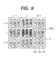
- FIG. 9 is a schematic diagram illustrating a pixel structure of the emission display apparatus used in the first embodiment of the present invention.
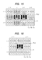
- FIG. 14 is a schematic diagram illustrating a pixel structure of the emission display apparatus used in the first embodiment of the present invention.
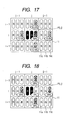
- FIG. 17 is a schematic diagram illustrating a pixel structure of the emission display apparatus used in the second embodiment of the present invention.
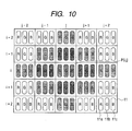
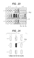
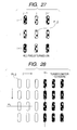
- FIGS. 1 to 15 are schematic diagrams each illustrating a pixel structure of an emission display apparatus used in a first embodiment of the present invention.
- ⁇ in the expressions indicates a luminance allocation (or distribution) ratio between the pixel P(i,j) and the nearby pixels.
- FIG. 30 is a block diagram illustrating a structure of the emission display apparatus according to an embodiment of the present invention.
- the emission display apparatus according to the embodiment of the present invention includes a signal input portion 1, a luminance distribution unit 2, an A/D conversion portion 3, and a display portion 4.
- the signal input portion 1 receives an image signal.
- the luminance distribution unit 2 performs luminance distribution processing on the image signal which is input to the signal input portion 1 and outputs the processed image signal to the A/D conversion portion 3.
- the A/D conversion portion 3 performs A/D conversion on the image signal which is output from the luminance distribution unit 2.
- the display portion 4 displays an image based on the image signal which is output from the A/D conversion portion 3.
- the emission display apparatus according to the embodiment of the present invention further includes a heat detecting portion 5 for detecting environmental temperature, a current detecting portion 6 for obtaining an emission luminance of the display portion 4, and an accumulated emission time measuring portion 7 for measuring an accumulated emission time.
- the emission luminance for the display color "a" of the pixel P(i,j) is represented by L a (i,j)
- the maximum emission luminance thereof is represented by L a MAX (i,j)
- the gradation thereof is represented by ⁇ a (i,j)
- the emission luminance L a (i,j) in the case where only the first display method is used for display can be expressed by Expressions (4), (5), and (6) below.
- the pixels of a region ⁇ i ⁇ ⁇ 2 ⁇ are allowed to emit light in a display mode in which the first display method is incorporated at a ratio of 1-4s and the second display method is incorporated at a ratio of 4s. That is, the pixel serving as the emission center emits light at a ratio of 1-4s and the current density is allocated (or distributed) at a ratio of s to each of nearby pixels located at upper, lower, right, and left positions.
Landscapes
- Engineering & Computer Science (AREA)
- Physics & Mathematics (AREA)
- Computer Hardware Design (AREA)
- General Physics & Mathematics (AREA)
- Theoretical Computer Science (AREA)
- Control Of Indicators Other Than Cathode Ray Tubes (AREA)
- Electroluminescent Light Sources (AREA)
- Control Of Gas Discharge Display Tubes (AREA)
Applications Claiming Priority (2)
| Application Number | Priority Date | Filing Date | Title |
|---|---|---|---|
| JP2007218370 | 2007-08-24 | ||
| JP2008189273A JP2009075563A (ja) | 2007-08-24 | 2008-07-23 | 発光表示装置の表示方法 |
Publications (2)
| Publication Number | Publication Date |
|---|---|
| EP2028637A2 true EP2028637A2 (fr) | 2009-02-25 |
| EP2028637A3 EP2028637A3 (fr) | 2010-07-21 |
Family
ID=39868195
Family Applications (1)
| Application Number | Title | Priority Date | Filing Date |
|---|---|---|---|
| EP08162229A Withdrawn EP2028637A3 (fr) | 2007-08-24 | 2008-08-12 | Procédé d'affichage d'un appareil d'affichage d'émission |
Country Status (2)
| Country | Link |
|---|---|
| US (2) | US8471787B2 (fr) |
| EP (1) | EP2028637A3 (fr) |
Cited By (4)
| Publication number | Priority date | Publication date | Assignee | Title |
|---|---|---|---|---|
| EP3016094A3 (fr) * | 2014-10-28 | 2016-08-03 | Samsung Display Co., Ltd. | Unité d'entrainement et dispositif d'affichage |
| EP3246908A4 (fr) * | 2015-01-15 | 2018-08-29 | Boe Technology Group Co. Ltd. | Procédé et dispositif de correction d'erreur de teinte de panneau d'affichage à delo et dispositif d'affichage |
| EP3754641A4 (fr) * | 2018-10-25 | 2021-11-24 | Shenzhen Skyworth-RGB Electronic Co., Ltd. | Procédé d'élimination d'images fantômes pendant un affichage amoled, terminal d'affichage, et support d'enregistrement |
| US11790843B2 (en) | 2020-05-01 | 2023-10-17 | Sony Group Corporation | Signal processing apparatus, signal processing method, and display apparatus |
Families Citing this family (22)
| Publication number | Priority date | Publication date | Assignee | Title |
|---|---|---|---|---|
| KR102031763B1 (ko) | 2013-01-11 | 2019-10-16 | 삼성디스플레이 주식회사 | 유기전계발광 표시장치 |
| JP2014240913A (ja) * | 2013-06-12 | 2014-12-25 | ソニー株式会社 | 表示装置および表示装置の駆動方法 |
| CN103700329B (zh) * | 2013-12-13 | 2015-11-11 | 北京京东方光电科技有限公司 | 显示面板的显示方法 |
| CN103824520B (zh) | 2014-01-26 | 2016-08-31 | 北京京东方光电科技有限公司 | 像素阵列及其驱动方法、显示面板和显示装置 |
| KR102194775B1 (ko) * | 2014-02-27 | 2020-12-24 | 삼성디스플레이 주식회사 | 영상 처리부, 이를 포함하는 표시 장치 및 이를 이용한 표시 패널 구동 방법 |
| TWI540566B (zh) * | 2014-12-09 | 2016-07-01 | 緯創資通股份有限公司 | 顯示器及其亮度、色彩補償方法與系統 |
| JP2016133590A (ja) * | 2015-01-19 | 2016-07-25 | ソニー株式会社 | 表示装置及び電子機器 |
| CN105046671B (zh) * | 2015-08-28 | 2017-12-22 | 厦门天马微电子有限公司 | 边缘处理方法及显示装置 |
| CN113192459A (zh) * | 2015-09-02 | 2021-07-30 | 天马微电子股份有限公司 | 显示装置 |
| CN106652899B (zh) * | 2015-10-29 | 2019-03-12 | 上海和辉光电有限公司 | 显示装置及显示面板的图像显示修正方法 |
| CN109003577B (zh) * | 2017-06-07 | 2020-05-12 | 京东方科技集团股份有限公司 | 显示面板的驱动方法及组件、显示装置、终端及存储介质 |
| KR102439146B1 (ko) * | 2017-09-26 | 2022-09-02 | 삼성전자주식회사 | 디스플레이 장치 및 그 제어방법 |
| JP2019095513A (ja) * | 2017-11-20 | 2019-06-20 | シナプティクス インコーポレイテッド | 表示ドライバ、表示装置及びサブピクセルレンダリング処理方法 |
| JP7292835B2 (ja) | 2018-08-22 | 2023-06-19 | 株式会社ジャパンディスプレイ | 表示装置 |
| KR102617392B1 (ko) * | 2019-02-20 | 2023-12-27 | 삼성디스플레이 주식회사 | 열화 보상 장치 및 이를 포함하는 표시 장치 |
| JP7225013B2 (ja) * | 2019-04-16 | 2023-02-20 | 株式会社ジャパンディスプレイ | 液晶表示装置 |
| CN110223642B (zh) * | 2019-05-31 | 2020-07-03 | 昆山国显光电有限公司 | 一种画面补偿方法和显示装置 |
| US11487125B2 (en) * | 2020-04-15 | 2022-11-01 | Google Llc | Laser safety in wearable heads-up displays |
| US11302289B2 (en) * | 2020-04-24 | 2022-04-12 | Rockwell Collins, Inc. | Display element, system, and method |
| WO2022145023A1 (fr) * | 2020-12-29 | 2022-07-07 | シャープ株式会社 | Dispositif d'affichage et procédé de pilotage de dispositif d'affichage |
| US11972713B2 (en) * | 2021-05-06 | 2024-04-30 | Apple Inc. | Systems and methods for point defect compensation |
| CN113745206B (zh) * | 2021-08-06 | 2024-06-18 | 武汉精测电子集团股份有限公司 | 一种led显示基板及其制作方法 |
Citations (4)
| Publication number | Priority date | Publication date | Assignee | Title |
|---|---|---|---|---|
| JP2000356981A (ja) | 1999-06-16 | 2000-12-26 | Mitsubishi Electric Corp | ディスプレイ表示制御装置 |
| JP2001175221A (ja) | 1999-12-17 | 2001-06-29 | Toshiba Corp | 表示装置 |
| US20030210256A1 (en) * | 2002-03-25 | 2003-11-13 | Yukio Mori | Display method and display apparatus |
| US20060132653A1 (en) * | 2004-12-16 | 2006-06-22 | Funai Electric Co., Ltd. | Video display device and video display method |
Family Cites Families (11)
| Publication number | Priority date | Publication date | Assignee | Title |
|---|---|---|---|---|
| US6724945B1 (en) | 2000-05-24 | 2004-04-20 | Hewlett-Packard Development Company, L.P. | Correcting defect pixels in a digital image |
| JP2002229505A (ja) * | 2001-01-31 | 2002-08-16 | Nec Corp | 表示装置 |
| JP3870807B2 (ja) * | 2001-12-20 | 2007-01-24 | ソニー株式会社 | 画像表示装置及びその製造方法 |
| EP1489589A4 (fr) * | 2002-03-04 | 2009-11-04 | Sanyo Electric Co | Affichage electroluminescent organique et son application |
| US20050179675A1 (en) * | 2002-05-27 | 2005-08-18 | Koninklijke Phillips Electonics N.C. | Pixel fault masking |
| US7822285B2 (en) | 2004-05-20 | 2010-10-26 | Omnivision Technologies, Inc. | Methods and systems for locally adaptive image processing filters |
| WO2006100906A1 (fr) * | 2005-03-18 | 2006-09-28 | Sharp Kabushiki Kaisha | Appareil et moniteur d'affichage d'image et televiseur |
| US7292024B2 (en) | 2005-04-28 | 2007-11-06 | Avago Technologies Ecbu Ip (Singapore) Pte Ltd | Defect mitigation in display panels |
| JP5110788B2 (ja) * | 2005-11-21 | 2012-12-26 | 株式会社ジャパンディスプレイイースト | 表示装置 |
| EP1990678A4 (fr) * | 2006-02-27 | 2010-08-25 | Sharp Kk | Affichage a cristaux liquides |
| JP2008116894A (ja) * | 2006-10-10 | 2008-05-22 | Pioneer Electronic Corp | ディスプレイパネルの駆動方法 |
-
2008
- 2008-08-04 US US12/185,347 patent/US8471787B2/en not_active Expired - Fee Related
- 2008-08-12 EP EP08162229A patent/EP2028637A3/fr not_active Withdrawn
-
2013
- 2013-05-16 US US13/895,550 patent/US20130229447A1/en not_active Abandoned
Patent Citations (4)
| Publication number | Priority date | Publication date | Assignee | Title |
|---|---|---|---|---|
| JP2000356981A (ja) | 1999-06-16 | 2000-12-26 | Mitsubishi Electric Corp | ディスプレイ表示制御装置 |
| JP2001175221A (ja) | 1999-12-17 | 2001-06-29 | Toshiba Corp | 表示装置 |
| US20030210256A1 (en) * | 2002-03-25 | 2003-11-13 | Yukio Mori | Display method and display apparatus |
| US20060132653A1 (en) * | 2004-12-16 | 2006-06-22 | Funai Electric Co., Ltd. | Video display device and video display method |
Cited By (7)
| Publication number | Priority date | Publication date | Assignee | Title |
|---|---|---|---|---|
| EP3016094A3 (fr) * | 2014-10-28 | 2016-08-03 | Samsung Display Co., Ltd. | Unité d'entrainement et dispositif d'affichage |
| US10255839B2 (en) | 2014-10-28 | 2019-04-09 | Samsung Display Co., Ltd. | Driving unit, display device and method of driving a display panel |
| EP3246908A4 (fr) * | 2015-01-15 | 2018-08-29 | Boe Technology Group Co. Ltd. | Procédé et dispositif de correction d'erreur de teinte de panneau d'affichage à delo et dispositif d'affichage |
| EP3754641A4 (fr) * | 2018-10-25 | 2021-11-24 | Shenzhen Skyworth-RGB Electronic Co., Ltd. | Procédé d'élimination d'images fantômes pendant un affichage amoled, terminal d'affichage, et support d'enregistrement |
| US11790843B2 (en) | 2020-05-01 | 2023-10-17 | Sony Group Corporation | Signal processing apparatus, signal processing method, and display apparatus |
| US12131692B2 (en) | 2020-05-01 | 2024-10-29 | Saturn Licensing Llc | Signal processing apparatus, signal processing method, and display apparatus |
| US12505792B2 (en) | 2020-05-01 | 2025-12-23 | Saturn Licensing Llc | Signal processing apparatus, signal processing method, and display apparatus |
Also Published As
| Publication number | Publication date |
|---|---|
| EP2028637A3 (fr) | 2010-07-21 |
| US20090051627A1 (en) | 2009-02-26 |
| US20130229447A1 (en) | 2013-09-05 |
| US8471787B2 (en) | 2013-06-25 |
Similar Documents
| Publication | Publication Date | Title |
|---|---|---|
| EP2028637A2 (fr) | Procédé d'affichage d'un appareil d'affichage d'émission | |
| KR100949942B1 (ko) | 발광표시장치의 표시방법 | |
| JP4966383B2 (ja) | 液晶表示装置 | |
| US10437546B2 (en) | Display apparatus and method of driving the same | |
| KR101134269B1 (ko) | 디스플레이 장치 및 디스플레이 장치의 휘도 조정 방법 | |
| EP3223266B1 (fr) | Dispositif d'affichage à diodes électroluminescentes organiques et son procédé de fonctionnement | |
| US20150302789A1 (en) | Display device, display panel driver and drive method of display panel | |
| US20080088548A1 (en) | Organic light emitting diode display device and driving method thereof | |
| KR20200029757A (ko) | 유기발광표시장치 | |
| KR20080101700A (ko) | 표시 장치, 표시 장치의 구동 방법 및 컴퓨터 프로그램 | |
| CN101923828A (zh) | 对显示器中的颜色偏移的补偿技术 | |
| KR20160026681A (ko) | 계조 검사 장치 및 계조 검사 방법 | |
| KR20160065397A (ko) | 표시 장치 및 그 구동 방법 | |
| US11908361B2 (en) | Display device and driving method therefor | |
| JP2010145810A (ja) | 表示装置 | |
| WO2017187565A1 (fr) | Dispositif d'affichage et procédé permettant de commander un dispositif d'affichage | |
| US20100188318A1 (en) | Display device | |
| CN101789211A (zh) | 影像显示装置 | |
| JP5680814B2 (ja) | 画像表示装置 | |
| CN113643660A (zh) | 显示装置以及显示装置的驱动方法 | |
| JP2009175415A (ja) | 液晶表示装置 | |
| US20230073431A1 (en) | System and method for reducing display artifacts | |
| JP2006243437A (ja) | ディスプレイ表示装置 | |
| KR20160082809A (ko) | 표시장치 | |
| CN116895252A (zh) | 显示面板及其驱动方法、驱动装置和亮度补偿方法 |
Legal Events
| Date | Code | Title | Description |
|---|---|---|---|
| PUAI | Public reference made under article 153(3) epc to a published international application that has entered the european phase |
Free format text: ORIGINAL CODE: 0009012 |
|
| AK | Designated contracting states |
Kind code of ref document: A2 Designated state(s): AT BE BG CH CY CZ DE DK EE ES FI FR GB GR HR HU IE IS IT LI LT LU LV MC MT NL NO PL PT RO SE SI SK TR |
|
| AX | Request for extension of the european patent |
Extension state: AL BA MK RS |
|
| PUAL | Search report despatched |
Free format text: ORIGINAL CODE: 0009013 |
|
| AK | Designated contracting states |
Kind code of ref document: A3 Designated state(s): AT BE BG CH CY CZ DE DK EE ES FI FR GB GR HR HU IE IS IT LI LT LU LV MC MT NL NO PL PT RO SE SI SK TR |
|
| AX | Request for extension of the european patent |
Extension state: AL BA MK RS |
|
| RIC1 | Information provided on ipc code assigned before grant |
Ipc: G09G 3/32 20060101ALI20100614BHEP Ipc: G09G 3/22 20060101AFI20081030BHEP |
|
| 17P | Request for examination filed |
Effective date: 20110121 |
|
| AKX | Designation fees paid |
Designated state(s): AT BE BG CH CY CZ DE DK EE ES FI FR GB GR HR HU IE IS IT LI LT LU LV MC MT NL NO PL PT RO SE SI SK TR |
|
| RIC1 | Information provided on ipc code assigned before grant |
Ipc: G09G 3/32 20060101ALI20110224BHEP Ipc: G09G 3/22 20060101AFI20110224BHEP |
|
| 17Q | First examination report despatched |
Effective date: 20110429 |
|
| STAA | Information on the status of an ep patent application or granted ep patent |
Free format text: STATUS: THE APPLICATION HAS BEEN WITHDRAWN |
|
| 18W | Application withdrawn |
Effective date: 20141006 |