EP2033295B1 - Einrichtung zum einspeisen einer ladung, einschliesslich integrierter energiespeicherung - Google Patents
Einrichtung zum einspeisen einer ladung, einschliesslich integrierter energiespeicherung Download PDFInfo
- Publication number
- EP2033295B1 EP2033295B1 EP07720181A EP07720181A EP2033295B1 EP 2033295 B1 EP2033295 B1 EP 2033295B1 EP 07720181 A EP07720181 A EP 07720181A EP 07720181 A EP07720181 A EP 07720181A EP 2033295 B1 EP2033295 B1 EP 2033295B1
- Authority
- EP
- European Patent Office
- Prior art keywords
- converters
- voltage
- power supply
- supply device
- converter
- Prior art date
- Legal status (The legal status is an assumption and is not a legal conclusion. Google has not performed a legal analysis and makes no representation as to the accuracy of the status listed.)
- Not-in-force
Links
Images
Classifications
-
- H—ELECTRICITY
- H02—GENERATION; CONVERSION OR DISTRIBUTION OF ELECTRIC POWER
- H02J—ELECTRIC POWER NETWORKS; CIRCUIT ARRANGEMENTS OR SYSTEMS FOR SUPPLYING OR DISTRIBUTING ELECTRIC POWER; SYSTEMS FOR STORING ELECTRIC ENERGY
- H02J7/00—Circuit arrangements for charging or discharging batteries or for supplying loads from batteries
- H02J7/34—Parallel operation in networks using both storage and other DC sources, e.g. providing buffering
- H02J7/345—Parallel operation in networks using both storage and other DC sources, e.g. providing buffering using capacitors as storage or buffering devices
-
- H—ELECTRICITY
- H02—GENERATION; CONVERSION OR DISTRIBUTION OF ELECTRIC POWER
- H02M—APPARATUS FOR CONVERSION BETWEEN AC AND AC, BETWEEN AC AND DC, OR BETWEEN DC AND DC, AND FOR USE WITH MAINS OR SIMILAR POWER SUPPLY SYSTEMS; CONVERSION OF DC OR AC INPUT POWER INTO SURGE OUTPUT POWER; CONTROL OR REGULATION THEREOF
- H02M1/00—Details of apparatus for conversion
- H02M1/0095—Hybrid converter topologies, e.g. NPC mixed with flying capacitor, thyristor converter mixed with MMC or charge pump mixed with buck
-
- H—ELECTRICITY
- H02—GENERATION; CONVERSION OR DISTRIBUTION OF ELECTRIC POWER
- H02M—APPARATUS FOR CONVERSION BETWEEN AC AND AC, BETWEEN AC AND DC, OR BETWEEN DC AND DC, AND FOR USE WITH MAINS OR SIMILAR POWER SUPPLY SYSTEMS; CONVERSION OF DC OR AC INPUT POWER INTO SURGE OUTPUT POWER; CONTROL OR REGULATION THEREOF
- H02M7/00—Conversion of AC power input into DC power output; Conversion of DC power input into AC power output
- H02M7/02—Conversion of AC power input into DC power output without possibility of reversal
- H02M7/04—Conversion of AC power input into DC power output without possibility of reversal by static converters
- H02M7/12—Conversion of AC power input into DC power output without possibility of reversal by static converters using discharge tubes with control electrode or semiconductor devices with control electrode
- H02M7/21—Conversion of AC power input into DC power output without possibility of reversal by static converters using discharge tubes with control electrode or semiconductor devices with control electrode using devices of a triode or transistor type requiring continuous application of a control signal
- H02M7/217—Conversion of AC power input into DC power output without possibility of reversal by static converters using discharge tubes with control electrode or semiconductor devices with control electrode using devices of a triode or transistor type requiring continuous application of a control signal using semiconductor devices only
-
- H—ELECTRICITY
- H02—GENERATION; CONVERSION OR DISTRIBUTION OF ELECTRIC POWER
- H02M—APPARATUS FOR CONVERSION BETWEEN AC AND AC, BETWEEN AC AND DC, OR BETWEEN DC AND DC, AND FOR USE WITH MAINS OR SIMILAR POWER SUPPLY SYSTEMS; CONVERSION OF DC OR AC INPUT POWER INTO SURGE OUTPUT POWER; CONTROL OR REGULATION THEREOF
- H02M7/00—Conversion of AC power input into DC power output; Conversion of DC power input into AC power output
- H02M7/42—Conversion of DC power input into AC power output without possibility of reversal
- H02M7/44—Conversion of DC power input into AC power output without possibility of reversal by static converters
- H02M7/48—Conversion of DC power input into AC power output without possibility of reversal by static converters using discharge tubes with control electrode or semiconductor devices with control electrode
- H02M7/483—Converters with outputs that each can have more than two voltages levels
- H02M7/4835—Converters with outputs that each can have more than two voltages levels comprising two or more cells, each including a switchable capacitor, the capacitors having a nominal charge voltage which corresponds to a given fraction of the input voltage, and the capacitors being selectively connected in series to determine the instantaneous output voltage
-
- H—ELECTRICITY
- H02—GENERATION; CONVERSION OR DISTRIBUTION OF ELECTRIC POWER
- H02M—APPARATUS FOR CONVERSION BETWEEN AC AND AC, BETWEEN AC AND DC, OR BETWEEN DC AND DC, AND FOR USE WITH MAINS OR SIMILAR POWER SUPPLY SYSTEMS; CONVERSION OF DC OR AC INPUT POWER INTO SURGE OUTPUT POWER; CONTROL OR REGULATION THEREOF
- H02M1/00—Details of apparatus for conversion
- H02M1/0067—Converter structures employing plural converter units, other than for parallel operation of the units on a single load
- H02M1/007—Plural converter units in cascade
-
- H—ELECTRICITY
- H02—GENERATION; CONVERSION OR DISTRIBUTION OF ELECTRIC POWER
- H02M—APPARATUS FOR CONVERSION BETWEEN AC AND AC, BETWEEN AC AND DC, OR BETWEEN DC AND DC, AND FOR USE WITH MAINS OR SIMILAR POWER SUPPLY SYSTEMS; CONVERSION OF DC OR AC INPUT POWER INTO SURGE OUTPUT POWER; CONTROL OR REGULATION THEREOF
- H02M1/00—Details of apparatus for conversion
- H02M1/0067—Converter structures employing plural converter units, other than for parallel operation of the units on a single load
- H02M1/0077—Plural converter units whose outputs are connected in series
-
- H—ELECTRICITY
- H02—GENERATION; CONVERSION OR DISTRIBUTION OF ELECTRIC POWER
- H02M—APPARATUS FOR CONVERSION BETWEEN AC AND AC, BETWEEN AC AND DC, OR BETWEEN DC AND DC, AND FOR USE WITH MAINS OR SIMILAR POWER SUPPLY SYSTEMS; CONVERSION OF DC OR AC INPUT POWER INTO SURGE OUTPUT POWER; CONTROL OR REGULATION THEREOF
- H02M7/00—Conversion of AC power input into DC power output; Conversion of DC power input into AC power output
- H02M7/42—Conversion of DC power input into AC power output without possibility of reversal
- H02M7/44—Conversion of DC power input into AC power output without possibility of reversal by static converters
- H02M7/48—Conversion of DC power input into AC power output without possibility of reversal by static converters using discharge tubes with control electrode or semiconductor devices with control electrode
- H02M7/483—Converters with outputs that each can have more than two voltages levels
- H02M7/487—Neutral point clamped inverters
Definitions
- the present invention relates to a device for powering a load, said power supply device comprising an integrated electrical power storage.
- Some consumers of electrical energy require on the one hand the supply of a determined electrical power, on the other hand the supply of a high energy during a relatively short period of the cycle. Such cycles can be repeated. Consumers of this type are, for example, the electromagnets of particle accelerators, the drive motors of rolling mills, the lifts and hoists, the cranes, etc. A direct coupling of such a consumer to the network electric can cause serious disturbances of said network. Means arranged between the power grid and the consumer are therefore generally responsible for storing energy in order to deliver it at the desired time, so that these consumption peaks are not directly provided by the network.
- the usual power supply devices are generally provided with resistive energy dissipators charged to dissipate energy when the power flow is reversed, which obviously wastes a lot of energy.
- energy storage means there are mechanical energy storage systems, for example the kinetic energy of a rotating flywheel, or electrostatic energy, for example in capacitors or supercapacitors, or magnetic energy, for example in chokes, or electrochemical energy, for example in storage batteries.
- mechanical energy storage systems for example the kinetic energy of a rotating flywheel, or electrostatic energy, for example in capacitors or supercapacitors, or magnetic energy, for example in chokes, or electrochemical energy, for example in storage batteries.
- the article "A Supercapacitor-Based Energy-Storage System for Elevators with Soft Commutated Interface” by A. Rufer, published in “IEEE Transactions on Industry Applications, Vol 38, No 5, September / October 2002 » describes an application of an elevator where the energy is used through the combination of a static converter and an electric drive machine.
- the static converter allows the continuous and bidirectional variation of the power flow from a DC intermediate circuit, itself powered by a rectifier circuit placed between this DC circuit and the AC primary network.
- the article describes a configuration further comprising drive portions, static converter and rectifier, a storage element, here a bank of supercapacitors connected to a DC link DC voltage. using an additional static converter.
- An object of the invention is therefore to propose a power supply device in which an energy storage element is placed directly at the DC intermediate circuit (s) without requiring the use of an additional static converter. .
- This firstly makes it possible to avoid back and forth flow of power in an additional converter, thus improving the energy efficiency of the supply device, which makes it possible to limit operating costs.
- Another object of the invention is to provide a bi-directional static converter device capable of supplying a consumer requiring high-level intermittent power requirements and for which the energy required is taken directly from the DC intermediate circuit or circuits.
- one of the aims of the invention is to propose a power supply device comprising a plurality of static converters connected in series and each comprising a capacitive intermediate circuit used as a storage element. In such a case, only a few of these converters are powered from the primary network.
- the other converters / storage units also have a capacitive intermediate circuit with DC voltage whose discharge and recharge are related to the power supply and the energy recovery of the coils of the magnets.
- another object of the invention is to propose a device for controlling and adjusting the operation of all the converters making it possible to transfer energy from one converter to the other during the circulation. of the delivered current, making it possible to maintain the average values of the voltages of the intermediate DC circuits by energy transfer of a converter to another, in particular from a converter powered to a non-powered converter.
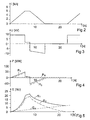
- the figure 2 schematically shows an exemplary form of a current pulse generally applied to the above consumer; the pulse first comprises a steady rise for about 0.65 s, followed by a plateau at about 6 kA for about 0.2 s and a steady descent, bringing the current back to zero, also for about 0.65 s. The pulse is repeated every 2.4 seconds or so.
- the form of the voltage pulse applied across the terminals of the set of coils of the synchrotron for applying the current pulse mentioned is represented in FIG. figure 3 ; from zero, the voltage rises abruptly to about 9 kV to remain stable throughout the duration of current rise of the coils; this voltage has a second plateau at about 2 kV during the current stage followed by a negative voltage sequence ranging from about -7.5 kV to about -10 kV during the current down, the voltage going back to zero for the end of the cycle .
- the figure 5 shows the shape of the curves representing the energy supplied to the load, these curves being obtained by integration into time function of the three curves of the previous figure.
- a first curve E T representing the total energy supplied to the load
- a second curve E M representing the energy supplied by the network
- the third curve E C represents the energy supplied by the storage device. It can be seen that this can reach values of the order of 20 MJ.
- This latter energy is supplied to the coils essentially during the period of rise of the current, a surplus being further provided during the current stage in order to compensate the losses, the coils then feeding the storage device during the decay of the current.
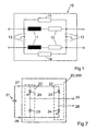
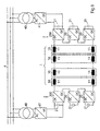
- the load 1 On the figure 6 showing a supply device according to the invention applied to the power supply of the CERN proton synchrotron, the load 1 consists of 101 coils 10 as described above with respect to FIG. figure 1 . Only 4 coils are shown in the figure , these being schematized only by their inductances 11, the other components of the equivalent diagram are not shown so as not to overload the figure. It can be seen in the figure that the load 1 is fed by its two opposite ends, which makes it possible to halve the supply voltage, by two sets of DC / DC converters 2, each set here comprising three cells 20, 200 mounted serial. The cells 200 are directly connected to the rectifier cells 41 while the cells 20 are not directly connected to said rectifier cells 41. The converters 2 are used as voltage variators, and as main storage elements of energy through their capacitors. continuous circuit 21.
- Each cell 20, 200 consists of a reversible chopper circuit comprising two branches 22 each comprising two elements, namely a diode 23 and an activatable and triggerable semiconductor element 24, for example a gate turn off thyristor (GTO) or IGCT (Integrated Gate Controlled Thyristor ) as shown in the figure or an IGBT transistor (Insulated Gate Bipolar Transistor), H-bridge mounted as in the figure.
- GTO gate turn off thyristor
- IGCT Integrated Gate Controlled Thyristor
- IGBT transistor Insulated Gate Bipolar Transistor
- the voltage transformation ratio ie the ratio between the average value of the output voltage between the terminals 25 and 26 and the input voltage between the terminals 27 and 28, ie the voltage across the capacitor 21, can be controlled for each cell 20, 200 of DC / DC converter by a modulation circuit for switching on and off the semiconductors 24 in variable durations as described below.
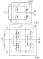
- FIGS. Figures 8 and 9 Other embodiments of DC / DC converter cells 20, 200 are shown in FIGS. Figures 8 and 9 .
- inverter branches of known technology are used, according to standardized executions from industrial applications.
- the branches 22 are then constituted of so-called “two-level” inverters, as shown in FIG. figure 8 or "at three levels", as represented on the figure 9 .
- the storage capacitor 21 associated with such a cell 20, 200 is replaced by two capacitors in series. Additional components such as switching assistance circuits, inductors, capacitors, resistors or the like may be included in such circuits; they were not represented in the figures so as not to overload them.
- the DC / DC converters 20, 200 may comprise several branches 20 connected in parallel.
- the number of cells 20, 200 of DC / DC converters depends essentially on the application in question; and more particularly the level of voltage that it is necessary to achieve with respect to the maximum voltage that can withstand a capacitor.
- the CERN proton synchrotron power supply six cells 20, 200 in series are provided, divided into two groups of three as on the figure 6 . So, for a maximum total voltage applied to the 9 kV load as on the figure 2 this voltage is divided by six according to the number of cells 20, 200, thus giving an average voltage of the order of 1.5 kV across each cell 20, 200 respectively at the terminals of each capacitor 21.
- the operation of the cells 20 and 200 of the DC / DC converters is done according to the principle of pulse duration modulation (PWM) with a pulse frequency (chopper frequency) in constant general.
- PWM pulse duration modulation
- the latching and tripping control signals of the power semiconductors 24 are generated by modulators as explained below.
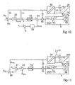
- FIG. figure 10 An embodiment of a pulse duration modulator (PWM) 5 coupled to a DC / DC converter cell 20 not directly connected to a rectifier cell 41 is shown in FIG. figure 10 .
- PWM pulse duration modulator
- the voltages U k1 to U k n measured at the terminals of all the capacitors 21 by the measuring instrument 56 are first summed and then a mean value U moy is drawn from it in the element 50. This value U av is then compared. in a comparator 51 at the voltage U k measured across the capacitor 21 corresponding to the controlled cell 20. Via a P / PI corrector 52, a duty cycle portion is added or subtracted, by a comparator 53, to a main duty cycle provided by a state regulator 54, calculating said main duty cycle from the current value to provide load and X state values measured on the load. The comparator 53 thus provides a reference voltage U cm0 . This is introduced into a divider 54 which also receives a voltage proportional to the voltage U k measured across the capacitor 21.
- the resulting signal is introduced into a discriminator 55 delivering a binary signal S k sent as the control signal of each of the semiconductors engageable and releasable 24, respectively on the GTO thyristor gates or the bases of the IGBT transistors mounted in the DC / DC converter cell 20.
- the capacitor 21 discharges, therefore, it is possible to carry out a voltage correction by performing a division of U cm by a signal proportional to U d .
- Each of said DC / DC converter cells 20 is controlled by a modulator 5 as described above.
- the cells 200 of the DC / DC converters directly connected to the rectifier cells 41 are controlled by a power adjustment making it possible to ensure that said cells 200 provide the desired power, able to compensate for losses in the supply device as well as in load.
- a proportion of the resulting signal is then added, using the adder 61, to a value P c representing an ideal power setpoint calculated from a model of the system which makes it possible to determine the loss power at each instant according to of the value of the current flowing in the magnets 10. If the losses are exactly compensated, the value U moy just before the cycle is identical to the reference value U ref and the capacitors 21 are fully loaded.
- a correction, given by the comparator 60, is introduced only if these values are different, so as to maintain the voltages of the capacitors 21 at their reference voltage.
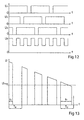
- each can be controlled by modulators generating control signals S k which are not in phase but which are offset with each other in order to obtain an output voltage supplied to the coils 10 of which The ripple is reduced compared to an operation where all the cells would be controlled by in-phase signals.
- An example of output voltages is shown at the figure 12 . It shows the voltages U 1 , U 2 and U 3 at the terminals 25, 26 of the cells 20 and whose amplitude variation is 100% for each.
- the voltage U T which represents the sum of the voltages of the cells, ie the voltage across the load 1 has only a variation of amplitude of 33%. At the same time, its pulse frequency has risen sharply.
- Each cell 20, 200 of DC / DC converter is connected in series to its neighbor by its output terminals 25, 26.
- each DC / DC converter cell 20, 200 between the terminals 25 and 26 depends on the value of the voltage of the capacitor 21 associated therewith.
- a control device is necessary to correct the modulation rate of each cell 20, 200 as a function of the supply voltage of the capacitor 21.
- the figure 13 schematically shows the principle of capacitor discharge correction by increasing the duty cycle of the modulator. At the beginning of the discharge, on the left side of the figure, the duty cycle is about 50%; whereas when the capacitor 21 is discharged, or on the right side of the figure, the same duty cycle is about 90%.
- each DC / DC converter cell 20, 200 between the terminals 25 and 26 depends on the value of the voltage of the capacitor 21 associated therewith. This voltage variation is reflected in the total voltage supplied to the coils 10 by putting the cells 20, 200 of the DC / DC converter in series.
- the charge and discharge cycles of the coils 10 described above cause losses in the various circuit components.
- energy is taken from the electrical network 4 (see figure 6
- the DC / DC converters 2 are connected to the electrical network 4 via transformers 40 and rectifier cells 41, feeding two cells 200 of DC / DC converters.
- the transformers 40 serve only to obtain an acceptable voltage level at the input of the rectifier cells 41 and to galvanically isolate the load from the network.
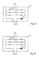
- the rectifier cells 41 consist of a diode bridge 42 as shown in FIG. figure 14 .
- the lack of control of the diode rectifiers 42 does not change the voltage across the capacitors 21 of the cells 200 of the DC / DC converters.
- Such a device therefore does not make it possible to use the energy accumulated in the capacitors 21 directly connected to said cells 200 of the DC / DC converters connected to the rectifier cells 41.
- a smoothing choke 43 is provided at the positive output of the bridge.
- the variation of the output voltage of the rectifier cells 41 remains possible given the pulsation principle of the cells 200 of the DC / DC converters described above.
- the energy contribution of the capacitors 21 of the cells 200 of the DC / DC converters directly powered by the rectifier cells 41 the two cells 200 of the top in the diagram of the figure 6 is therefore zero and the power transmitted can only be provided by the rectifier cells 41, respectively by the network.
- the capacitors 21 of the cells 20 of the DC / DC converters not directly connected to the rectifier cells 41, the four cells of the bottom in the diagram of the figure 6 operate as storage elements.
- rectifier cells 41 similar to one of the two following embodiments will be chosen, thus allowing the set of capacitors 21 of the cells 20 of the DC / DC converters to function as storage elements.
- the rectifier cells 41 consist of a thyristor bridge 44 as shown in FIG. figure 15 .
- the ignition angle ⁇ of the thyristors 44 will be varied as a function of the variation of the voltage. This voltage variation therefore allows the energy discharge of the capacitors 21.
- the instantaneous power supplied by the thyristor rectifier cells 41 is thus not equal to the instantaneous power transmitted to the load.
- a smoothing choke 43 is provided at the positive output of the cell 41.
- thyristors in the rectifier cells 41 with a control of the ignition angle ⁇ of said thyristors 44, implies a variation of the phase shift angle between the voltage and the alternating current at the input of the rectifiers 41, thereby causing a reactive power consumption to the primary network.
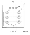
- the rectifier cells 41 consist of pulse rectifiers as shown in FIG. figure 16 .
- the rectifier cell 41 comprises a bridge circuit consisting of thyristors 45 of the GTO or IGCT type, as shown in the left-hand portion of the figure, or transistors 46, of the IGBT type, as represented on the portion of FIG. right of the figure, it being understood that the bridge consists solely of semiconductor elements of one or the other type.
- Each of said above semiconductor elements 45 or 46 comprises a diode 47 mounted in antiparallel.
- the connections to the AC primary electrical network must be made via decoupling and smoothing inductors 48 as shown in the figure.
- Another advantage of such an arrangement lies in the fact that it is possible to freely impose the fundamental phase shift of the current, thus making it possible to impose a cos ⁇ , or even to operate with a unit cos ⁇ or even use these rectifier cells as reactive power compensators if necessary.
- a pulsed rectifier cell 41 as described herein imposes a lower limit of the output voltage supplied to the capacitors 21, this voltage not being less than the peak value of the input AC voltage of the cell 41. case where this DC voltage would become lower than this peak value only the diodes 47 would remain active, even in the case where thyristors 45 or transistors 46 would not be activated.
- the rectifier cell 41 would then operate as a diode rectifier, uncontrollable.
- the output of the DC side has a minimum capacitance C int , marked 49 in the figure.
- the capacitors 21 are relatively close to the cells of the pulse rectifiers 41, they can act as an output capacitance of said cells.
- a power supply device capable of delivering a relatively low value average power accompanied by power peaks provided by storage means integrated with said power supply device.
- circuits, components, semiconductor elements or cell numbers may be different as described above, depending on the type of load encountered or the current pulse to be supplied, but without departing from the the scope of the claims.
Landscapes
- Engineering & Computer Science (AREA)
- Power Engineering (AREA)
- Dc-Dc Converters (AREA)
- Charge And Discharge Circuits For Batteries Or The Like (AREA)
- Rectifiers (AREA)
- Emergency Protection Circuit Devices (AREA)
- Control Of Electrical Variables (AREA)
- Semiconductor Integrated Circuits (AREA)
Claims (11)
- Vorrichtung zur Leistungsversorgung einer Last (1), welche sowohl eine vorbestimmte elektrische Leistung als auch eine große Energiemenge über die Dauer eines kurzen Betriebszyklus benötigt, wobei der Betriebszyklus wiederholt wird und die Leistungsversorgungsvorrichtung einen Anschluss an ein elektrisches Netzwerk (4), einen Wechselspannungstransformatorschaltkreis (40), Gleichrichtermittel (41), mehrere Gleichspannungswandler (2) und einen Speicherkondensator (21), welcher jedem der Gleichspannungswandler (20, 200) parallel geschaltet ist, umfasst,
dadurch gekennzeichnet, dass die Gleichspannungswandler (2) mit den Anschlüssen der Last (1) in Reihe geschaltet sind, wobei wenigstens einer der Gleichspannungswandler (200) direkt an die Gleichrichtermittel angeschlossen ist, wohingegen wenigstens ein weiterer Gleichspannungswandler (20) indirekt über einen anderen Gleichspannungswandler (200) an die Gleichrichtermittel angeschlossen ist. - Leistungsversorgungsvorrichtung nach Anspruch 1, dadurch gekennzeichnet, dass die Gleichrichtermittel durch wenigstens eine Gleichrichterzelle (41) gebildet sind, welche sechs in einer Brückenschaltungskonfiguration geschaltete Dioden (42) und eine am positiven Gleichspannungsausgang in Reihe geschaltete Glättungsinduktivität umfasst.
- Leistungsversorgungsvornchtung nach Anspruch 1, dadurch gekennzeichnet, dass die Gleichrichtermittel durch wenigstens eine Gleichrichterzelle (41) gebildet sind, welche sechs in einer Brückenschaltungskonfiguration geschaltete Thyristoren (44) und eine am positiven Gleichspannungsausgang in Reihe geschaltete Glättungsinduktivität umfasst.
- Leistungsversorgungsvorrichtung nach Anspruch 1, dadurch gekennzeichnet, dass die Gleichrichtermittel durch wenigstens einerPulsgleichrichterzelle (41) gebildet sind, welche sechs steuerbare Halbleiterbauelemente, Thyristoren (45) vom GTO- oder IGCT-Typ oder Transistoren (46) vom IGBT-Typ umfasst, wobei jedes der steuerbaren Halbleiterbauelemente eine antiparallel geschaltete Diode (47) umfasst und wobei eine Entkopplungsinduktivität (49) in jeden der Wechselspannungseingänge geschaltet ist.
- Leistungsversorgungsvorrichtung nach einem der vorangehenden Ansprüche, dadurch gekennzeichnet, dass jeder der Gleichspannungswandler (20, 200) einen reversiblen Zerhackerschaltkreis mit zwei Zweigen (22) umfasst, wobei jeder der Zweige eine Diode (23) oder mehrere in Reihe geschaltete Dioden sowie ein schaltbares Halbleiterelement (24) oder mehrere in Reihe geschaltete schaltbare Halbleiterelemente, welche den Dioden entgegengerichtet sind, umfasst und wobei der Speicherkondensator (21) an die Ausgänge der Zweige angeschlossen ist.
- Leistungsversorgungsvorrichtung nach einem der vorangehenden Ansprüche, dadurch gekennzeichnet, dass jeder der Gleichspannungswandler (20, 200) einen reversiblen Zerhackerschaltkreis mit zwei Zweigen (22) umfasst, wobei jeder der Zweige wenigstens einen Zweig mit Zweiniveau- oder Dreiniveau-Wechselrichtem umfasst.
- Leistungsversorgungsvorrichtung nach einem der vorangehenden Ansprüche, dadurch gekennzeichnet, dass jeder direkt an die Gleichrichtermittel (41) angeschlossene Gleichspannungswandler (200) von einem Modulator (5) gesteuert ist, welcher eine Leistungsanpassung gewährleistet, um sicherzustellen, dass die Gleichspannungswandler die zum Ausgleich der Verluste in der Leistungsversorgungsvorrichtung und in der Last nötige Leistung bereitstellen.
- Leistungsversorgungsvorrichtung nach Anspruch 7, dadurch gekennzeichnet, dass der Modulator (5) ein Steuersignal (Sk) an die schaltbaren Halbleiterelemente (24) der Gleichspannungswandler (200) bereitstellt, wobei das Signal von einem Diskriminator (58) bereitgestellt wird, dessen Eingangssignal vorzugsweise von Messsignalen einer mittleren Spannung (Umoy) herrührt, welche unmittelbar vor einem Energieversorgungszyklus in jedem der Speicherkondensatoren (21) gemessen wird.
- Leistungsversorgungsvorrichtung nach einem der vorangehenden Ansprüche, dadurch gekennzeichnet, dass jeder nicht direkt an die Gleichrichtermittel (41) angeschlossene Gleichspannungswandler (20) von einem Modulator (5) gesteuert ist, welcher eine Stromanpassung gewährleistet, um sicherzustellen, dass die Spannungen an den Anschlüssen der Speicherkondensatoren (21) jederzeit und gleichmäßig ausgeglichen sind.
- Leistungsversorgungsvorrichtung nach Anspruch 9, dadurch gekennzeichnet, dass der Modulator (5) ein Steuersignal (Sk) an die schaltbaren Halbleiterelemente (24) der Gleichspannungswandler (20) bereitstellt, wobei das Signal von einem Diskriminator (58) bereitgestellt wird, dessen Eingangssignal vorzugsweise aus Messsignalen einer Spannung an den Anschlüssen aller Speicherkondensatoren (21) gewonnen ist.
- Leistungsversorgungsvorrichtung nach einem der Ansprüche 7 bis 10, dadurch gekennzeichnet, dass die Steuersignale (Sk) der Gleichspannungswandler (200, 20) untereinander gestaffelt sind, so dass sie die von den Gleichspannungswandlern (200, 20) bereitgestellten Spannungen staffeln, um an die Last (1) eine Spannung mit verminderter Welligkeit bereitzustellen.
Priority Applications (1)
| Application Number | Priority Date | Filing Date | Title |
|---|---|---|---|
| EP07720181A EP2033295B1 (de) | 2006-06-16 | 2007-06-07 | Einrichtung zum einspeisen einer ladung, einschliesslich integrierter energiespeicherung |
Applications Claiming Priority (3)
| Application Number | Priority Date | Filing Date | Title |
|---|---|---|---|
| EP06012385A EP1868279A1 (de) | 2006-06-16 | 2006-06-16 | Vorrichtung zur Speisung einer Last mit einem integrierten Energiespeicher |
| EP07720181A EP2033295B1 (de) | 2006-06-16 | 2007-06-07 | Einrichtung zum einspeisen einer ladung, einschliesslich integrierter energiespeicherung |
| PCT/CH2007/000284 WO2007143868A1 (fr) | 2006-06-16 | 2007-06-07 | Dispositif d'alimentation d'une charge comprenant un stockage d'energie integre |
Publications (2)
| Publication Number | Publication Date |
|---|---|
| EP2033295A1 EP2033295A1 (de) | 2009-03-11 |
| EP2033295B1 true EP2033295B1 (de) | 2010-03-03 |
Family
ID=37434112
Family Applications (2)
| Application Number | Title | Priority Date | Filing Date |
|---|---|---|---|
| EP06012385A Withdrawn EP1868279A1 (de) | 2006-06-16 | 2006-06-16 | Vorrichtung zur Speisung einer Last mit einem integrierten Energiespeicher |
| EP07720181A Not-in-force EP2033295B1 (de) | 2006-06-16 | 2007-06-07 | Einrichtung zum einspeisen einer ladung, einschliesslich integrierter energiespeicherung |
Family Applications Before (1)
| Application Number | Title | Priority Date | Filing Date |
|---|---|---|---|
| EP06012385A Withdrawn EP1868279A1 (de) | 2006-06-16 | 2006-06-16 | Vorrichtung zur Speisung einer Last mit einem integrierten Energiespeicher |
Country Status (6)
| Country | Link |
|---|---|
| EP (2) | EP1868279A1 (de) |
| JP (1) | JP5095731B2 (de) |
| AT (1) | ATE460002T1 (de) |
| CA (1) | CA2655023C (de) |
| DE (1) | DE602007005131D1 (de) |
| WO (1) | WO2007143868A1 (de) |
Families Citing this family (8)
| Publication number | Priority date | Publication date | Assignee | Title |
|---|---|---|---|---|
| US8723365B2 (en) | 2006-06-16 | 2014-05-13 | Ecole Polytechnique Federale De Lausanne (Epfl) | Device for feeding a charge including integrated energy storage |
| EP2234263A1 (de) | 2009-03-27 | 2010-09-29 | Koninklijke Philips Electronics N.V. | Stromversorgung, Verfahren und Computerprogrammprodukt zur Bereitstellung von elektrischem Strom an eine Ladung |
| FR2949920B1 (fr) * | 2009-09-04 | 2011-12-09 | Converteam Technology Ltd | Convertisseur d'un courant continu en un autre courant continu avec imbrication de signaux de commande, et systeme d'alimentation comprenant un tel convertisseur |
| FR2958093B1 (fr) * | 2010-03-23 | 2014-12-12 | Converteam Tech Ltd | Procede et dispositif de pilotage de la tension aux bornes d'une charge propre a etre alimentee par un systeme d'alimentation |
| FR2958046B1 (fr) * | 2010-03-23 | 2012-04-27 | Converteam Technology Ltd | Procede et dispositif de determination de la valeur d'une grandeur caracteristique d'un systeme d'alimentation d'une charge |
| EP2437386A1 (de) * | 2010-10-04 | 2012-04-04 | PL Technologies AG | Stabilisierte Hochspannungsstromversorgung |
| EP2963761A1 (de) * | 2014-07-02 | 2016-01-06 | Haldor Topsøe A/S | Effiziente Konfiguration einer Wechselstrom-Gleichstrom-Stromwandlereinheit |
| WO2022072330A1 (en) * | 2020-09-30 | 2022-04-07 | Tae Technologies, Inc. | Systems, devices, and methods for intraphase and interphase balancing in module-based cascaded energy systems |
Family Cites Families (6)
| Publication number | Priority date | Publication date | Assignee | Title |
|---|---|---|---|---|
| US5638263A (en) * | 1994-03-01 | 1997-06-10 | Halmar Robicon Group | Low and medium voltage PWM AC/DC power conversion method and apparatus |
| US5694307A (en) * | 1996-09-30 | 1997-12-02 | Alliedsignal Inc. | Integrated AC/DC and DC/DC converter |
| WO2001024591A1 (fr) * | 1999-09-27 | 2001-04-05 | Hitachi, Ltd. | Appareil d'irradiation a faisceau de particules chargees, et procede de commande associe |
| US6697271B2 (en) * | 2000-08-16 | 2004-02-24 | Northrop Grumman Corporation | Cascaded multi-level H-bridge drive |
| US6751109B2 (en) * | 2001-10-31 | 2004-06-15 | Mobility Electronics, Inc. | Dual input AC/DC/ battery operated power supply |
| US20050157525A1 (en) * | 2004-01-20 | 2005-07-21 | Hanson George E. | Dual AC and DC input DC power supply |
-
2006
- 2006-06-16 EP EP06012385A patent/EP1868279A1/de not_active Withdrawn
-
2007
- 2007-06-07 JP JP2009514607A patent/JP5095731B2/ja not_active Expired - Fee Related
- 2007-06-07 CA CA2655023A patent/CA2655023C/en not_active Expired - Fee Related
- 2007-06-07 DE DE602007005131T patent/DE602007005131D1/de active Active
- 2007-06-07 WO PCT/CH2007/000284 patent/WO2007143868A1/fr not_active Ceased
- 2007-06-07 AT AT07720181T patent/ATE460002T1/de not_active IP Right Cessation
- 2007-06-07 EP EP07720181A patent/EP2033295B1/de not_active Not-in-force
Also Published As
| Publication number | Publication date |
|---|---|
| JP2009540786A (ja) | 2009-11-19 |
| WO2007143868A1 (fr) | 2007-12-21 |
| EP1868279A1 (de) | 2007-12-19 |
| EP2033295A1 (de) | 2009-03-11 |
| CA2655023C (en) | 2017-02-28 |
| CA2655023A1 (en) | 2007-12-21 |
| WO2007143868A8 (fr) | 2008-12-31 |
| ATE460002T1 (de) | 2010-03-15 |
| DE602007005131D1 (de) | 2010-04-15 |
| JP5095731B2 (ja) | 2012-12-12 |
Similar Documents
| Publication | Publication Date | Title |
|---|---|---|
| EP2033295B1 (de) | Einrichtung zum einspeisen einer ladung, einschliesslich integrierter energiespeicherung | |
| Bharatee et al. | A power management scheme for grid-connected PV integrated with hybrid energy storage system | |
| EP1788697B1 (de) | Gerät zur Korrektur des Leistungsfaktors für einen drehzahlgeregelten Antrieb | |
| EP2338225B1 (de) | Energiewiedergewinnungseinrichtung in einem antrieb mit variabler frequenz | |
| EP3075058B1 (de) | Vorrichtung zum auswuchten der last eines hochleistungsbatterieelements | |
| US20100007209A1 (en) | Device for feeding a charge including integrated energy storage | |
| EP0555432A1 (de) | Elektronische vorrichtung zur elektrischen energieumwandlung. | |
| EP2641323B1 (de) | Drehzahlvariabler antrieb mit superkondensatormodul | |
| EP2020726A2 (de) | Verfahren zur Einspeisung von Notfall-Hilfsladungen, Hilfswandler und Schienenfahrzeug für dieses Verfahren | |
| EP2289161A1 (de) | Hochleistungs-gleichrichterschaltung insbesondere zur aluminiumelektrolyse | |
| FR2999033A1 (fr) | Systeme photovoltaique et son procede de gestion | |
| EP3295550A1 (de) | Mehrstufige mittelspannungsstromrichtervorrichtung mit einem wechselstromausgang | |
| FR3038796A1 (fr) | Systeme de generation d'energie a traitement ameliore des impacts a charge, des delestages et des harmoniques | |
| EP2452423A1 (de) | Neuartiger aufbau eines kompensators für leistunsgfaktoren und harmonische schwingungen für ein sttromverteilungsnetz | |
| EP2281337B1 (de) | Verfahren zur energierückgewinnung in einem drehzahl variablen antrieb | |
| FR2999357A1 (fr) | Chaine d'entrainement electrique d'un dispositif, et equipement de compression de gaz comprenant une telle chaine | |
| EP2562903B1 (de) | Reaktionsenergiekompensator, der n Parallel-Wechselrichter, n Kondensatorbänke und Anschlussmittel für die Kondensatorbänke über passive elektrische Komponenten umfasst | |
| EP3539204B1 (de) | Verfahren zur steuerung eines dreiphasigen gleichrichters für eine ladevorrichtung an bord eines elektro- oder hybridfahrzeugs | |
| EP1564876B1 (de) | Schweisseinrichtung mit sanfschaltendem Quasi-resonanzwechselrichter | |
| FR2987512A1 (fr) | Circuit de charge d'une installation d'alimentation en energie et son procede d'application | |
| Farhni et al. | A multilevel power converter with integrated storage for particle accelerators | |
| JP5528730B2 (ja) | 電力変換装置 | |
| EP2293422B1 (de) | Wandler eines Gleichstroms in einen anderen Gleichstrom mit Verschachtelung der Steuersignale und Einspeisungssystem, das einen solchen Wandler umfasst | |
| FR2933546A1 (fr) | Poste de soudage a l'arc a onduleur a commutation douce quasi resonnant | |
| FR3089361A1 (fr) | Convertisseur à bras alterné source de courant, système de conversion de puissance et procédé de contrôle d’un tel convertisseur |
Legal Events
| Date | Code | Title | Description |
|---|---|---|---|
| PUAI | Public reference made under article 153(3) epc to a published international application that has entered the european phase |
Free format text: ORIGINAL CODE: 0009012 |
|
| 17P | Request for examination filed |
Effective date: 20081217 |
|
| AK | Designated contracting states |
Kind code of ref document: A1 Designated state(s): AT BE BG CH CY CZ DE DK EE ES FI FR GB GR HU IE IS IT LI LT LU LV MC MT NL PL PT RO SE SI SK TR |
|
| AX | Request for extension of the european patent |
Extension state: AL BA HR MK RS |
|
| 17Q | First examination report despatched |
Effective date: 20090619 |
|
| GRAP | Despatch of communication of intention to grant a patent |
Free format text: ORIGINAL CODE: EPIDOSNIGR1 |
|
| DAX | Request for extension of the european patent (deleted) | ||
| GRAS | Grant fee paid |
Free format text: ORIGINAL CODE: EPIDOSNIGR3 |
|
| GRAA | (expected) grant |
Free format text: ORIGINAL CODE: 0009210 |
|
| AK | Designated contracting states |
Kind code of ref document: B1 Designated state(s): AT BE BG CH CY CZ DE DK EE ES FI FR GB GR HU IE IS IT LI LT LU LV MC MT NL PL PT RO SE SI SK TR |
|
| REG | Reference to a national code |
Ref country code: GB Ref legal event code: FG4D Free format text: NOT ENGLISH |
|
| REG | Reference to a national code |
Ref country code: CH Ref legal event code: EP Ref country code: CH Ref legal event code: NV Representative=s name: E. BLUM & CO. AG PATENT- UND MARKENANWAELTE VSP |
|
| REG | Reference to a national code |
Ref country code: IE Ref legal event code: FG4D |
|
| REF | Corresponds to: |
Ref document number: 602007005131 Country of ref document: DE Date of ref document: 20100415 Kind code of ref document: P |
|
| REG | Reference to a national code |
Ref country code: NL Ref legal event code: VDEP Effective date: 20100303 |
|
| PG25 | Lapsed in a contracting state [announced via postgrant information from national office to epo] |
Ref country code: LT Free format text: LAPSE BECAUSE OF FAILURE TO SUBMIT A TRANSLATION OF THE DESCRIPTION OR TO PAY THE FEE WITHIN THE PRESCRIBED TIME-LIMIT Effective date: 20100303 |
|
| LTIE | Lt: invalidation of european patent or patent extension |
Effective date: 20100303 |
|
| PG25 | Lapsed in a contracting state [announced via postgrant information from national office to epo] |
Ref country code: SI Free format text: LAPSE BECAUSE OF FAILURE TO SUBMIT A TRANSLATION OF THE DESCRIPTION OR TO PAY THE FEE WITHIN THE PRESCRIBED TIME-LIMIT Effective date: 20100303 Ref country code: AT Free format text: LAPSE BECAUSE OF FAILURE TO SUBMIT A TRANSLATION OF THE DESCRIPTION OR TO PAY THE FEE WITHIN THE PRESCRIBED TIME-LIMIT Effective date: 20100303 Ref country code: FI Free format text: LAPSE BECAUSE OF FAILURE TO SUBMIT A TRANSLATION OF THE DESCRIPTION OR TO PAY THE FEE WITHIN THE PRESCRIBED TIME-LIMIT Effective date: 20100303 Ref country code: LV Free format text: LAPSE BECAUSE OF FAILURE TO SUBMIT A TRANSLATION OF THE DESCRIPTION OR TO PAY THE FEE WITHIN THE PRESCRIBED TIME-LIMIT Effective date: 20100303 Ref country code: PL Free format text: LAPSE BECAUSE OF FAILURE TO SUBMIT A TRANSLATION OF THE DESCRIPTION OR TO PAY THE FEE WITHIN THE PRESCRIBED TIME-LIMIT Effective date: 20100303 |
|
| REG | Reference to a national code |
Ref country code: IE Ref legal event code: FD4D |
|
| PG25 | Lapsed in a contracting state [announced via postgrant information from national office to epo] |
Ref country code: EE Free format text: LAPSE BECAUSE OF FAILURE TO SUBMIT A TRANSLATION OF THE DESCRIPTION OR TO PAY THE FEE WITHIN THE PRESCRIBED TIME-LIMIT Effective date: 20100303 Ref country code: GR Free format text: LAPSE BECAUSE OF FAILURE TO SUBMIT A TRANSLATION OF THE DESCRIPTION OR TO PAY THE FEE WITHIN THE PRESCRIBED TIME-LIMIT Effective date: 20100604 Ref country code: ES Free format text: LAPSE BECAUSE OF FAILURE TO SUBMIT A TRANSLATION OF THE DESCRIPTION OR TO PAY THE FEE WITHIN THE PRESCRIBED TIME-LIMIT Effective date: 20100614 Ref country code: CY Free format text: LAPSE BECAUSE OF FAILURE TO SUBMIT A TRANSLATION OF THE DESCRIPTION OR TO PAY THE FEE WITHIN THE PRESCRIBED TIME-LIMIT Effective date: 20100303 Ref country code: SE Free format text: LAPSE BECAUSE OF FAILURE TO SUBMIT A TRANSLATION OF THE DESCRIPTION OR TO PAY THE FEE WITHIN THE PRESCRIBED TIME-LIMIT Effective date: 20100303 Ref country code: RO Free format text: LAPSE BECAUSE OF FAILURE TO SUBMIT A TRANSLATION OF THE DESCRIPTION OR TO PAY THE FEE WITHIN THE PRESCRIBED TIME-LIMIT Effective date: 20100303 Ref country code: NL Free format text: LAPSE BECAUSE OF FAILURE TO SUBMIT A TRANSLATION OF THE DESCRIPTION OR TO PAY THE FEE WITHIN THE PRESCRIBED TIME-LIMIT Effective date: 20100303 Ref country code: IE Free format text: LAPSE BECAUSE OF FAILURE TO SUBMIT A TRANSLATION OF THE DESCRIPTION OR TO PAY THE FEE WITHIN THE PRESCRIBED TIME-LIMIT Effective date: 20100303 |
|
| PG25 | Lapsed in a contracting state [announced via postgrant information from national office to epo] |
Ref country code: BG Free format text: LAPSE BECAUSE OF FAILURE TO SUBMIT A TRANSLATION OF THE DESCRIPTION OR TO PAY THE FEE WITHIN THE PRESCRIBED TIME-LIMIT Effective date: 20100603 Ref country code: SK Free format text: LAPSE BECAUSE OF FAILURE TO SUBMIT A TRANSLATION OF THE DESCRIPTION OR TO PAY THE FEE WITHIN THE PRESCRIBED TIME-LIMIT Effective date: 20100303 Ref country code: IS Free format text: LAPSE BECAUSE OF FAILURE TO SUBMIT A TRANSLATION OF THE DESCRIPTION OR TO PAY THE FEE WITHIN THE PRESCRIBED TIME-LIMIT Effective date: 20100703 Ref country code: CZ Free format text: LAPSE BECAUSE OF FAILURE TO SUBMIT A TRANSLATION OF THE DESCRIPTION OR TO PAY THE FEE WITHIN THE PRESCRIBED TIME-LIMIT Effective date: 20100303 |
|
| BERE | Be: lapsed |
Owner name: EUROPEAN ORGANIZATION FOR NUCLEAR RESEARCH Effective date: 20100630 Owner name: ECOLE POLYTECHNIQUE FEDERALE DE LAUSANNE (EPFL) Effective date: 20100630 |
|
| PLBE | No opposition filed within time limit |
Free format text: ORIGINAL CODE: 0009261 |
|
| STAA | Information on the status of an ep patent application or granted ep patent |
Free format text: STATUS: NO OPPOSITION FILED WITHIN TIME LIMIT |
|
| PG25 | Lapsed in a contracting state [announced via postgrant information from national office to epo] |
Ref country code: PT Free format text: LAPSE BECAUSE OF FAILURE TO SUBMIT A TRANSLATION OF THE DESCRIPTION OR TO PAY THE FEE WITHIN THE PRESCRIBED TIME-LIMIT Effective date: 20100705 Ref country code: MC Free format text: LAPSE BECAUSE OF NON-PAYMENT OF DUE FEES Effective date: 20100630 Ref country code: DK Free format text: LAPSE BECAUSE OF FAILURE TO SUBMIT A TRANSLATION OF THE DESCRIPTION OR TO PAY THE FEE WITHIN THE PRESCRIBED TIME-LIMIT Effective date: 20100303 |
|
| 26N | No opposition filed |
Effective date: 20101206 |
|
| PG25 | Lapsed in a contracting state [announced via postgrant information from national office to epo] |
Ref country code: IT Free format text: LAPSE BECAUSE OF FAILURE TO SUBMIT A TRANSLATION OF THE DESCRIPTION OR TO PAY THE FEE WITHIN THE PRESCRIBED TIME-LIMIT Effective date: 20100303 |
|
| PG25 | Lapsed in a contracting state [announced via postgrant information from national office to epo] |
Ref country code: MT Free format text: LAPSE BECAUSE OF FAILURE TO SUBMIT A TRANSLATION OF THE DESCRIPTION OR TO PAY THE FEE WITHIN THE PRESCRIBED TIME-LIMIT Effective date: 20100303 |
|
| PG25 | Lapsed in a contracting state [announced via postgrant information from national office to epo] |
Ref country code: BE Free format text: LAPSE BECAUSE OF NON-PAYMENT OF DUE FEES Effective date: 20100630 |
|
| PG25 | Lapsed in a contracting state [announced via postgrant information from national office to epo] |
Ref country code: LU Free format text: LAPSE BECAUSE OF NON-PAYMENT OF DUE FEES Effective date: 20100607 Ref country code: HU Free format text: LAPSE BECAUSE OF FAILURE TO SUBMIT A TRANSLATION OF THE DESCRIPTION OR TO PAY THE FEE WITHIN THE PRESCRIBED TIME-LIMIT Effective date: 20100904 |
|
| PG25 | Lapsed in a contracting state [announced via postgrant information from national office to epo] |
Ref country code: TR Free format text: LAPSE BECAUSE OF FAILURE TO SUBMIT A TRANSLATION OF THE DESCRIPTION OR TO PAY THE FEE WITHIN THE PRESCRIBED TIME-LIMIT Effective date: 20100303 |
|
| REG | Reference to a national code |
Ref country code: DE Ref legal event code: R082 Ref document number: 602007005131 Country of ref document: DE |
|
| REG | Reference to a national code |
Ref country code: FR Ref legal event code: PLFP Year of fee payment: 10 |
|
| PGFP | Annual fee paid to national office [announced via postgrant information from national office to epo] |
Ref country code: DE Payment date: 20160622 Year of fee payment: 10 Ref country code: GB Payment date: 20160628 Year of fee payment: 10 Ref country code: CH Payment date: 20160621 Year of fee payment: 10 |
|
| PGFP | Annual fee paid to national office [announced via postgrant information from national office to epo] |
Ref country code: FR Payment date: 20160621 Year of fee payment: 10 |
|
| REG | Reference to a national code |
Ref country code: DE Ref legal event code: R119 Ref document number: 602007005131 Country of ref document: DE |
|
| REG | Reference to a national code |
Ref country code: CH Ref legal event code: PL |
|
| GBPC | Gb: european patent ceased through non-payment of renewal fee |
Effective date: 20170607 |
|
| REG | Reference to a national code |
Ref country code: FR Ref legal event code: ST Effective date: 20180228 |
|
| PG25 | Lapsed in a contracting state [announced via postgrant information from national office to epo] |
Ref country code: CH Free format text: LAPSE BECAUSE OF NON-PAYMENT OF DUE FEES Effective date: 20170630 Ref country code: GB Free format text: LAPSE BECAUSE OF NON-PAYMENT OF DUE FEES Effective date: 20170607 Ref country code: LI Free format text: LAPSE BECAUSE OF NON-PAYMENT OF DUE FEES Effective date: 20170630 Ref country code: DE Free format text: LAPSE BECAUSE OF NON-PAYMENT OF DUE FEES Effective date: 20180103 |
|
| PG25 | Lapsed in a contracting state [announced via postgrant information from national office to epo] |
Ref country code: FR Free format text: LAPSE BECAUSE OF NON-PAYMENT OF DUE FEES Effective date: 20170630 |