EP2037443A2 - Procédé de commande de dispositif d'affichage électrophorétique, dispositif d'électrophorèse et appareil électronique - Google Patents
Procédé de commande de dispositif d'affichage électrophorétique, dispositif d'électrophorèse et appareil électronique Download PDFInfo
- Publication number
- EP2037443A2 EP2037443A2 EP08253004A EP08253004A EP2037443A2 EP 2037443 A2 EP2037443 A2 EP 2037443A2 EP 08253004 A EP08253004 A EP 08253004A EP 08253004 A EP08253004 A EP 08253004A EP 2037443 A2 EP2037443 A2 EP 2037443A2
- Authority
- EP
- European Patent Office
- Prior art keywords
- electrode
- potential
- electrophoresis
- image writing
- contrast
- Prior art date
- Legal status (The legal status is an assumption and is not a legal conclusion. Google has not performed a legal analysis and makes no representation as to the accuracy of the status listed.)
- Ceased
Links
- 238000000034 method Methods 0.000 title claims abstract description 120
- 238000001962 electrophoresis Methods 0.000 title claims abstract description 118
- 239000002245 particle Substances 0.000 claims abstract description 53
- 230000007774 longterm Effects 0.000 claims description 6
- 230000007423 decrease Effects 0.000 description 23
- 230000008859 change Effects 0.000 description 21
- 230000005540 biological transmission Effects 0.000 description 17
- 230000003247 decreasing effect Effects 0.000 description 17
- 230000008901 benefit Effects 0.000 description 12
- 239000003094 microcapsule Substances 0.000 description 7
- UHOVQNZJYSORNB-UHFFFAOYSA-N Benzene Chemical compound C1=CC=CC=C1 UHOVQNZJYSORNB-UHFFFAOYSA-N 0.000 description 6
- 239000000758 substrate Substances 0.000 description 6
- 238000004804 winding Methods 0.000 description 5
- 238000010586 diagram Methods 0.000 description 4
- 230000000694 effects Effects 0.000 description 4
- 239000000049 pigment Substances 0.000 description 4
- 229910052703 rhodium Inorganic materials 0.000 description 4
- ZWEHNKRNPOVVGH-UHFFFAOYSA-N 2-Butanone Chemical compound CCC(C)=O ZWEHNKRNPOVVGH-UHFFFAOYSA-N 0.000 description 3
- CSCPPACGZOOCGX-UHFFFAOYSA-N Acetone Chemical compound CC(C)=O CSCPPACGZOOCGX-UHFFFAOYSA-N 0.000 description 3
- YMWUJEATGCHHMB-UHFFFAOYSA-N Dichloromethane Chemical compound ClCCl YMWUJEATGCHHMB-UHFFFAOYSA-N 0.000 description 3
- LFQSCWFLJHTTHZ-UHFFFAOYSA-N Ethanol Chemical compound CCO LFQSCWFLJHTTHZ-UHFFFAOYSA-N 0.000 description 3
- OKKJLVBELUTLKV-UHFFFAOYSA-N Methanol Chemical compound OC OKKJLVBELUTLKV-UHFFFAOYSA-N 0.000 description 3
- YXFVVABEGXRONW-UHFFFAOYSA-N Toluene Chemical compound CC1=CC=CC=C1 YXFVVABEGXRONW-UHFFFAOYSA-N 0.000 description 3
- -1 acryl Chemical group 0.000 description 3
- 239000002612 dispersion medium Substances 0.000 description 3
- 239000011159 matrix material Substances 0.000 description 3
- VLKZOEOYAKHREP-UHFFFAOYSA-N n-Hexane Chemical compound CCCCCC VLKZOEOYAKHREP-UHFFFAOYSA-N 0.000 description 3
- 238000011084 recovery Methods 0.000 description 3
- KBPLFHHGFOOTCA-UHFFFAOYSA-N 1-Octanol Chemical compound CCCCCCCCO KBPLFHHGFOOTCA-UHFFFAOYSA-N 0.000 description 2
- HEDRZPFGACZZDS-UHFFFAOYSA-N Chloroform Chemical compound ClC(Cl)Cl HEDRZPFGACZZDS-UHFFFAOYSA-N 0.000 description 2
- LTEQMZWBSYACLV-UHFFFAOYSA-N Hexylbenzene Chemical compound CCCCCCC1=CC=CC=C1 LTEQMZWBSYACLV-UHFFFAOYSA-N 0.000 description 2
- KFZMGEQAYNKOFK-UHFFFAOYSA-N Isopropanol Chemical compound CC(C)O KFZMGEQAYNKOFK-UHFFFAOYSA-N 0.000 description 2
- LRHPLDYGYMQRHN-UHFFFAOYSA-N N-Butanol Chemical compound CCCCO LRHPLDYGYMQRHN-UHFFFAOYSA-N 0.000 description 2
- IMNFDUFMRHMDMM-UHFFFAOYSA-N N-Heptane Chemical compound CCCCCCC IMNFDUFMRHMDMM-UHFFFAOYSA-N 0.000 description 2
- OFBQJSOFQDEBGM-UHFFFAOYSA-N Pentane Chemical compound CCCCC OFBQJSOFQDEBGM-UHFFFAOYSA-N 0.000 description 2
- GWEVSGVZZGPLCZ-UHFFFAOYSA-N Titan oxide Chemical compound O=[Ti]=O GWEVSGVZZGPLCZ-UHFFFAOYSA-N 0.000 description 2
- XLOMVQKBTHCTTD-UHFFFAOYSA-N Zinc monoxide Chemical compound [Zn]=O XLOMVQKBTHCTTD-UHFFFAOYSA-N 0.000 description 2
- ADCOVFLJGNWWNZ-UHFFFAOYSA-N antimony trioxide Chemical compound O=[Sb]O[Sb]=O ADCOVFLJGNWWNZ-UHFFFAOYSA-N 0.000 description 2
- 239000003086 colorant Substances 0.000 description 2
- 239000007822 coupling agent Substances 0.000 description 2
- UZILCZKGXMQEQR-UHFFFAOYSA-N decyl-Benzene Chemical compound CCCCCCCCCCC1=CC=CC=C1 UZILCZKGXMQEQR-UHFFFAOYSA-N 0.000 description 2
- 230000006866 deterioration Effects 0.000 description 2
- 210000004247 hand Anatomy 0.000 description 2
- 239000010954 inorganic particle Substances 0.000 description 2
- 239000000463 material Substances 0.000 description 2
- 238000005259 measurement Methods 0.000 description 2
- UAEPNZWRGJTJPN-UHFFFAOYSA-N methylcyclohexane Chemical compound CC1CCCCC1 UAEPNZWRGJTJPN-UHFFFAOYSA-N 0.000 description 2
- 239000003921 oil Substances 0.000 description 2
- 229920000642 polymer Polymers 0.000 description 2
- 229920005989 resin Polymers 0.000 description 2
- 239000011347 resin Substances 0.000 description 2
- 238000004904 shortening Methods 0.000 description 2
- 239000004094 surface-active agent Substances 0.000 description 2
- VZGDMQKNWNREIO-UHFFFAOYSA-N tetrachloromethane Chemical compound ClC(Cl)(Cl)Cl VZGDMQKNWNREIO-UHFFFAOYSA-N 0.000 description 2
- XLYOFNOQVPJJNP-UHFFFAOYSA-N water Substances O XLYOFNOQVPJJNP-UHFFFAOYSA-N 0.000 description 2
- WSLDOOZREJYCGB-UHFFFAOYSA-N 1,2-Dichloroethane Chemical compound ClCCCl WSLDOOZREJYCGB-UHFFFAOYSA-N 0.000 description 1
- XNWFRZJHXBZDAG-UHFFFAOYSA-N 2-METHOXYETHANOL Chemical compound COCCO XNWFRZJHXBZDAG-UHFFFAOYSA-N 0.000 description 1
- FWLHAQYOFMQTHQ-UHFFFAOYSA-N 2-N-[8-[[8-(4-aminoanilino)-10-phenylphenazin-10-ium-2-yl]amino]-10-phenylphenazin-10-ium-2-yl]-8-N,10-diphenylphenazin-10-ium-2,8-diamine hydroxy-oxido-dioxochromium Chemical compound O[Cr]([O-])(=O)=O.O[Cr]([O-])(=O)=O.O[Cr]([O-])(=O)=O.Nc1ccc(Nc2ccc3nc4ccc(Nc5ccc6nc7ccc(Nc8ccc9nc%10ccc(Nc%11ccccc%11)cc%10[n+](-c%10ccccc%10)c9c8)cc7[n+](-c7ccccc7)c6c5)cc4[n+](-c4ccccc4)c3c2)cc1 FWLHAQYOFMQTHQ-UHFFFAOYSA-N 0.000 description 1
- 239000004215 Carbon black (E152) Substances 0.000 description 1
- XDTMQSROBMDMFD-UHFFFAOYSA-N Cyclohexane Chemical compound C1CCCCC1 XDTMQSROBMDMFD-UHFFFAOYSA-N 0.000 description 1
- 239000001828 Gelatine Substances 0.000 description 1
- NTIZESTWPVYFNL-UHFFFAOYSA-N Methyl isobutyl ketone Chemical compound CC(C)CC(C)=O NTIZESTWPVYFNL-UHFFFAOYSA-N 0.000 description 1
- UIHCLUNTQKBZGK-UHFFFAOYSA-N Methyl isobutyl ketone Natural products CCC(C)C(C)=O UIHCLUNTQKBZGK-UHFFFAOYSA-N 0.000 description 1
- CTQNGGLPUBDAKN-UHFFFAOYSA-N O-Xylene Chemical compound CC1=CC=CC=C1C CTQNGGLPUBDAKN-UHFFFAOYSA-N 0.000 description 1
- 239000006087 Silane Coupling Agent Substances 0.000 description 1
- 229920001807 Urea-formaldehyde Polymers 0.000 description 1
- 239000005456 alcohol based solvent Substances 0.000 description 1
- 150000001338 aliphatic hydrocarbons Chemical class 0.000 description 1
- 125000000217 alkyl group Chemical group 0.000 description 1
- 150000004945 aromatic hydrocarbons Chemical class 0.000 description 1
- 125000000484 butyl group Chemical group [H]C([*])([H])C([H])([H])C([H])([H])C([H])([H])[H] 0.000 description 1
- 239000006229 carbon black Substances 0.000 description 1
- 150000007942 carboxylates Chemical class 0.000 description 1
- 230000001413 cellular effect Effects 0.000 description 1
- 239000003795 chemical substances by application Substances 0.000 description 1
- 150000001875 compounds Chemical class 0.000 description 1
- 239000002270 dispersing agent Substances 0.000 description 1
- KWKXNDCHNDYVRT-UHFFFAOYSA-N dodecylbenzene Chemical compound CCCCCCCCCCCCC1=CC=CC=C1 KWKXNDCHNDYVRT-UHFFFAOYSA-N 0.000 description 1
- 239000003792 electrolyte Substances 0.000 description 1
- 150000002148 esters Chemical class 0.000 description 1
- 125000001495 ethyl group Chemical group [H]C([H])([H])C([H])([H])* 0.000 description 1
- 238000002474 experimental method Methods 0.000 description 1
- 230000005669 field effect Effects 0.000 description 1
- 229920000159 gelatin Polymers 0.000 description 1
- 235000019322 gelatine Nutrition 0.000 description 1
- 150000008282 halocarbons Chemical class 0.000 description 1
- 229930195733 hydrocarbon Natural products 0.000 description 1
- 150000002430 hydrocarbons Chemical class 0.000 description 1
- 150000002576 ketones Chemical class 0.000 description 1
- 239000007788 liquid Substances 0.000 description 1
- 239000000314 lubricant Substances 0.000 description 1
- 238000004519 manufacturing process Methods 0.000 description 1
- 230000006386 memory function Effects 0.000 description 1
- 229910052751 metal Inorganic materials 0.000 description 1
- 239000002184 metal Substances 0.000 description 1
- 229940043265 methyl isobutyl ketone Drugs 0.000 description 1
- GYNNXHKOJHMOHS-UHFFFAOYSA-N methyl-cycloheptane Natural products CC1CCCCCC1 GYNNXHKOJHMOHS-UHFFFAOYSA-N 0.000 description 1
- 239000000203 mixture Substances 0.000 description 1
- 238000012986 modification Methods 0.000 description 1
- 230000004048 modification Effects 0.000 description 1
- LIXVMPBOGDCSRM-UHFFFAOYSA-N nonylbenzene Chemical compound CCCCCCCCCC1=CC=CC=C1 LIXVMPBOGDCSRM-UHFFFAOYSA-N 0.000 description 1
- TVMXDCGIABBOFY-UHFFFAOYSA-N octane Chemical compound CCCCCCCC TVMXDCGIABBOFY-UHFFFAOYSA-N 0.000 description 1
- VXNSQGRKHCZUSU-UHFFFAOYSA-N octylbenzene Chemical compound [CH2]CCCCCCCC1=CC=CC=C1 VXNSQGRKHCZUSU-UHFFFAOYSA-N 0.000 description 1
- 229920001483 poly(ethyl methacrylate) polymer Polymers 0.000 description 1
- 229920003229 poly(methyl methacrylate) Polymers 0.000 description 1
- 229920000767 polyaniline Polymers 0.000 description 1
- 239000002952 polymeric resin Substances 0.000 description 1
- 239000004926 polymethyl methacrylate Substances 0.000 description 1
- 238000011160 research Methods 0.000 description 1
- 230000004044 response Effects 0.000 description 1
- 239000000344 soap Substances 0.000 description 1
- 239000002904 solvent Substances 0.000 description 1
- 239000003381 stabilizer Substances 0.000 description 1
- 230000003068 static effect Effects 0.000 description 1
- 229920003002 synthetic resin Polymers 0.000 description 1
- JZALLXAUNPOCEU-UHFFFAOYSA-N tetradecylbenzene Chemical compound CCCCCCCCCCCCCCC1=CC=CC=C1 JZALLXAUNPOCEU-UHFFFAOYSA-N 0.000 description 1
- 239000010409 thin film Substances 0.000 description 1
- 239000004408 titanium dioxide Substances 0.000 description 1
- 230000007704 transition Effects 0.000 description 1
- XQXWVKQIQQTRDJ-UHFFFAOYSA-N undecyl benzenesulfonate Chemical compound CCCCCCCCCCCOS(=O)(=O)C1=CC=CC=C1 XQXWVKQIQQTRDJ-UHFFFAOYSA-N 0.000 description 1
- 239000002966 varnish Substances 0.000 description 1
- 239000012463 white pigment Substances 0.000 description 1
- 210000000707 wrist Anatomy 0.000 description 1
- 239000008096 xylene Substances 0.000 description 1
- 239000011787 zinc oxide Substances 0.000 description 1
Images


Classifications
-
- G—PHYSICS
- G09—EDUCATION; CRYPTOGRAPHY; DISPLAY; ADVERTISING; SEALS
- G09G—ARRANGEMENTS OR CIRCUITS FOR CONTROL OF INDICATING DEVICES USING STATIC MEANS TO PRESENT VARIABLE INFORMATION
- G09G3/00—Control arrangements or circuits, of interest only in connection with visual indicators other than cathode-ray tubes
- G09G3/20—Control arrangements or circuits, of interest only in connection with visual indicators other than cathode-ray tubes for presentation of an assembly of a number of characters, e.g. a page, by composing the assembly by combination of individual elements arranged in a matrix no fixed position being assigned to or needed to be assigned to the individual characters or partial characters
- G09G3/34—Control arrangements or circuits, of interest only in connection with visual indicators other than cathode-ray tubes for presentation of an assembly of a number of characters, e.g. a page, by composing the assembly by combination of individual elements arranged in a matrix no fixed position being assigned to or needed to be assigned to the individual characters or partial characters by control of light from an independent source
- G09G3/3433—Control arrangements or circuits, of interest only in connection with visual indicators other than cathode-ray tubes for presentation of an assembly of a number of characters, e.g. a page, by composing the assembly by combination of individual elements arranged in a matrix no fixed position being assigned to or needed to be assigned to the individual characters or partial characters by control of light from an independent source using light modulating elements actuated by an electric field and being other than liquid crystal devices and electrochromic devices
- G09G3/344—Control arrangements or circuits, of interest only in connection with visual indicators other than cathode-ray tubes for presentation of an assembly of a number of characters, e.g. a page, by composing the assembly by combination of individual elements arranged in a matrix no fixed position being assigned to or needed to be assigned to the individual characters or partial characters by control of light from an independent source using light modulating elements actuated by an electric field and being other than liquid crystal devices and electrochromic devices based on particles moving in a fluid or in a gas, e.g. electrophoretic devices
-
- G—PHYSICS
- G09—EDUCATION; CRYPTOGRAPHY; DISPLAY; ADVERTISING; SEALS
- G09G—ARRANGEMENTS OR CIRCUITS FOR CONTROL OF INDICATING DEVICES USING STATIC MEANS TO PRESENT VARIABLE INFORMATION
- G09G2300/00—Aspects of the constitution of display devices
- G09G2300/08—Active matrix structure, i.e. with use of active elements, inclusive of non-linear two terminal elements, in the pixels together with light emitting or modulating elements
- G09G2300/0809—Several active elements per pixel in active matrix panels
- G09G2300/0842—Several active elements per pixel in active matrix panels forming a memory circuit, e.g. a dynamic memory with one capacitor
- G09G2300/0857—Static memory circuit, e.g. flip-flop
-
- G—PHYSICS
- G09—EDUCATION; CRYPTOGRAPHY; DISPLAY; ADVERTISING; SEALS
- G09G—ARRANGEMENTS OR CIRCUITS FOR CONTROL OF INDICATING DEVICES USING STATIC MEANS TO PRESENT VARIABLE INFORMATION
- G09G2320/00—Control of display operating conditions
- G09G2320/06—Adjustment of display parameters
- G09G2320/066—Adjustment of display parameters for control of contrast
-
- G—PHYSICS
- G09—EDUCATION; CRYPTOGRAPHY; DISPLAY; ADVERTISING; SEALS
- G09G—ARRANGEMENTS OR CIRCUITS FOR CONTROL OF INDICATING DEVICES USING STATIC MEANS TO PRESENT VARIABLE INFORMATION
- G09G2330/00—Aspects of power supply; Aspects of display protection and defect management
- G09G2330/02—Details of power systems and of start or stop of display operation
- G09G2330/021—Power management, e.g. power saving
Definitions
- the present invention relates to a driving method of an electrophoresis display device, an electrophoresis display device, and an electronic apparatus.
- An electrophoresis display device displays an image by migrating electrophoresis particles by creating a potential difference between a pixel electrode and a common electrode which are disposed to face one another and have an electrophoresis element between them.
- JP-A-2002-116733 discloses an electrophoresis device having a memory function by which an image is maintained even while the potential difference is not caused between the pixel electrode and the common electrode.
- JP-A-3-213827 discloses a driving method in which a refresh operation is repeatedly performed at every 10 seconds to 10 minutes after the image writing operation is performed.
- the refresh operation is to improve the contrast which is lowered after 10 or more minutes after the image displaying is performed.
- the inventors of this invention have found a phenomenon called kick back in which contrast is lowered just several seconds after the image writing is performed besides the above-mentioned contrast lowering.
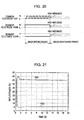
- Fig. 20 is a timing chart showing an image writing operation in a known electrophoresis display device.
- Fig. 20 potentials applied to a segment electrode 1035W of a segment performing a white display, a segment electrode 1035B of a segment performing a black display, and a common electrode 1037 are shown.
- Fig. 20 also shows an image writing period for displaying an image and an image maintaining period for maintaining the displayed image.
- the structure of an electrophoresis display device driven by a segment driving method is shown in Figs. 1, 2 , and 4 .
- the segment electrodes 1035W and 1035B in Fig. 20 correspond to two segment electrodes 35 of adjacent segments 40 shown in Fig. 2 and the common electrode 1037 corresponds to a common electrode 37.
- Fig. 21 shows measurement result of changes in reflectance of the known electrophoresis display device.
- a reference numeral 1001 denotes reflectance of a white display and a reference numeral 1002 denotes reflectance of a black display.
- the image writing period a high potential is applied to the segment electrode 1035B and a low potential is applied to the segment electrode 1035W.
- the common electrode 1037 is applied with a pulse in which high potentials and low potentials alternate.
- the image writing period begins from 0.5 seconds and continues for 0.5 seconds.
- the reflectance of a white display is increased and the reflectance of a black display is decreased.
- the image maintaining period begins.
- the segment electrode 1035B, 1035W, and the common electrode 1037 are in a high impedance state.
- the inventors have clarified that the lowering range of the contrast attributable to the kick back depends on moisture content of the electrophoresis display element by experiments.
- An advantage of some aspects of the invention is that it provides a driving method of an electrophoresis display device, an electrophoresis display device, and an electronic apparatus which are capable of maintaining a high contrast image after image writing.
- the driving method of an electrophoresis display device, the electrophoresis display device, and the electronic apparatus according to the invention have the following characteristics.
- an electrophoresis display device having a displaying portion which includes an electrophoresis element containing electrophoresis particles and disposed between a first electrode and a second electrode opposing one another and which consists of a plurality of pixels.
- the driving method includes a step of performing an image writing step in which an image is written into the displaying portion by applying a first potential or a second potential to the first electrodes separately provided for the pixels and applying a reference pulse in which the first potential and the second potential repeatedly alternate at a predetermined interval to the second electrode which is a common electrode shared by all the pixels, and a step of performing at least one contrast maintaining step including a short term interval step in which the second electrode and all the first electrodes fall in a high impedance state for five or less seconds and an auxiliary pulse inputting step in which at least one cycle of the reference pulse is applied to the second electrode and a potential which is equivalent to the potential applied during the image writing step is applied to the plurality of first electrodes while the reference pulse is applied.
- the contrast maintaining step be repeated several times.
- a period of the short term interval steps is changed each time the contrast maintaining step is performed.
- the contrast maintaining step continue until a next image writing step begins.
- the first electrode is applied with a potential which is equivalent to the potential applied during the image writing step, and the second electrode is in a high impedance state.
- a long term interval step in which the first electrodes and the second electrode stay in a high impedance state for 5 to 60 minutes, and a refresh step, in.which a pulse, which creates a potential difference between the first electrode and the second electrode, the potential difference being equivalent to that caused in the image writing step, is inputted to the second electrode, are performed.
- the short term interval step continue for 200 or more milliseconds.
- the width of the pulse used in the auxiliary pulse inputting step is set to be in a range from 1 to 20 milliseconds.
- the pulse width in the auxiliary pulse inputting step is preferably smaller than the pulse width in the image writing step.
- the change of the reflectance in the auxiliary pulse inputting step is relatively small in comparison with the change of reflectance in the image writing step. Since the input power is adjusted to comply with the decreased reflectance change, it is possible to avoid overwriting to the pixels and prevent contrast lowering attributable to the overwriting.
- a period of the auxiliary pulse inputting step is shortened each time the contrast maintaining step is performed.
- an electrophoresis device having a displaying portion which includes an electrophoresis element containing electrophoresis particles and disposed between a first electrode and a second electrode opposing to one another and which consists of a plurality of pixels, wherein a control portion performs at least one contrast maintaining operation including a short term interval operation in which the second electrode and all the first electrodes fall in a high impedance state for five or less seconds, and an auxiliary pulse inputting operation in which at least one cycle of a reference pulse is applied to the second electrode and a potential which is equivalent to the potential applied during an image writing step is applied to the plurality of first electrodes while the reference pulse is applied, after performing an image writing operation in which an image is written into the displaying portion by applying a first potential or a second potential to the first electrodes separately provided for the pixels and applying the reference pulse in which the first potential and the second potential repeatedly alternate at a predetermined interval to the second electrode which is a common electrode shared by all the pixels.
- control portion repeats the contrast maintaining operation a plurality of times.
- an electrophoresis display device capable of realizing a high contrast display.
- periods of the short term interval operations are different for every contrast maintaining operation.
- control portion continue the contrast maintaining operation until a next image writing operation begins.
- the short term interval operation is an operation for inputting a potential which is equivalent to the potential applied during the image writing operation to the first electrode and making the second electrode fall in a high impedance state.
- control portion performs a refresh operation including a long term interval operation for maintaining the first electrode and the second electrode to be in a high impedance state for 5 to 60 minutes and a refresh pulse inputting operation for inputting a pulse which causes a potential which is equivalent to the potential difference created during the image writing operation between the first electrode and the second electrode to the second electrode.
- the pixels and the control portion are connected to one another via pixel circuits provided for every pixel, respectively, and each of the pixel circuits includes a memory portion.
- control portion perform the short term interval operation for 200 or more milliseconds.
- control portion set a pulse width of the pulse to be in a range from 1 to 20 milliseconds in the auxiliary pulse inputting operation.
- a pulse width of a pulse used in the auxiliary pulse inputting operation be smaller than that of a pulse used in the image writing operation.
- the change of the reflectance in the auxiliary pulse inputting operation is smaller than that in the image writing operation. Accordingly, it is possible to avoid overwriting to the pixels by decreasing the input power to comply with the reflectance change, and thus is possible to prevent contrast lowering attributable to the overwriting.
- control portion shorten a period of the auxiliary pulse inputting operation each time the contrast maintaining operation is repeated.
- an electronic apparatus including the electrophoresis display device.
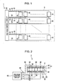
- Fig. 1 is a schematic plan view illustrating an electrophoresis display device 1.
- Fig. 2 is a view illustrating the sectional structure and electric configuration of the electrophoresis display device 1.
- Fig. 3 is a view illustrating a microcapsule 80.
- Figs. 4A, 4B, and 4C are explanatory views illustrating operation of white particles 82 and the black particles 83.
- Fig. 5 is a timing chart according to a first driving method.
- Figs. 6A and 6B are views illustrating reflectance change.
- Fig. 7 is a timing chart according to a second driving method.
- Fig. 8 is a timing chart according to a third driving method.
- Fig. 9 is a timing chart according to a fourth driving method.
- Fig. 10 is a timing chart according to a fifth driving method.
- Fig. 11 is a timing chart according to a sixth driving method.
- Fig. 12 is a schematic plan view illustrating an electrophoresis display device 100.
- Fig. 13 is a circuitry diagram illustrating a pixel 140.
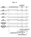
- Fig. 14 is a timing chart according to a seventh driving method.
- Fig. 15 is a circuitry diagram illustrating a pixel 240.
- Fig. 16 is a timing chart according to an eighth driving method.
- Fig. 17 is a front view illustrating a watch 300.
- Fig. 18 is a perspective view illustrating electronic paper 400.
- Fig. 19 is a perspective view illustrating an electronic notebook 500.
- Fig. 20 is a timing chart according to a known electrophoresis display device.
- Fig. 21 is a view illustrating reflectance change in the known electrophoresis display device.
- Fig. 1 shows the segment-driving-type electrophoresis display device 1.
- the electrophoresis display device 1 includes a displaying portion 5 in which a plurality of segments (pixels) 40 is arranged, and a voltage control circuit (control portion) 60.
- the voltage control circuit 60 and each of the segments 40 are electrically connected with one another via a segment electrode drive wiring 61 and a common electrode drive wiring 62.
- the segment driving type is a driving method in which a potential based on image data is directly inputted into each of the segments 40 from the voltage control circuit 60.
- Fig. 2 shows the sectional structure and electrical connection of the electrophoresis display device 1.
- the displaying portion 5 includes a substrate 30 consisting of a first substrate 34 and a plurality of segment electrodes (first electrodes) 35 disposed on the first substrate 34, an opposing substrate 31 consisting of a second substrate 36 and a common electrode (second electrode) 37 disposed on the second substrate 36, and electrophoresis elements 32, each consisting of a plurality of microcapsules 80, each containing electrophoresis particles (not shown) therein.
- the electrophoresis elements 32 are maintained between the segment electrode 35 and the common electrode 37 which face one another. Note that more than one electrophoresis element 32 may but need not be provided for each segment electrode 35. Similarly, more than one segment electrode 35 may be provided for an electrophoresis element 32.
- the segment electrode 35 is formed corresponding to segments 40, respectively and the common electrode 37 is a common electrode shared by all the segments 40.
- the electrophoresis display device 1 is configured to display an image at the common electrode 37 side.
- Each segment 35 is electrically connected to the voltage control circuit 60 via the segment electrode drive wiring 61 and a switch 65.
- the common electrode 37 is electrically connected to the voltage control circuit 60 via the common electrode drive wiring 62 and a switch 65.
- Fig. 3 shows a microcapsule 80.
- the microcapsule 80 has a grain diameter of about 50 micrometers.
- a material for the microcapsule 80 may be transparent polymer resin, such as acryl resin including polymethylmethacrylate and polyethylmethacrylate, urea resin, gelatine.
- a dispersion medium 81 Inside the microcapsule 80 are sealed a dispersion medium 81, a plurality of white particles (electrophoresis particles) 82, and a plurality of black particles (electrophoresis particles) 83.
- the dispersion medium 81 is a liquid which disperses the white particles 82 and the black particles 83 in the microcapsule 80.
- water an alcohol-based solvent, such as water, methanol, ethanol, isopropanol, butanol, octanol, and methyl cellosolve; a variety of esters, such as acetic ethyl and acetic butyl; ketone, such as acetone, methylethylketone, and methylisobutylketone; aliphatic hydrocarbon, such as pentane, hexane, and octane; cycloaliphatic hydrocarbon, such as cyclohexane and methylcyclohexane; aromatic hydrocarbon, such as benzene having a long-chain alkyl group, such as benzene, toluene, xylene, hexylbenzene, heptane,
- the white particles 82 are particles (polymer particles or inorganic particles) made of white pigment, such as titanium dioxide, zinc oxide, and antimony trioxide, and are negatively charged.
- the black particles 83 are particles (polymer particles or inorganic particles) made of black pigment, such as aniline black and carbon black, and are positively charged.
- a charge control agent containing an electrolyte, a surfactant, metal soap, a resin, gum, oil, varnish, and compound particles; a dispersant such as a titanium-coupling agent, an aluminum-coupling agent, and a silane-coupling agent; a lubricant; a stabilizing agent; and the like can be added to the pigment.
- Figs. 4A, 4B, and 4C show the operation of the white particles 82 and the black particles 83.
- segments 40B performing a black display and segments 40W performing a white display are depicted in order to compare movements of the white particles 82 and the black particles 83.
- a pixel electrode 35B of the segment 40B and a pixel electrode 35W of the segment 40W, which serve as the first electrodes, are applied with a potential corresponding to the image data.
- the pixel electrode 35W for performing a white display is applied with a low potential L which is a first potential.
- the pixel electrode 35B for performing a black display is applied with a high potential H which is a second potential.
- the common electrode 37 is applied with a reference pulse in which the low potential L serving as the first potential and the high potential H serving as the second potential alternates.
- Common swing driving means a driving method in which a pulse in which a high potential H and a low potential L are alternated with at least one cycle being applied to the common electrode 37 during an image writing period.
- the pixel electrode and the common electrode can be controlled by two values, the high potential H and the low potential L, it is possible to accomplish voltage lowering and simplify the circuit structure.
- a thin film transistor (TFT) is used as a switching element for each of the pixel electrodes 35 (35B and 35W), it is advantageous in that it is possible to ensure reliability of the TFT with low voltage driving.
- Fig. 4A shows the operation in which the low potential L in the first cycle is applied to the common electrode 37 in the common swing driving.
- the low potential L is applied to the common electrode 37 and the high potential H is applied to the segment electrode 35B. Accordingly, the black particles 83, which are charged positively, gather around the common electrode 37 and the white particles 82, which are negatively charged, gather around the segment electrode 35B.
- both of the common electrode 37 and the segment electrode 35W are applied with the same low potential L. Accordingly, there is no potential difference between the common electrode 37 and the segment electrode 35W, and thus the particles do not move.
- Fig. 4B shows the operation in which the high potential H is applied to the common electrode 37 in the first cycle of pulse.
- the common electrode 37 is applied with the high potential H and the segment electrode 35W is applied with the low potential L. Accordingly, the positively charged black particles 83 move toward the segment electrode 35W and the negatively charged white particles 82 move toward the common electrode 37.
- both of the common electrode 37 and the segment electrode 35B are applied with the high potential H. Accordingly, there is no potential difference between the common electrode 37 and the segment electrode 35B, and thus the particles do not move and this state is maintained.
- Fig. 4C shows the operation after the first cycle of pulse is applied by the common swing driving method.
- the white particles 82 gather around the segment electrode 35B and the black particles 83 gather around the common electrode 37. Accordingly, a black display is shown from the common electrode 37 side, which serves as a displaying surface.
- the black particles 83 gather around the segment electrode 35W and the white particles 82 gather around the common electrode 37 side. Accordingly, a white display is shown from the common electrode 37 side which serves as a displaying surface.
- Fig. 5 shows a timing chart according to a first driving method.
- the electrophoresis display device uses a driving method by which high contrast can be realized by increasing reflectance of a white display and decreasing reflectance of a black display after the image writing operation.
- the driving method according to a first embodiment performs a contrast maintaining step a plurality of times after the image writing step.
- the image writing step is the same as an image writing period of Fig. 20 . That is, the image writing step is another expression of the image writing period.
- the driving method of the embodiment includes an image writing step and a contrast maintaining step.
- the timing chart shown in Fig. 5 is for the segments 40B (black display) and the segments 40W (white display) shown in Figs. 4A, 4B, and 4C .
- Fig. 5 shows potentials applied to the common electrode 37, the segment electrode 35B of the segment 40B, and the segment electrode 35W of the segment 40W.
- a voltage is supplied for each of the segments 40 on the basis of the display image and a desired image is displayed on the displaying portion 30.
- the common electrode 37 is applied with the reference pulse in which the low potential L and the high potential H periodically alternates.
- the reference pulse supplied to the common electrode 37 is a pulse with a cycle of 40 milliseconds consisting of a period for the low potential L (0V) of 20 milliseconds and a period for the high potential H (15V) of 20 milliseconds.
- the segment electrode 35B of the segment 40B performing a black display is applied with the high potential H and the segment electrode 35W of the segment 40W performing a white display is applied with the low potential L.
- the segment 40B performs a black display and the segment 40W performs a white display.
- a contrast maintaining step begins.
- a short term interval step and an auxiliary pulse inputting step is performed.
- the short term interval step will be described.
- the segment electrodes 35B and 35W and the common electrode 37 are electrically disconnected from one another and stay in a high impedance state.
- a period of the short interval step is in a range from 200 milliseconds to 5 seconds.
- the period for the short term interval step is shorter than 200 milliseconds, the auxiliary pulse inputting step is performed in the state in which the reflectance nearly does not change after the image writing. Accordingly, it is difficult to obtain advantageous effects. As a result, overwriting occurs and thus the contrast is likely to be lowered again.
- the period for the short term interval step exceeds 5 seconds
- the decreased amount of the reflectance of the white display is increased
- the increased amount of the reflectance of the black display is increased, resulting in a significant drop in the contrast. If the auxiliary pulse inputting step is performed in this state, the change of the reflectance in the auxiliary pulse inputting step is visibly recognized by a user, and a display flashes. That is, a user is visibly stressed.
- auxiliary pulse inputting step a single cycle of an auxiliary pulse having a period of the low potential L and a period of the high potential period H is inputted to the common electrode 37.
- This auxiliary pulse is a pulse having a low potential of 0V, a high potential of 15V, and a pulse width of 20 milliseconds (a cycle of 40 milliseconds) like the reference pulse in the image writing step.
- the segment electrode 35B is applied with the high potential H (15V) and the segment electrode 35W is applied with the low potential L (0V).
- the contrast maintaining step consisting of the short term interval step and the auxiliary pulse inputting step is repeatedly performed a plurality of times. Accordingly, the driving method can compensate the contrast lowering occurring after the first time of contrast maintaining step. That is, since the contrast lowering attributable to the kick back continues for a predetermined period after the image writing step, and the reflectance continuously changes during the period, the reflectance continues to change even after the contrast maintaining step. Accordingly, during a period in which the state of the electrophoresis element 32 is stabilized and the reflectance change is recovered, the contrast maintaining step is repeatedly performed. Therefore, a desired contrast level can be maintained.
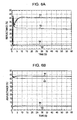
- Figs. 6A and 6B reflectance changes in the driving method according to the invention and the known method are compared.
- Fig. 6A shows the result of change in reflectance with time under dry condition
- Fig. 6B shows the result of change in reflectance with time under normal condition.
- the dry condition means the state in which the electrophoresis element contains 0% Rh of humidity.
- the graph shown in Fig. 6A is data obtained using an electrophoresis element stored for a week under condition of 60°C and 0% Rh.
- Normal condition means the state of temperature of 25 ⁇ 2.5°C and relative humidity of 65 ⁇ 20% Rh.
- the graph shown in Fig. 6B is data obtained using an electrophoresis element stored for a week under the normal condition.
- the data of the graphs 6A and 6B is measured under the condition of temperature 25°C and relative humidity 65% Rh.
- the contrast maintaining step is repeatedly performed 10 times after the image writing step.
- the short term interval step is 800 milliseconds and the auxiliary pulse inputting step is 40 milliseconds (pulse width of 20 milliseconds in a single cycle).
- the known driving method provided for the purpose of comparison is the same as the driving method of the invention except that the contrast maintaining step is not performed.
- reference numeral 91 denotes reflectance of a white display according to the driving method of the invention
- reference numeral 92 denotes reflectance of a black display according to the driving method of the invention
- reference numeral 93 denotes reflectance of a white display according to the known driving method
- reference numeral 94 denotes reflectance of a black display according to the known driving method.
- Figs. 6A and 6B As shown in Figs. 6A and 6B , according to the known driving method, reflectance of a white display is decreased after the image writing and the reflectance of a black display is increased after the image writing. In particular, under the dry condition of Fig. 6A , the reflectance decrease of a white display is remarkable, and the reflectance is decreased by 20% or more for 5 seconds after the image writing thanks to the kick back phenomenon. Under the normal condition, the reflectance of a white display is decreased by 5% or more by the kick back phenomenon.
- the contrast after 50 minutes passes in Fig. 6A is about 4.0 and 8.7 when employing the known driving method and the present invention driving method, respectively. That is, it is clarified that the contrast remarkably improves.
- the values are ratios of the reflectance of a white display to the reflectance of a black display.
- the auxiliary pulse inputting step since the auxiliary pulse inputting step is performed, the reflectance decrease of a white display after the image writing is suppressed, and the reflectance increase of a black display after the image writing is suppressed. Accordingly, it is possible to avoid deterioration in contrast after image writing and to realize a high contrast display.
- the contrast maintaining step it is possible to completely compensate the contrast decrease attributable to the kick back by performing the contrast maintaining step a plurality of times to comply with the period in which the reflectance varies due to the kick back after the image writing, and to obtain desired reflectance for both the white display and black display. Further, since the contrast is increased at the transition time between the contrast maintaining step and an image maintaining period in comparison with the known driving method, deterioration of the display quality occurring after a maintaining period terminates is decreased and it is possible to obtain a comprehensively high quality display.
- the contrast maintaining step is performed 10 times
- the number of times is not limited thereto. That is, the number of times is set to be in a range from 1 to several tens.
- a single cycle of the reference pulse used in the image writing step is supplied to the common electrode 37 as the auxiliary pulse, but the cycle of the auxiliary pulse applied to the common electrode 37 need not be limited thereto.
- the pulse may be a half cycle or less or more than one cycle.
- the auxiliary pulse can be applied during only a period of the high potential H or a period of the low potential L.
- the auxiliary pulse is inputted during only a period of the high potential H, it is possible to suppress the decrease of the reflectance of a white display.
- the auxiliary pulse is inputted during only a period of the low potential L, it is possible to suppress the decreased of the reflectance of a black display.
- the effect of compensating the reflectance change becomes larger and thus the number of repetitions may be set according to the characteristic of the electrophoresis element 32.
- the pulse width of the auxiliary pulse is set to 20 milliseconds but may be set in a range from 1 to 40 milliseconds. That is, the pulse width may be set to be as short as possible in the range in which the contrast recovery effect can be obtained by the auxiliary pulse input but to be as long as possible in the range in which the overwriting does not occur.
- the auxiliary pulse is set to have the same cycle time (40 milliseconds) as the reference pulse and that the time the second potential (H potential) is applied be the same as or shorter than the pulse width of the reference pulse. It is preferable that the pulse width of the auxiliary pulse is in the range from 5 to 20 milliseconds. With such a range, it is possible to surely obtain the recovery effect of the contrast by the input of the auxiliary pulse and it is not likely to observe the overwriting.
- the pulse width of the low potential and the pulse width of the high potential are set to be the same (20 milliseconds) in the auxiliary pulse inputting step, but these may be differently set.
- a period of the low potential L is set to 20 milliseconds and a period of the high potential H is set to 30 milliseconds.
- a period of a white display is 1.5 times a period of a black display.
- a period of the short term interval step is set to be 200 or more seconds.
- the interval is less than 200 milliseconds, since a voltage is applied to the electrodes in the state in which the reflectance does not nearly change from the reflectance of the image writing time, the same phenomenon as the overwriting occurs and the amount of the reflectance change is likely to be increased.
- the overwriting to the segments 40B and 40W does not occur and it is possible to suppress the reflectance decrease of a white display after the image writing, suppress the reflectance increase of a black display after the image writing, and realize a high contrast display.
- a period of the short term interval step is shorter than 5 seconds.
- the reflectance changes by a significant amount due to the kick back. Further, the reflectance change after the contrast maintaining step is visibly recognized by a user, and it is likely to impart unpleasantness to the user.
- a period of the short term interval step is in the range from 500 milliseconds to 2 seconds.
- a driving method of the segment-driving-type electrophoresis display device 1 shown in Figs. 1 and 2 will be described.
- a contrast maintaining step is performed only once.
- Fig. 7 shows a timing chart illustrating the driving method according to the second embodiment.
- the driving method according to the embodiment has an image writing step and a contrast maintaining step. After the contrast maintaining step is performed only one time, every electrode falls into a high impedance state.
- the operations of the image writing and the contrast maintaining step are the same as the first embodiment.
- an auxiliary pulse inputting step is performed only one time, it is possible to decrease the load applied to white particles 82 and black particles 83, it is possible to prevent overwriting to a segment 40B and a segment 40W, and it is possible to save power.
- the driving method according to the second embodiment is possibly less advantageous than the driving method according to the first embodiment, it is also possible to improve contrast since the reflectance of a white display increases and the reflectance of a black display decreases.
- the driving method according to the third embodiment is a driving method in which a pulse cycle in an image writing step is shorter than a pulse cycle in an auxiliary pulse inputting step.
- Fig. 8 shows a timing chart of the driving method according to the third embodiment.
- the driving method of this embodiment includes an image writing step and a contrast maintaining step. Details of the operation of the image writing step are the same as the first embodiment. During the contrast maintaining step, details of the operation of the short term interval are the same as the driving method according to the first embodiment.
- a pulse width of an auxiliary pulse inputted to the common electrode 37 in the auxiliary pulse inputting step is set to be shorter than a pulse width of a reference pulse applied to the common electrode 37 in the image writing step.
- the auxiliary pulse is continuously inputted to the common electrode 37.
- the pulse width of the auxiliary pulse can be decreased to 5 milliseconds when the pulse width is 20 milliseconds in the image writing step.
- the pulse width means a period of a second potential (high potential H) in a single cycle of a common swing driving method and the cycle time (frequency) of the auxiliary pulse is the same as that of the reference pulse.
- the pulse width of the auxiliary pulse can be changed in the range from 1 to 20 milliseconds according to the pulse width in the image writing step.
- a plurality of cycles of the auxiliary pulse is continuously inputted in the auxiliary pulse inputting step.
- the number of times of repetition is not particularly limited but can be changed in a range by which the overwriting does not occur.
- the auxiliary pulse inputting step is continued between the current short term interval step and a next image writing step (image update of a next frame).
- the auxiliary pulse may be shorter than 1 cycle. In such a case, only either a high potential H period or a low potential L period may be set.
- the short term interval step may be set for every cycle of the auxiliary pulse inputting step like the first embodiment.
- the cycle of the auxiliary pulse it is not limited to be the same as the reference pulse, but may be different from that of the reference pulse as long as the pulse width of the auxiliary pulse is the above-described period. By this method, it is possible to obtain the above-described advantages.
- the auxiliary pulse inputting step since the auxiliary pulse having a pulse width shorter than that of the pulse of the image writing step is applied to the common electrode 37, it is possible to perform an operation for recovering the reflectance by driving the electrophoresis element 32 with short steps. Accordingly, it is possible to decrease the load applied to the white particles 82 and the black particles 83, and it becomes easy to suppress the overwriting in the auxiliary pulse inputting step. Further, by continuing the auxiliary pulse inputting step until a next image writing step begins, it is possible to obtain a high contrast display.
- the driving method according to the fourth embodiment is a driving method in which a refresh step is performed after the auxiliary pulse inputting period.
- Fig. 9 shows a timing chart of the driving method according to the fourth embodiment.
- the driving method includes an image writing step, a contrast maintaining step, and a refresh step. Details of the operations of the image writing step and the contrast step of these steps are the same as in the second embodiment, in the first embodiment, or in the third embodiment.
- the refresh step includes a long term interval step and a refresh pulse inputting step, and is to suppress the contrast lowering during a relatively long period after the contrast maintaining step.
- the segment electrode 35B, the segment electrode 35W, and the common electrode 37 are electrically isolated from one another and fall into a high impedance state.
- the segment electrode 35B is applied with the high potential H and the segment electrode 35W is applied with the low potential L.
- the common electrode 37 is applied with a refresh pulse in which a high potential H period and a low potential L period alternate. That is, the potentials of the segment electrode 35W and 35B and the common electrode 37 in the image writing step are applied to the corresponding electrodes.
- the refresh pulse applied to the common electrode 37 has the length of at least one cycle or longer. In the case in which the refresh pulse is shorter than one cycle, only a high potential H period or a low potential L period is set as the refresh pulse. However, in this case, it is possible to compensate the variation of the reflectance of at least one of the white display and the black display.
- the refresh step is provided in the image maintaining period after the auxiliary pulse inputting step, it is possible to effectively prevent the contrast lowering even after the contrast maintaining step. Therefore, it is possible to maintain the contrast for a relatively long period.
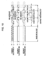
- the driving method according to the fifth embodiment is a driving method in which a period of a short term interval step is decreased by repeating a contrast maintaining step a plurality of times.
- Fig. 10 shows a timing chart of the driving method according to the fifth embodiment.
- the driving method according to this embodiment includes an image writing step and a plurality of contrast maintaining steps.
- the operation of the image writing step is the same as the driving method according to the first embodiment.
- the contrast maintaining step is performed a plurality of times, but a period of the short term interval step is changed each time the contrast maintaining step is performed.
- the period of the first short term interval step is 800 milliseconds
- the period of the second short term interval step is 500 milliseconds
- the period of the third short term interval step is 300 milliseconds.
- the period of each short term interval step is not limited in detail, but may be changed according to the display characteristic of the electrophoresis display device.
- the period of the short term interval step is set to be 200 milliseconds or longer.
- the operations (pulse width, period, and number of times of repetition) of the auxiliary pulse inputting step may be different according to the kinds of the previous embodiment.
- the operations of the auxiliary pulse inputting steps in the plurality of times of the contrast maintaining step are the same.
- the reflectance of a white display is increased to be closer to the reflectance at the time of the image writing and the fluctuation of the reflectance becomes decreased. Further, the reflectance of a black display changes in the same manner as the reflectance of a white display.
- a driving method of the segment-driving-type electrophoresis display device 1 shown in Figs. 1 and 2 will be described.
- the common electrode 37 is electrically disconnected in the short term interval step of the contrast maintaining step and the segment electrodes 35B and 35W are applied with the potential applied in the image writing step.
- Fig. 11 shows a timing chart according to the sixth embodiment.
- the driving method of the sixth embodiment includes an image writing step and a plurality of contrast maintaining steps. Since the image writing step is the same as in the first driving method, description thereof will be omitted.
- the contrast maintaining step includes a short term interval step and an auxiliary pulse inputting step.
- the short term interval step the common electrode 37 is electrically disconnected, and the segment electrodes 35W and 35B are applied with potentials which are equivalent to the potentials applied in the image writing step. That is, the segment electrode 35B is applied with the high potential H and the segment electrode 35W is applied with the low potential L.
- auxiliary pulse inputting step according to the sixth embodiment is the same as in any of the driving methods according to first to fifth embodiments, description thereof will be omitted.
- the above embodiments are described with an example of the segment-driving type electrophoresis display device but may not be limited thereto.
- the embodiments can be applied to an active matrix-driving type electrophoresis display device shown in Fig. 12 . Even in such a case, the same advantages as the above-described embodiments can be obtained.
- a driving method according to a seventh embodiment of the invention will be described with reference to an active matrix-driving type electrophoresis display device.
- Fig. 12 shows an active matrix-driving type electrophoresis driving method 100.
- the electrophoresis display device 100 includes a displaying portion 105 in which a plurality of pixels 140 is arranged in a matrix form, a scan line driving circuit 161 and a data line driving circuit 162 arranged to surround the displaying portion 105, and a controller 163.
- a plurality of scan lines 161 a extend from the scan line driving circuit 161 toward the displaying portion 105 and a plurality of data lines 162a extend from the data line driving circuit 162 toward the displaying portion 105.
- the scan line driving circuit 161 and the data line driving circuit 162 are connected to the controller 163, which is a control portion of the electrophoresis display device 100.
- the scan line driving circuit 161 and the pixels 140 are connected to one another via the plurality of scan lines 161a (Y1, Y2, ..., and Ym) extending in an extending direction of the data line driving circuit 162.
- the data line driving circuit 162 and the pixels 140 are connected to one another via a plurality of data lines 162a (X1, X2, ..., and Xn) extending in an extending direction of the scan line driving circuit 161.
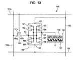
- Fig. 13 is a circuitry diagram showing the pixel 140.
- the pixel 140 includes a switching element (pixel circuit) 141, a latch circuit (memory circuit) 190 consisting of eight transistors, and an electrophoresis element 132.
- the electrophoresis element 132 is interposed between the pixel electrode 135 and the common electrode 137.
- the common electrode 137 is a common electrode shared by all the pixels 140.
- the common electrode 137 side is a displaying surface.
- the switching element 141 is a field effect type n-channel transistor.
- a gate 141 a of the switching element 141 is connected to the scan line 161 a, an input terminal 141b of the switching element is connected to the data line 162a, and an output terminal 141 c of the switching element is connected to the latch circuit 190.
- the latch circuit 190 includes an inverter circuit consisting of p-channel transistors 191 and 192 (the gates of which are) connected in parallel with one another and n-channel transistors 195 and 196 connected in parallel with one another and an inverter circuit consisting of p-channel transistors 193 and 194 connected in parallel with one another and n-channel transistors 197 and 198 connected in parallel with one another.
- the latch circuit 190 has an input terminal N1 and an output terminal N2. At the input terminal N1, the p-channel transistor 192 and the n-channel transistor 195 are connected to one another, and at the output terminal N2, the p-channel transistor 194 and the n-channel transistor 197 are connected to one another.
- Gates of the p-channel transistors 191 and 192 and the n-channel transistors 195 and 196 are connected to the output terminal N2 and the pixel electrode 135, and gates of the p-channel transistors 193 and 194 and the n-channel transistors 197 and 198 are connected to the input terminal N1 and the switching element 141.
- the p-channel transistors 191 and 193 are connected to the high potential power source line 150, and the n-channel transistors 196 and 198 are connected to the low potential power source line 149.
- the latch circuit 190 having such a structure is a static random access memory (SRAM).
- SRAM static random access memory
- arranging two transistors such as the p-channel transistors 191 and 192 to be in parallel with one another serves to decrease the leak current.
- double gate i.e. arranging two transistors
- a single gate structure i.e. arranging transistors one by one
- the single gate structure can be also applied to the structure of the latch circuit and the transmission gate of Fig. 15 .
- a driving method according to a seventh embodiment is a driving method associated with the active matrix driving type electrophoresis display device 100.
- the driving method according to the seventh embodiment is a driving method which maintains image data by driving a latch circuit 190 at the minimum level by lowering a potential of a high potential power source line 150 in the short interval step of the contrast maintaining step.
- Fig. 14 is a timing chart illustrating the driving method according to the seventh embodiment. As shown in Fig. 14 , the driving method according to this embodiment includes an image writing step and a contrast maintaining step.
- a pixel 140 will be described with reference to a pixel 140 performing a black display and a pixel 140 performing a white display, separately.
- a common electrode 137 a low potential power source line 149, a high potential power source line 150, a pixel electrode 135B of the pixel 140 performing a black display, an input terminal N1 B, a pixel electrode 135W of the pixel 140 performing a white display, and an input terminal N1W are shown.
- the pixel electrode 135B is applied with the high potential H.
- the pixel electrode 135W is applied with the low potential L.
- the common electrode 137 is applied with the same potential as the potential applied to the common electrode 35 in the first embodiment and the image is written.
- the contrast maintaining step includes a short term interval step and an auxiliary pulse inputting step.
- the short term interval step the common electrode 137 is electrically disconnected, and comes to fall into a high impedance state.
- the potential of the high potential power source line 150 can be lowered to the minimum potential H1 which can drive the latch circuit 190, and to 1V, for example.
- the minimum potential H1 which can.drive the latch circuit 190 means a potential which can maintain the memory of the latch circuit.
- the minimum potential H1 is set to 1V, but may be set to be a different voltage, taking the characteristic of the latch circuit into consideration.
- the potential H1 is applied to the pixel electrode 135B and the low potential L is applied to the pixel electrode 135W.
- the potential of the high potential power source line 150 recovers to the high potential H, and the pixel electrode 135B is applied with the high potential H.
- the common electrode 137 is applied with the auxiliary pulse which is the same as in any one of the first to the sixth driving methods.
- the period of the contrast maintaining step and the number of times of repetition can be set in the same manner as in the above-described embodiments.
- the short term interval step and the auxiliary pulse inputting step are also set in the same manner as in the above-described embodiments.
- the latch circuit 190 is driven at a low potential in the short term interval step and the image data inputted into the latch circuit 190 in the image writing step can be maintained. Accordingly, in the auxiliary pulse inputting step, it is satisfactory that the image data is not inputted again to the pixel electrodes 135B and 135W. Therefore, it is possible to suppress the load of the controller 163. Further, since the potential of the high potential power source line 150 is lowered, it is possible to suppress the power consumption to a low level.
- Fig. 15 is a circuitry diagram showing the pixel 240 having a switching circuit 170.
- the switching circuit 170 is disposed between a latch circuit 190 and a pixel electrode 135.
- the latch circuit 190 is the same as in the seventh embodiment.
- the switching circuit 170 includes two transmission gates 171 and 176.
- the transmission gate 171 consists of n-channel transistors 172 and 174 connected in parallel with one another and p-channel transistors 173 and 175 connected in parallel with one another.
- An input terminal of the transmission gate 171 is connected to a second control line 182.
- the transmission gate 176 consists of n-channel transistors 177 and 179 connected in parallel with one another and p-channel transistors 178 and 180 connected in parallel with one another. An input terminal of the transmission gate 176 is connected to a first control line 181.
- Gates of the n-channel transistors 172 and 174 and the p-channel transistors 178 and 180 are connected to an input terminal N1 of the latch circuit 190.
- gates of the p-channel transistors 173 and 175 and the n-channel transistors 177 and 179 are connected to an output terminal N2 of the latch circuit 190.
- Output terminals of the transmission gates 171 and 176 are connected to the pixel electrode 135.
- the switching circuit 170 is structured in a manner such that the transmission gate 171 or the transmission gate 176 is driven on the basis of the image data inputted into the latch circuit 190. With such a structure, when the transmission gate 171 is driven, the potential of the second control line 182 is inputted into the pixel electrode 135, and when the transmission gate 176 is driven, the potential of the first control line 181 is inputted into the pixel electrode 135.
- a driving method according to an eighth embodiment of the invention is a driving method according to a pixel 240 including a switch circuit 170.
- the eighth driving method is a driving method of electrically disconnecting a first control line 181 from a second control line 182 by lowering a potential of a latch circuit 190 to the minimum level in a short term interval step of a contrast maintaining step.
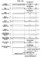
- Fig. 16 is a timing chart showing the driving method according to the eighth embodiment of the invention.
- a pixel 240B performing a black display and a pixel 240W performing a white display will be separately described.
- the driving method has an image writing step and a contrast maintaining step.
- the image writing step if the low potential L is applied to the input terminal N1B as image data, the output terminal N2B becomes a high potential H, and a transmission gate 176 is driven. When the transmission gate 176 is open, the potential of the first control line 181 is applied to the pixel electrode 135B.
- the pixel electrode 135B is applied with the high potential H.
- the output terminal N2W becomes the low potential L and the transmission gate 171 is driven.
- the transmission gate 171 turns on, the potential of the second control line 182 is applied to the pixel electrode 135W.
- the pixel electrode 135W is applied with the low potential L.
- the common electrode 137 is applied with a pulse which is the same as the reference pulse applied to the common electrode 35.
- the short term interval step and the auxiliary pulse inputting step are performed.
- the common electrode 137 is electrically disconnected and falls into a high impedance state.
- the potential of the high potential power source line 150 is lowered to the minimum level H1 as low as possible to a level at which the latch circuit 190 can be driven like the seventh driving method and thus the operation of the latch circuit 190 is continued.
- the first control line 181 and the second control line 182 are electrically disconnected from one another, and fall into a high impedance state.
- the image data is held in the latch circuit 190, and the transmission gate 171 or the transmission gate 176 is driven.
- the first control line 181 and the second control line 182 are electrically disconnected from one another the pixel electrodes 135B and 135W fall into a high impedance state.
- the potential of the high potential power source line 150 recovers to the high potential H. Further, potentials of the first control line 181 and the second control line 182 recover to the potential in the image writing step. In greater detail, the first control line 181 is applied with the high potential H and the second control line 182 is applied with the low potential L.
- the common electrode line 137 is applied with the auxiliary pulse which is the same as in any one of the first to sixth embodiments.
- the period of the contrast maintaining step and the number of times of repetition can be set in the same manner as any of the embodiments.
- the short term' interval step and the auxiliary pulse inputting step are also set in the same manner as any of the embodiments.
- the latch circuit 190 can be driven at the optimum potential, it is possible to maintain the image data, suppressing the power consumption in the short term interval step.
- Fig. 17 shows a wrist watch 300.
- the wristwatch 300 consists of a clock casing 302, and a pair of bands 303 connected to the watch casing 302.
- the electrophoresis display device (display panel) 305 On the front face of the watch casing 302, the electrophoresis display device (display panel) 305, a second hand 321, a minute hand 322, and an hour hand 323 are disposed.
- a winding crown 310 and a manipulation button 311 are disposed as manipulators.
- the winding crown 310 is connected to a winding stem (not shown) disposed in the casing, and is integrally formed with the winding stem.
- the winding crown can be freely pushed or pulled in multiple stages (for example, 2 states), and is freely rotatable.
- a background image, character strings such as date and time, or hands of a clock, such as an hour hand, a minute hand, and a second hand can be displayed.
- the physical hands 321-323 can be dispensed with if desired.
- the electrophoresis display device With the use of the electrophoresis display device according to the invention, it is possible to realize a watch 300 equipped with a displaying portion which is capable of suppressing a decrease in the reflectance of a white display right after image writing and suppressing an increase in the reflectance of a black display right after image writing, and which thus has high contrast.
- Fig. 18 shows the structure of the electronic paper 400.
- the electronic paper 400 employs the electrophoresis display device according to the invention as a displaying portion 401.
- the electronic paper 400 is constituted as a main body 402 formed of a rewritable sheet having flexibility and paper-like texture and softness.
- Fig. 19 shows the structure of an electronic notebook 500.
- the electronic notebook 500 has a structure in which a plurality of pieces of the electronic paper 400 shown in Fig. 18 is filed between covers 501.
- the cover 501 is equipped with a display data input unit (not shown) for allowing display data sent from external devices to be inputted. With this structure, it is possible to change and update the display contents in the state in which the plurality of pieces of electronic paper 400 is filed, according to the display data.
- the electrophoresis display device By applying the electrophoresis display device according to the invention to electronic paper 400 or an electronic notebook 500, it is possible to suppress a decrease in the reflectance of the white display right after the image writing, suppress an increase in the reflectance of the black display right after the image writing, and thus to realize the electronic paper 400 or the electronic notebook 500 having a displaying portion having high contrast.
- the electrophoresis display device can be employed as a displaying portion of any other suitable electronic apparatus, such as a cellular phone and a portable video player.
Landscapes
- Engineering & Computer Science (AREA)
- Physics & Mathematics (AREA)
- Computer Hardware Design (AREA)
- General Physics & Mathematics (AREA)
- Theoretical Computer Science (AREA)
- Electrochromic Elements, Electrophoresis, Or Variable Reflection Or Absorption Elements (AREA)
- Control Of Indicators Other Than Cathode Ray Tubes (AREA)
Applications Claiming Priority (1)
| Application Number | Priority Date | Filing Date | Title |
|---|---|---|---|
| JP2007237637A JP5071014B2 (ja) | 2007-09-13 | 2007-09-13 | 電気泳動表示装置の駆動方法、電気泳動表示装置、及び電子機器 |
Publications (2)
| Publication Number | Publication Date |
|---|---|
| EP2037443A2 true EP2037443A2 (fr) | 2009-03-18 |
| EP2037443A3 EP2037443A3 (fr) | 2009-11-25 |
Family
ID=40120296
Family Applications (1)
| Application Number | Title | Priority Date | Filing Date |
|---|---|---|---|
| EP08253004A Ceased EP2037443A3 (fr) | 2007-09-13 | 2008-09-11 | Procédé de commande de dispositif d'affichage électrophorétique, dispositif d'électrophorèse et appareil électronique |
Country Status (6)
| Country | Link |
|---|---|
| US (1) | US8294663B2 (fr) |
| EP (1) | EP2037443A3 (fr) |
| JP (1) | JP5071014B2 (fr) |
| KR (1) | KR101587649B1 (fr) |
| CN (1) | CN101388180B (fr) |
| TW (1) | TWI450240B (fr) |
Families Citing this family (17)
| Publication number | Priority date | Publication date | Assignee | Title |
|---|---|---|---|---|
| JP5320757B2 (ja) * | 2008-02-01 | 2013-10-23 | セイコーエプソン株式会社 | 電気泳動表示装置の駆動方法、電気泳動表示装置及び電子機器 |
| JP5444953B2 (ja) * | 2009-02-06 | 2014-03-19 | セイコーエプソン株式会社 | 電気泳動表示装置の駆動方法、電気泳動表示装置、及び電子機器 |
| US8481873B2 (en) * | 2009-09-30 | 2013-07-09 | Freescale Semiconductor, Inc. | Capacitive touch sensor device configuration systems and methods |
| JP5338622B2 (ja) * | 2009-11-04 | 2013-11-13 | セイコーエプソン株式会社 | 電気泳動表示装置の駆動方法、電気泳動表示装置、及び電子機器 |
| JP5601470B2 (ja) * | 2010-12-01 | 2014-10-08 | セイコーエプソン株式会社 | 電気泳動表示装置の駆動方法、電気泳動表示装置、及び電子機器 |
| JP5601469B2 (ja) | 2010-12-01 | 2014-10-08 | セイコーエプソン株式会社 | 電気泳動表示装置の駆動方法、電気泳動表示装置、及び電子機器 |
| JP2012137575A (ja) * | 2010-12-27 | 2012-07-19 | Hitachi Chem Co Ltd | 懸濁粒子装置,懸濁粒子装置を用いた調光装置及びそれらの駆動方法 |
| JP6014973B2 (ja) * | 2011-07-05 | 2016-10-26 | 大日本印刷株式会社 | 画像表示装置及びその駆動方法 |
| JP5845852B2 (ja) * | 2011-11-29 | 2016-01-20 | 富士ゼロックス株式会社 | 画像表示媒体駆動装置、画像表示装置、及び画像表示媒体駆動プログラム |
| TWI526765B (zh) | 2013-06-20 | 2016-03-21 | 達意科技股份有限公司 | 電泳顯示器及操作電泳顯示器的方法 |
| JP2015169902A (ja) * | 2014-03-10 | 2015-09-28 | 大日本印刷株式会社 | 反射型表示装置の駆動方法 |
| JP6710936B2 (ja) * | 2015-11-05 | 2020-06-17 | 凸版印刷株式会社 | 電気泳動表示装置及びその駆動方法 |
| US9985126B2 (en) | 2016-03-04 | 2018-05-29 | Infineon Technologies Ag | Semiconductor device comprising a first gate electrode and a second gate electrode |
| US10128750B2 (en) * | 2016-03-04 | 2018-11-13 | Infineon Technologies Ag | Switched-mode power converter with an inductive storage element and a cascode circuit |
| CN107331354B (zh) * | 2017-08-10 | 2019-09-03 | 上海中航光电子有限公司 | 电泳显示面板及其驱动方法和显示装置 |
| JP7148324B2 (ja) * | 2017-12-11 | 2022-10-05 | Tianma Japan株式会社 | 光線方向制御装置及び光線方向制御素子の駆動方法 |
| CN114582293B (zh) * | 2022-03-10 | 2023-08-04 | 广东奥素液芯微纳科技有限公司 | 一种微流控有源矩阵驱动电路及微流控装置 |
Citations (2)
| Publication number | Priority date | Publication date | Assignee | Title |
|---|---|---|---|---|
| JPH03213827A (ja) | 1990-01-18 | 1991-09-19 | Nippon Mektron Ltd | 電気泳動表示パネルの駆動装置 |
| JP2002116733A (ja) | 2000-06-22 | 2002-04-19 | Seiko Epson Corp | 電気泳動表示装置の駆動方法、駆動回路、および電子機器 |
Family Cites Families (20)
| Publication number | Priority date | Publication date | Assignee | Title |
|---|---|---|---|---|
| JP4785300B2 (ja) * | 2001-09-07 | 2011-10-05 | 株式会社半導体エネルギー研究所 | 電気泳動型表示装置、表示装置、及び電子機器 |
| KR20040089702A (ko) * | 2002-03-05 | 2004-10-21 | 코닌클리케 필립스 일렉트로닉스 엔.브이. | 전기영동 디스플레이 디바이스 및 밝기 레벨을 복구하기위한 구동 수단 |
| TWI240842B (en) * | 2002-04-24 | 2005-10-01 | Sipix Imaging Inc | Matrix driven electrophoretic display with multilayer back plane |
| JP4325164B2 (ja) * | 2002-09-11 | 2009-09-02 | セイコーエプソン株式会社 | 電気光学装置、電気光学装置の駆動方法及び電子機器 |
| JP3873149B2 (ja) | 2002-12-11 | 2007-01-24 | 株式会社日立製作所 | 表示装置 |
| TW200511178A (en) * | 2003-08-25 | 2005-03-16 | Koninkl Philips Electronics Nv | Method of compensating image instability and improving greyscale accuracy for electrophoretic displays |
| JP2007505350A (ja) * | 2003-09-11 | 2007-03-08 | コニンクリユケ フィリップス エレクトロニクス エヌ.ブイ. | リセットパルス及びハードウェア駆動を用いる画像品質の改善を伴う電気泳動ディスプレイ |
| JP4213637B2 (ja) * | 2003-09-25 | 2009-01-21 | 株式会社日立製作所 | 表示装置及びその駆動方法 |
| JP2007507735A (ja) * | 2003-09-30 | 2007-03-29 | コーニンクレッカ フィリップス エレクトロニクス エヌ ヴィ | 中間光学状態を有する電気泳動ディスプレイでのフリッカを低減するリセットパルス駆動 |
| JP2007511794A (ja) * | 2003-11-17 | 2007-05-10 | コーニンクレッカ フィリップス エレクトロニクス エヌ ヴィ | Dc平衡型オーバー・リセット駆動を有する双安定ディスプレイ |
| EP1687801A1 (fr) * | 2003-11-21 | 2006-08-09 | Koninklijke Philips Electronics N.V. | Procede et appareil de pilotage d'un dispositif d'affichage electrophoretique avec une remanence d'image reduite |
| TW200603058A (en) * | 2004-03-31 | 2006-01-16 | Koninkl Philips Electronics Nv | Electrophoretic display activation for multiple windows |
| JP4609168B2 (ja) | 2005-02-28 | 2011-01-12 | セイコーエプソン株式会社 | 電気泳動表示装置の駆動方法 |
| JP2007041385A (ja) * | 2005-08-04 | 2007-02-15 | Seiko Epson Corp | 表示装置及びその制御方法 |
| JP2007079301A (ja) * | 2005-09-15 | 2007-03-29 | Ricoh Co Ltd | 電気泳動表示素子の駆動方法 |
| JP2007108355A (ja) * | 2005-10-12 | 2007-04-26 | Seiko Epson Corp | 表示制御装置、表示装置及び表示装置の制御方法 |
| JP4556244B2 (ja) * | 2006-01-20 | 2010-10-06 | セイコーエプソン株式会社 | 電気泳動表示パネルの駆動装置及び駆動方法 |
| JP5348363B2 (ja) | 2006-04-25 | 2013-11-20 | セイコーエプソン株式会社 | 電気泳動表示装置、電気泳動表示装置の駆動方法及び電子機器 |
| JP5125974B2 (ja) * | 2008-03-24 | 2013-01-23 | セイコーエプソン株式会社 | 電気泳動表示装置の駆動方法、電気泳動表示装置及び電子機器 |
| JP5266825B2 (ja) * | 2008-03-24 | 2013-08-21 | セイコーエプソン株式会社 | 電気泳動表示装置用駆動回路、電気泳動表示装置及びその駆動方法、並びに電子機器 |
-
2007
- 2007-09-13 JP JP2007237637A patent/JP5071014B2/ja active Active
-
2008
- 2008-08-08 US US12/188,338 patent/US8294663B2/en active Active
- 2008-09-02 TW TW097133543A patent/TWI450240B/zh active
- 2008-09-10 KR KR1020080089319A patent/KR101587649B1/ko active Active
- 2008-09-11 EP EP08253004A patent/EP2037443A3/fr not_active Ceased
- 2008-09-12 CN CN2008102127919A patent/CN101388180B/zh active Active
Patent Citations (2)
| Publication number | Priority date | Publication date | Assignee | Title |
|---|---|---|---|---|
| JPH03213827A (ja) | 1990-01-18 | 1991-09-19 | Nippon Mektron Ltd | 電気泳動表示パネルの駆動装置 |
| JP2002116733A (ja) | 2000-06-22 | 2002-04-19 | Seiko Epson Corp | 電気泳動表示装置の駆動方法、駆動回路、および電子機器 |
Also Published As
| Publication number | Publication date |
|---|---|
| US8294663B2 (en) | 2012-10-23 |
| TWI450240B (zh) | 2014-08-21 |
| TW200919406A (en) | 2009-05-01 |
| JP5071014B2 (ja) | 2012-11-14 |
| CN101388180B (zh) | 2013-06-05 |
| KR20090028433A (ko) | 2009-03-18 |
| CN101388180A (zh) | 2009-03-18 |
| US20090073111A1 (en) | 2009-03-19 |
| KR101587649B1 (ko) | 2016-01-21 |
| EP2037443A3 (fr) | 2009-11-25 |
| JP2009069467A (ja) | 2009-04-02 |
Similar Documents
| Publication | Publication Date | Title |
|---|---|---|
| EP2037443A2 (fr) | Procédé de commande de dispositif d'affichage électrophorétique, dispositif d'électrophorèse et appareil électronique | |
| US8102363B2 (en) | Electrophoresis display device, electrophoresis display device driving method, and electronic apparatus | |
| US8749477B2 (en) | Method of driving electrophoretic display device, electrophoretic display device, and electronic apparatus | |
| JP5504567B2 (ja) | 電気泳動表示装置の駆動方法、電気泳動表示装置、電子機器 | |
| JP5169251B2 (ja) | 電気泳動表示装置の駆動方法、電気泳動表示装置、電子機器 | |
| KR101508382B1 (ko) | 전기 영동 표시 장치의 구동 방법, 전기 영동 표시 장치, 및 전자 기기 | |
| US8743049B2 (en) | Electrophoretic display device, method of driving the same, and electronic device | |
| US8400376B2 (en) | Voltage selection circuit, electrophoretic display apparatus, and electronic device | |
| JP2011145344A (ja) | 電気光学装置とその駆動方法、及び電子機器 | |
| US20090237393A1 (en) | Electrophoretic display device driving method, electrophoretic display device, and electronic apparatus | |
| US20090309870A1 (en) | Electrophoretic display device, driving method for electrophoretic display device, and electronic apparatus | |
| JP5338622B2 (ja) | 電気泳動表示装置の駆動方法、電気泳動表示装置、及び電子機器 | |
| JP5370087B2 (ja) | 電気泳動表示装置の駆動方法、電気泳動表示装置、及び電子機器 | |
| JP2012118348A (ja) | 電気泳動表示装置の駆動方法、電気泳動表示装置、及び電子機器 | |
| US9824641B2 (en) | Method of driving electrophoresis display device based on electrophoretic particle migration speeds, electrophoresis display device, and electronic apparatus | |
| JP2010085618A (ja) | マトリクス装置の駆動回路、マトリクス装置、画像表示装置、電気泳動表示装置、及び電子機器 | |
| US8711088B2 (en) | Method for driving electrophoretic display device, electrophoretic display device, and electronic device | |
| JP5262539B2 (ja) | 電気泳動表示装置及び電子機器 | |
| JP5488219B2 (ja) | 電気泳動表示装置の駆動方法、電気泳動表示装置、電子機器 | |
| JP2009198689A (ja) | 電気泳動表示装置とその駆動方法、及び電子機器 | |
| JP2011257593A (ja) | 電気泳動表示装置の駆動方法、電気泳動表示装置、及び電子機器 |
Legal Events
| Date | Code | Title | Description |
|---|---|---|---|
| PUAI | Public reference made under article 153(3) epc to a published international application that has entered the european phase |
Free format text: ORIGINAL CODE: 0009012 |
|
| AK | Designated contracting states |
Kind code of ref document: A2 Designated state(s): AT BE BG CH CY CZ DE DK EE ES FI FR GB GR HR HU IE IS IT LI LT LU LV MC MT NL NO PL PT RO SE SI SK TR |
|
| AX | Request for extension of the european patent |
Extension state: AL BA MK RS |
|
| PUAL | Search report despatched |
Free format text: ORIGINAL CODE: 0009013 |
|
| AK | Designated contracting states |
Kind code of ref document: A3 Designated state(s): AT BE BG CH CY CZ DE DK EE ES FI FR GB GR HR HU IE IS IT LI LT LU LV MC MT NL NO PL PT RO SE SI SK TR |
|
| AX | Request for extension of the european patent |
Extension state: AL BA MK RS |
|
| 17P | Request for examination filed |
Effective date: 20100525 |
|
| 17Q | First examination report despatched |
Effective date: 20100622 |
|
| AKX | Designation fees paid |
Designated state(s): DE FR GB |
|
| STAA | Information on the status of an ep patent application or granted ep patent |
Free format text: STATUS: THE APPLICATION HAS BEEN REFUSED |
|
| 18R | Application refused |
Effective date: 20130114 |