EP2037622A2 - Verfahren zum Entschlüsseln eines seriellen Übertragungssignals - Google Patents
Verfahren zum Entschlüsseln eines seriellen Übertragungssignals Download PDFInfo
- Publication number
- EP2037622A2 EP2037622A2 EP08164361A EP08164361A EP2037622A2 EP 2037622 A2 EP2037622 A2 EP 2037622A2 EP 08164361 A EP08164361 A EP 08164361A EP 08164361 A EP08164361 A EP 08164361A EP 2037622 A2 EP2037622 A2 EP 2037622A2
- Authority
- EP
- European Patent Office
- Prior art keywords
- serial
- bit
- register
- bits
- value
- Prior art date
- Legal status (The legal status is an assumption and is not a legal conclusion. Google has not performed a legal analysis and makes no representation as to the accuracy of the status listed.)
- Granted
Links
Images



Classifications
-
- G—PHYSICS
- G06—COMPUTING OR CALCULATING; COUNTING
- G06F—ELECTRIC DIGITAL DATA PROCESSING
- G06F7/00—Methods or arrangements for processing data by operating upon the order or content of the data handled
- G06F7/38—Methods or arrangements for performing computations using exclusively denominational number representation, e.g. using binary, ternary, decimal representation
- G06F7/48—Methods or arrangements for performing computations using exclusively denominational number representation, e.g. using binary, ternary, decimal representation using non-contact-making devices, e.g. tube, solid state device; using unspecified devices
- G06F7/50—Adding; Subtracting
- G06F7/504—Adding; Subtracting in bit-serial fashion, i.e. having a single digit-handling circuit treating all denominations after each other
- G06F7/5045—Adding; Subtracting in bit-serial fashion, i.e. having a single digit-handling circuit treating all denominations after each other for multiple operands
-
- H—ELECTRICITY
- H04—ELECTRIC COMMUNICATION TECHNIQUE
- H04L—TRANSMISSION OF DIGITAL INFORMATION, e.g. TELEGRAPHIC COMMUNICATION
- H04L9/00—Cryptographic mechanisms or cryptographic arrangements for secret or secure communications; Network security protocols
- H04L9/06—Cryptographic mechanisms or cryptographic arrangements for secret or secure communications; Network security protocols the encryption apparatus using shift registers or memories for block-wise or stream coding, e.g. DES systems or RC4; Hash functions; Pseudorandom sequence generators
-
- G—PHYSICS
- G06—COMPUTING OR CALCULATING; COUNTING
- G06F—ELECTRIC DIGITAL DATA PROCESSING
- G06F2207/00—Indexing scheme relating to methods or arrangements for processing data by operating upon the order or content of the data handled
- G06F2207/38—Indexing scheme relating to groups G06F7/38 - G06F7/575
- G06F2207/3804—Details
- G06F2207/3808—Details concerning the type of numbers or the way they are handled
- G06F2207/3852—Calculation with most significant digit first
Definitions
- the invention relates in general to a method for decrypting a signal, and more particularly to a method for decrypting a serial transmission signal.
- FIG. 1 is a schematic illustration showing a conventional serial transmission signal.
- the serial transmission signal includes a serial data signal Data and a serial clock signal SCK.
- the serial data signal Data includes multiple bits, such as a set of command bits, a set of address bits, a set of data bits or a set of special bits.
- the set of special bits may include a start bit (start), an acknowledging bit (ack) or a stop bit (stop).
- the serial clock signal SCK includes multiple timing pulses, and each bit of the serial data signal Data is read, based on each timing pulse, in an edge triggered or level triggered manner.
- FIG. 2 is a flow chart showing a conventional method for decrypting the serial transmission signal.
- a serial transmission signal including a serial data signal and a serial clock signal is received.
- the serial clock signal includes multiple timing pulses.
- an interrupt service function is triggered to read the corresponding bit, based on the timing pulse, in the edge triggered or level triggered manner.
- a main program of the receiving terminal triggers the interrupt service function at a rising edge (time t1) of one timing pulse of the serial clock signal SCK.
- the main program pushes a program address to a stack, and then executes the interrupt service function and jumps to enter a sub-program to perform a reading operation. Thereafter, the corresponding bit is completely read before a falling edge (time t2) of the same timing pulse, and then the program address is popped from the stack so as to perform the original main program.
- step 230 it is determined whether the received bit is a command bit, an address bit, a data bit or a special bit, and the received bit then is stored to a corresponding position of a register by way of rotation.
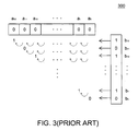
- FIG. 3 (Prior Art) is a schematic illustration showing the conventional method for storing data to the register by way of rotation. As shown in FIG. 3 , if the receiving terminal receives thirteen data bits as one data byte, the register 300 is a thirteen-bit register and the initial value of the register 300 is (0 0 0...0 0) 2 , for example.
- the thirteen data bits are sequentially stored to corresponding positions of the register 300 by way of rotation.
- the bit b 12 is stored to the memory cell a 0 .
- the bit b 12 stored to the memory cell a 0 is shifted to the memory cell a 1 to complete a first rotation operation.
- the bit b 12 stored to the memory cell a 1 is shifted to the memory cell a 2 to complete a second rotation operation.
- step 240 the receiving terminal determines whether the storing operation finishes after each bit is stored. If the storing operation is not finished yet, the procedure goes back to the step 220 to continue reading the subsequent bits. If the storing operation is finished, the procedure enters step 250. In the step 250, the receiving terminal decrypts the byte stored in the register and performs a corresponding process.
- the conventional method for decrypting the serial transmission signal has to push the program address to the stack in the step 220 so as to trigger the interrupt service function and jump to the sub-program, and also has to pop the program address from the stack so as to jump back to the main program.
- the processor of the receiving terminal needs a lot of system clock cycles to finish the operation of receiving one bit. Therefore, if the number of bits of the serial transmission signal increases and the transmission speed is required to be higher, the calculation loading of the processor of the receiving terminal will get higher and the efficiency of the processor will be reduced. In addition, if the number of bits of the serial transmission signal increases, the number of rotation commands to be performed in the step 230 will also increase so that the calculation loading of the processor thus get higher. Meanwhile, the cost is increased and the power consumption of the processor of the receiving terminal is increased.
- the invention is directed to a method for decrypting a serial transmission signal, in which one bit is read in one cycle of a serial clock signal without using an interrupt service function and then stored by an addition operation. Therefore, the serial transmission signal can be rapidly decrypted, the calculation loading of a processor can be decreased, and the power consumption of the processor can be lowered.
- a method for decrypting a serial transmission signal comprises the following steps. First, the serial transmission signal including a serial data signal and a serial clock signal is received. Next, m bits are sequentially read from the serial data signal according to the serial clock signal. Then, values corresponding to the m bits are generated. Afterwards, each of the values is added to a content value of a register by an addition operation to obtain an addition result, and then the content value is replaced with the addition result and the addition result is stored to the register.
- a method for decrypting a serial transmission signal applied to a receiving terminal comprises the following steps. First, the serial transmission signal including a serial data signal and a serial clock signal is received. Next, it is determined whether a logic level of the serial clock signal is equal to a default value. Then, a bit is read from the serial data signal when the logic level of the serial clock signal is equal to the default value. Afterwards, the bit is stored to a register.
- FIG. 1 (Prior Art) is a schematic illustration showing a conventional serial transmission signal.
- FIG 2 (Prior Art) is a flow chart showing a conventional method for decrypting the serial transmission signal.
- FIG. 3 (PriorArt) is a schematic illustration showing the conventional method for storing data to a register by way of rotation.
- FIG. 4 is a flow chart showing a method for decrypting a serial transmission signal according to a first embodiment of the invention.
- FIG. 5 is a flow chart showing a method for decrypting a serial transmission signal according to a second embodiment of the invention.
- FIG. 6 is a flow chart showing a method for decrypting a serial transmission signal according to a third embodiment of the invention.
- the invention provides a method for decrypting a serial transmission signal, in which one bit is read in one cycle of a serial clock signal without using an interrupt service function and then stored to a corresponding position of a register by an addition operation. Therefore, the calculation loading and the power consumption of a receiving terminal can be decreased, the serial transmission signal can be rapidly decrypted, and the cost of the receiving terminal can be decreased.
- FIG. 4 is a flow chart showing a method for decrypting a serial transmission signal according to a first embodiment of the invention. As shown in FIG. 4 , the method is applied to a receiving terminal. The receiving terminal decrypts data of each field according to a protocol of the serial transmission signal.
- This protocol may be, for example, a protocol for a serial transmission interface, such as a serial peripheral interface (SPI), an inter-integrated circuit (12C) or a universal asynchronous receiver/transmitter (UART).
- SPI serial peripheral interface
- 12C inter-integrated circuit
- UART universal asynchronous receiver/transmitter
- the serial transmission signal including a serial data signal and a serial clock signal is received.
- m bits are sequentially read from the serial data signal according to the serial clock signal, wherein m is a positive integer.
- the m bits may form, for example, an address byte or a data byte.
- the receiving terminal can read the bits from the serial data signal, based on timing pulses contained in the serial clock signal, in an edge triggered or level triggered manner.
- step 430 values corresponding to the m bits are sequentially generated, and an addition result is generated by performing an addition operation for the m values and then stored to a register.
- the addition operation is performed for the m values.
- the addition operation is an arithmetic addition (ADD) operation. It is assumed that the m bits of the first field are sequentially b m-1 , b m-2 ... b 1 and b 0 .
- b m-1 is equal to logic 1
- the value of 2 m-1 is added to a content value stored in the register by the arithmetic addition operation.
- the values of b m-2 ... b 1 and b 0 are equal to the logic 1
- the values of 2 m-2 ..., 2 1 and 2 0 are respectively added to the content value stored in the register by the arithmetic addition operation.
- the m bits may also be stored by way of a logic AND operation.
- the addition operation is a logic AND operation.
- b m-1 is equal to logic 1
- the value of (1 0 0...0 0) 2 is added to a content value stored in the register by the AND addition operation.
- the values of the b m-2 ...b 1 and b 0 are equal to logic 1
- the values of (0 1 0...0 0) 2 , (0 0 1...0 0) 2 , ... (0 0 0...1 0) 2 and (0 0 0...0 1) 2 are respectively added to the content value stored in the register by the logic AND operation.
- the m bits can be stored to the register without multiple rotation commands, thereby decreasing the calculation loading of the receiving terminal.
- the numbers of rotations for different bits are different, the numbers of addition operations according to the present invention for different bits are the same.
- step 440 it is determined whether the m bits have been completely stored. If the bits have not been completely stored, the procedure goes back to the step 420 to continue reading the remaining bits. If the bits have been completely stored, a first acknowledging bit is outputted to a transmitting terminal in step 450.
- FIG. 5 is a flow chart showing a method for decrypting a serial transmission signal according to a second embodiment of the invention. As shown in FIG. 5 , this method is applied to a receiving terminal. The receiving terminal decrypts bit data in each field according to a protocol of the serial transmission signal. First, in step 510, the serial transmission signal including a serial data signal and a serial clock signal is received.
- step 515 it is determined whether a logic level of the serial clock signal is equal to a default value "1". Then, in step 520, when the logic level of the serial clock signal is equal to the default value "1 ", one bit is read from the serial data signal.
- the bit is, for example, one bit of an address byte or one bit of a data byte.
- the method is to read one bit from the serial data signal in one serial clock cycle at the receiving terminal without using an interrupt service function. That is, a main program of the receiving terminal has included program codes for reading the data bit from the serial data signal. The main program is executed by a processor of the receiving terminal, for example, and the frequency of a system clock signal of the processor is higher than that of the serial clock signal. Consequently, the main program can directly perform the operation of reading the serial data signal in a serial clock cycle under the control of the system clock signal. The processor can complete the operation of reading the serial data signal without executing any interrupting process.
- the method of this embodiment can omit the conventional pushing, jumping and popping operations for the program address. Therefore, the time of waiting for processing the received data can be effectively shortened so that the speed for receiving data is increased.
- both of the rising edges and the falling edges of the serial clock signal can trigger the interrupt service function in the conventional method, so the conventional method has to finish the operation of reading one bit of data between a rising edge and a neighboring falling edge of the serial clock signal. Since this embodiment needs not to perform the interrupt service function, it is unnecessary to complete the operation of reading one bit of data between a rising edge and a falling edge at one timing pulse of the serial clock signal (typically equal to one half of the serial clock cycle), like the prior art. Therefore, this embodiment only has to finish the operation of reading one bit of data in one serial clock cycle. Consequently, this embodiment has sufficient time for reading one bit of data. More particularly, the main program may further execute operations associated with a read bit in the remaining time after reading one bit during one serial clock cycle of the serial clock signal, thereby correspondingly increasing the efficiency of the receiving terminal.
- step 530 the bit is stored in the register.
- FIG. 6 is a flow chart showing a method for decrypting a serial transmission signal according to a third embodiment of the invention. As shown in FIG. 6 , this embodiment combines the features of the first and second embodiments.
- the serial transmission signal including a serial data signal and a serial clock signal is received.
- step 620 m bits are read from the serial data signal according to a logic level of the serial clock signal, wherein m is a positive integer, and one serial clock cycle corresponds to one bit.
- the m bits form an address byte or a data byte, for example.
- a receiving terminal can read one bit from the serial data signal in one serial clock cycle without triggering an interrupt service function.
- step 630 values corresponding to the m bits are sequentially generated, and an addition result is obtained by performing an arithmetic addition operation (ADD) or a logic addition operation (AND) for the m values, and then stored to a register.
- step 640 it is determined whether the m bits have been completely stored or not. If not, the procedure goes back to the step 620 to continue reading the remaining bits. If yes, a first acknowledging bit is outputted to a transmitting terminal in step 650.
- the receiving terminal in advance, sets the field of the bits of the serial data signal to be received. Therefore, the receiving terminal can read one bit of data in one serial clock cycle of the serial clock signal without using any interrupt service function, pushing command or jumping command and without waiting. In addition, it is unnecessary to finish a reading operation for one bit between a rising edge and a falling edge at one timing pulse of the serial clock signal, so the receiving terminal can further execute associated operations during the remaining time in one serial clock cycle, thereby correspondingly increasing the efficiency of the receiving terminal.
- the method for decrypting the serial transmission signal according to the invention further directly stores each received bit to one corresponding position in the register by the addition operation.
- multiple rotation commands can be omitted, the calculation loading and the power consumption of the receiving terminal can be reduced, and the serial transmission signal can be rapidly decrypted; in addition, the cost and the power loss of the receiving terminal can be decreased.
Landscapes
- Engineering & Computer Science (AREA)
- Physics & Mathematics (AREA)
- General Physics & Mathematics (AREA)
- Mathematical Analysis (AREA)
- Theoretical Computer Science (AREA)
- Pure & Applied Mathematics (AREA)
- Computational Mathematics (AREA)
- Signal Processing (AREA)
- Computer Networks & Wireless Communication (AREA)
- Computing Systems (AREA)
- Mathematical Optimization (AREA)
- General Engineering & Computer Science (AREA)
- Computer Security & Cryptography (AREA)
- Information Transfer Systems (AREA)
- Synchronisation In Digital Transmission Systems (AREA)
Applications Claiming Priority (1)
| Application Number | Priority Date | Filing Date | Title |
|---|---|---|---|
| TW096134749A TWI444021B (zh) | 2007-09-17 | 2007-09-17 | 解譯串列傳輸訊號之方法 |
Publications (3)
| Publication Number | Publication Date |
|---|---|
| EP2037622A2 true EP2037622A2 (de) | 2009-03-18 |
| EP2037622A3 EP2037622A3 (de) | 2009-08-05 |
| EP2037622B1 EP2037622B1 (de) | 2013-03-20 |
Family
ID=40158667
Family Applications (1)
| Application Number | Title | Priority Date | Filing Date |
|---|---|---|---|
| EP08164361A Ceased EP2037622B1 (de) | 2007-09-17 | 2008-09-15 | Verfahren zum Empfangen eines seriellen Übertragungssignals |
Country Status (3)
| Country | Link |
|---|---|
| US (1) | US8259943B2 (de) |
| EP (1) | EP2037622B1 (de) |
| TW (1) | TWI444021B (de) |
Families Citing this family (2)
| Publication number | Priority date | Publication date | Assignee | Title |
|---|---|---|---|---|
| US9054851B2 (en) * | 2013-03-08 | 2015-06-09 | Microchip Technology Incorporated | Dithering circuit for serial data transmission |
| TWI795901B (zh) * | 2021-09-03 | 2023-03-11 | 國立陽明交通大學 | 具內建測試功能之串列傳輸系統 |
Family Cites Families (32)
| Publication number | Priority date | Publication date | Assignee | Title |
|---|---|---|---|---|
| US3757261A (en) * | 1972-02-11 | 1973-09-04 | Collins Radio Co | Integration and filtration circuit apparatus |
| US4023019A (en) * | 1974-09-23 | 1977-05-10 | The United States Of America As Represented By The Secretary Of The Navy | Automatic scaled digital integrator |
| US4246642A (en) * | 1979-01-22 | 1981-01-20 | Ricoh Company, Ltd. | Leaky digital integrator |
| FR2454136B1 (fr) | 1979-04-12 | 1985-12-06 | Materiel Telephonique | Additionneur sequentiel rapide |
| JPS59180871A (ja) * | 1983-03-31 | 1984-10-15 | Fujitsu Ltd | 半導体メモリ装置 |
| US4747139A (en) * | 1984-08-27 | 1988-05-24 | Taaffe James L | Software security method and systems |
| US4841466A (en) * | 1987-08-24 | 1989-06-20 | Rca Licensing Corporation | Bit-serial integrator circuitry |
| JP2778222B2 (ja) * | 1990-08-15 | 1998-07-23 | 日本電気株式会社 | 半導体集積回路装置 |
| US5440702A (en) * | 1992-10-16 | 1995-08-08 | Delco Electronics Corporation | Data processing system with condition code architecture for executing single instruction range checking and limiting operations |
| US5313469A (en) * | 1993-06-11 | 1994-05-17 | Northern Telecom Limited | Self-testable digital integrator |
| US5621901A (en) * | 1994-10-31 | 1997-04-15 | Intel Corporation | Method and apparatus for serial bus elements of an hierarchical serial bus assembly to electrically represent data and control states to each other |
| US5742847A (en) * | 1994-10-31 | 1998-04-21 | Intel Corporation | M&A for dynamically generating and maintaining frame based polling schedules for polling isochronous and asynchronous functions that guaranty latencies and bandwidths to the isochronous functions |
| US5623610A (en) * | 1994-10-31 | 1997-04-22 | Intel Corporation | System for assigning geographical addresses in a hierarchical serial bus by enabling upstream port and selectively enabling disabled ports at power on/reset |
| GB2308533B (en) * | 1994-10-31 | 1999-04-07 | Intel Corp | M & A for exchanging data, status, and commands over a hierarchical |
| KR0184136B1 (ko) * | 1996-06-03 | 1999-05-15 | 구자홍 | 범용 마이컴을 이용한 아이 스퀘어 씨 통신 장치 |
| US6282558B1 (en) * | 1997-12-19 | 2001-08-28 | Matsushita Electric Industrial Co., Ltd. | Data processing system and register file |
| ATE382897T1 (de) * | 2000-01-18 | 2008-01-15 | Infineon Technologies Ag | Mikroprozessoranordnung und verfahren zum betreiben einer mikroprozessoranordnung |
| KR100389922B1 (ko) * | 2001-01-15 | 2003-07-04 | 삼성전자주식회사 | 1000베이스-t 표준을 이용하는 기가비트 이더넷에서의고속 링크를 위한 자동-교섭 방법 및 이를 수행하기 위한장치 |
| US6915335B1 (en) | 2001-09-17 | 2005-07-05 | Cisco Technology, Inc. | Serial protocol for efficient messaging between host and intelligent daughtercards over a serial link |
| KR100513598B1 (ko) | 2002-11-27 | 2005-09-09 | 한국전자통신연구원 | 스마트 안테나 수신 시스템에서의 적응 빔형성을 위한정규화 장치 |
| US20040120516A1 (en) * | 2002-12-23 | 2004-06-24 | International Business Machines Corporation | Modular reduction method which recognizes special conditions |
| TWI243993B (en) * | 2003-08-29 | 2005-11-21 | Ali Corp | Protection method for DVD player/recorder against copy |
| WO2005039076A1 (ja) * | 2003-10-17 | 2005-04-28 | Olympus Corporation | 情報取得装置、情報提供装置、及び情報提供システム |
| US7373523B1 (en) * | 2004-04-23 | 2008-05-13 | The United States Of America As Represented By The Secretary Of The Navy | Preparing data for storage in a secure fashion |
| DE102004035843B4 (de) * | 2004-07-23 | 2010-04-15 | Infineon Technologies Ag | Router-Netzwerkprozessor |
| US7441060B2 (en) * | 2004-10-29 | 2008-10-21 | International Business Machines Corporation | System, method and storage medium for providing a service interface to a memory system |
| WO2006064738A1 (ja) * | 2004-12-14 | 2006-06-22 | Matsushita Electric Industrial Co., Ltd. | 管理サーバ装置、コンテンツ再生装置及び記録媒体 |
| JP4714482B2 (ja) * | 2005-02-28 | 2011-06-29 | 株式会社日立製作所 | 暗号通信システムおよび方法 |
| KR100871221B1 (ko) * | 2005-11-11 | 2008-12-01 | 삼성전자주식회사 | 선형 궤환 시프트 레지스터를 이용하는 통신 시스템에서부호 생성 방법 및 장치 |
| TWI338842B (en) * | 2007-03-23 | 2011-03-11 | Qisda Corp | Signal transfer systems and methods |
| US7681078B2 (en) * | 2007-05-18 | 2010-03-16 | Freescale Semiconductor, Inc. | Debugging a processor through a reset event |
| US7673338B1 (en) * | 2007-07-26 | 2010-03-02 | Dj Inventions, Llc | Intelligent electronic cryptographic module |
-
2007
- 2007-09-17 TW TW096134749A patent/TWI444021B/zh not_active IP Right Cessation
-
2008
- 2008-09-08 US US12/206,055 patent/US8259943B2/en not_active Expired - Fee Related
- 2008-09-15 EP EP08164361A patent/EP2037622B1/de not_active Ceased
Non-Patent Citations (1)
| Title |
|---|
| None |
Also Published As
| Publication number | Publication date |
|---|---|
| TWI444021B (zh) | 2014-07-01 |
| US20090074186A1 (en) | 2009-03-19 |
| TW200915797A (en) | 2009-04-01 |
| EP2037622A3 (de) | 2009-08-05 |
| EP2037622B1 (de) | 2013-03-20 |
| US8259943B2 (en) | 2012-09-04 |
Similar Documents
| Publication | Publication Date | Title |
|---|---|---|
| US9166625B2 (en) | Circuits, integrated circuits, and methods for interleaved parity computation | |
| US9075925B2 (en) | Serial peripheral interface and method for data transmission | |
| TW200935234A (en) | System and method for setting access and modification for synchronous serial interface NAND | |
| US8082435B2 (en) | Memory device initiate and terminate boot commands | |
| TW200839571A (en) | Device and method for access time reduction by speculatively decoding non-memory read commands on a serial interface | |
| CN107797821B (zh) | 重试读取方法以及使用该方法的装置 | |
| US5361371A (en) | Microprocessor with reset execution from an arbitrary address | |
| US8259943B2 (en) | Method for decrypting serial transmission signal | |
| US9170601B2 (en) | Command decoding method and circuit of the same | |
| US7734904B2 (en) | Resetting a system in response to changes of component settings | |
| US5537660A (en) | Microcontroller having selectable bus timing modes based on primary and secondary clocks for controlling the exchange of data with memory | |
| WO2019070361A1 (en) | MULTI-LINE BUS WITH DYNAMIC ADJUSTMENT SHARED BY MULTIPROTOCOL DEVICES | |
| US4975839A (en) | Instruction decode method and arrangement suitable for a decoder of microprocessors | |
| US7345496B2 (en) | Semiconductor apparatus and test execution method for semiconductor apparatus | |
| JP5251353B2 (ja) | 情報処理装置 | |
| CN1301460C (zh) | 程序状态寄存器处理状态改变的系统与方法 | |
| US7661011B2 (en) | Method and apparatus for a variable processing period in an integrated circuit | |
| US5988872A (en) | Sector data decoding method and circuit in a CD-ROM drive | |
| JPH08235073A (ja) | マイクロコンピュータ | |
| JP3958239B2 (ja) | マイクロコントローラ | |
| US20070010988A1 (en) | Emulator and emulating method | |
| US6850561B1 (en) | Predictable updating of a baud divisor of an asynchronous serial port during data reception | |
| KR100341947B1 (ko) | 모듈러 칩 선택제어회로 및 이와 관계된 회로 및 방법 | |
| CN101436167A (zh) | 解译串列传输信号的方法 | |
| US20030093651A1 (en) | Instruction sets and compilers |
Legal Events
| Date | Code | Title | Description |
|---|---|---|---|
| PUAI | Public reference made under article 153(3) epc to a published international application that has entered the european phase |
Free format text: ORIGINAL CODE: 0009012 |
|
| AK | Designated contracting states |
Kind code of ref document: A2 Designated state(s): AT BE BG CH CY CZ DE DK EE ES FI FR GB GR HR HU IE IS IT LI LT LU LV MC MT NL NO PL PT RO SE SI SK TR |
|
| AX | Request for extension of the european patent |
Extension state: AL BA MK RS |
|
| PUAL | Search report despatched |
Free format text: ORIGINAL CODE: 0009013 |
|
| AK | Designated contracting states |
Kind code of ref document: A3 Designated state(s): AT BE BG CH CY CZ DE DK EE ES FI FR GB GR HR HU IE IS IT LI LT LU LV MC MT NL NO PL PT RO SE SI SK TR |
|
| AX | Request for extension of the european patent |
Extension state: AL BA MK RS |
|
| RIC1 | Information provided on ipc code assigned before grant |
Ipc: G06F 7/504 20060101ALI20090629BHEP Ipc: H04L 9/18 20060101AFI20090113BHEP |
|
| 17P | Request for examination filed |
Effective date: 20100205 |
|
| AKX | Designation fees paid |
Designated state(s): DE FR GB NL |
|
| 17Q | First examination report despatched |
Effective date: 20101206 |
|
| GRAP | Despatch of communication of intention to grant a patent |
Free format text: ORIGINAL CODE: EPIDOSNIGR1 |
|
| GRAS | Grant fee paid |
Free format text: ORIGINAL CODE: EPIDOSNIGR3 |
|
| GRAA | (expected) grant |
Free format text: ORIGINAL CODE: 0009210 |
|
| AK | Designated contracting states |
Kind code of ref document: B1 Designated state(s): DE FR GB NL |
|
| REG | Reference to a national code |
Ref country code: GB Ref legal event code: FG4D |
|
| REG | Reference to a national code |
Ref country code: DE Ref legal event code: R096 Ref document number: 602008022994 Country of ref document: DE Effective date: 20130516 |
|
| REG | Reference to a national code |
Ref country code: NL Ref legal event code: VDEP Effective date: 20130320 |
|
| PG25 | Lapsed in a contracting state [announced via postgrant information from national office to epo] |
Ref country code: NL Free format text: LAPSE BECAUSE OF FAILURE TO SUBMIT A TRANSLATION OF THE DESCRIPTION OR TO PAY THE FEE WITHIN THE PRESCRIBED TIME-LIMIT Effective date: 20130320 |
|
| PLBE | No opposition filed within time limit |
Free format text: ORIGINAL CODE: 0009261 |
|
| STAA | Information on the status of an ep patent application or granted ep patent |
Free format text: STATUS: NO OPPOSITION FILED WITHIN TIME LIMIT |
|
| 26N | No opposition filed |
Effective date: 20140102 |
|
| REG | Reference to a national code |
Ref country code: DE Ref legal event code: R097 Ref document number: 602008022994 Country of ref document: DE Effective date: 20140102 |
|
| REG | Reference to a national code |
Ref country code: FR Ref legal event code: PLFP Year of fee payment: 9 |
|
| REG | Reference to a national code |
Ref country code: FR Ref legal event code: PLFP Year of fee payment: 10 |
|
| REG | Reference to a national code |
Ref country code: FR Ref legal event code: PLFP Year of fee payment: 11 |
|
| PGFP | Annual fee paid to national office [announced via postgrant information from national office to epo] |
Ref country code: FR Payment date: 20180813 Year of fee payment: 11 Ref country code: DE Payment date: 20180904 Year of fee payment: 11 |
|
| PGFP | Annual fee paid to national office [announced via postgrant information from national office to epo] |
Ref country code: GB Payment date: 20180912 Year of fee payment: 11 |
|
| REG | Reference to a national code |
Ref country code: DE Ref legal event code: R119 Ref document number: 602008022994 Country of ref document: DE |
|
| PG25 | Lapsed in a contracting state [announced via postgrant information from national office to epo] |
Ref country code: DE Free format text: LAPSE BECAUSE OF NON-PAYMENT OF DUE FEES Effective date: 20200401 |
|
| GBPC | Gb: european patent ceased through non-payment of renewal fee |
Effective date: 20190915 |
|
| PG25 | Lapsed in a contracting state [announced via postgrant information from national office to epo] |
Ref country code: FR Free format text: LAPSE BECAUSE OF NON-PAYMENT OF DUE FEES Effective date: 20190930 Ref country code: GB Free format text: LAPSE BECAUSE OF NON-PAYMENT OF DUE FEES Effective date: 20190915 |