EP2040168A2 - Système de stockage doté d'une fonction de sauvegarde de données dans une mémoire cache - Google Patents
Système de stockage doté d'une fonction de sauvegarde de données dans une mémoire cache Download PDFInfo
- Publication number
- EP2040168A2 EP2040168A2 EP08251452A EP08251452A EP2040168A2 EP 2040168 A2 EP2040168 A2 EP 2040168A2 EP 08251452 A EP08251452 A EP 08251452A EP 08251452 A EP08251452 A EP 08251452A EP 2040168 A2 EP2040168 A2 EP 2040168A2
- Authority
- EP
- European Patent Office
- Prior art keywords
- data elements
- dirty data
- cache memory
- control module
- module
- Prior art date
- Legal status (The legal status is an assumption and is not a legal conclusion. Google has not performed a legal analysis and makes no representation as to the accuracy of the status listed.)
- Granted
Links
Images










Classifications
-
- G—PHYSICS
- G06—COMPUTING OR CALCULATING; COUNTING
- G06F—ELECTRIC DIGITAL DATA PROCESSING
- G06F11/00—Error detection; Error correction; Monitoring
- G06F11/07—Responding to the occurrence of a fault, e.g. fault tolerance
- G06F11/14—Error detection or correction of the data by redundancy in operations
- G06F11/1402—Saving, restoring, recovering or retrying
- G06F11/1415—Saving, restoring, recovering or retrying at system level
- G06F11/1441—Resetting or repowering
-
- G—PHYSICS
- G06—COMPUTING OR CALCULATING; COUNTING
- G06F—ELECTRIC DIGITAL DATA PROCESSING
- G06F12/00—Accessing, addressing or allocating within memory systems or architectures
- G06F12/02—Addressing or allocation; Relocation
- G06F12/08—Addressing or allocation; Relocation in hierarchically structured memory systems, e.g. virtual memory systems
- G06F12/0802—Addressing of a memory level in which the access to the desired data or data block requires associative addressing means, e.g. caches
- G06F12/0804—Addressing of a memory level in which the access to the desired data or data block requires associative addressing means, e.g. caches with main memory updating
-
- G—PHYSICS
- G06—COMPUTING OR CALCULATING; COUNTING
- G06F—ELECTRIC DIGITAL DATA PROCESSING
- G06F11/00—Error detection; Error correction; Monitoring
- G06F11/07—Responding to the occurrence of a fault, e.g. fault tolerance
- G06F11/16—Error detection or correction of the data by redundancy in hardware
- G06F11/20—Error detection or correction of the data by redundancy in hardware using active fault-masking, e.g. by switching out faulty elements or by switching in spare elements
- G06F11/2015—Redundant power supplies
-
- G—PHYSICS
- G06—COMPUTING OR CALCULATING; COUNTING
- G06F—ELECTRIC DIGITAL DATA PROCESSING
- G06F12/00—Accessing, addressing or allocating within memory systems or architectures
- G06F12/02—Addressing or allocation; Relocation
- G06F12/08—Addressing or allocation; Relocation in hierarchically structured memory systems, e.g. virtual memory systems
- G06F12/0802—Addressing of a memory level in which the access to the desired data or data block requires associative addressing means, e.g. caches
- G06F12/0866—Addressing of a memory level in which the access to the desired data or data block requires associative addressing means, e.g. caches for peripheral storage systems, e.g. disk cache
-
- Y—GENERAL TAGGING OF NEW TECHNOLOGICAL DEVELOPMENTS; GENERAL TAGGING OF CROSS-SECTIONAL TECHNOLOGIES SPANNING OVER SEVERAL SECTIONS OF THE IPC; TECHNICAL SUBJECTS COVERED BY FORMER USPC CROSS-REFERENCE ART COLLECTIONS [XRACs] AND DIGESTS
- Y02—TECHNOLOGIES OR APPLICATIONS FOR MITIGATION OR ADAPTATION AGAINST CLIMATE CHANGE
- Y02D—CLIMATE CHANGE MITIGATION TECHNOLOGIES IN INFORMATION AND COMMUNICATION TECHNOLOGIES [ICT], I.E. INFORMATION AND COMMUNICATION TECHNOLOGIES AIMING AT THE REDUCTION OF THEIR OWN ENERGY USE
- Y02D10/00—Energy efficient computing, e.g. low power processors, power management or thermal management
Definitions
- the present generally invention relates to the backup of data stored in a cache memory of a storage system.
- Japanese Patent Application Laid-Open No. 2002-99390 As a technology on the backup of data stored in a cache memory, a technology disclosed in Japanese Patent Application Laid-Open No. 2002-99390 , for example, is known.
- Japanese Patent Application Laid-Open No. 2002-99390 if power from the outside is shut down in a state where data, which has not yet been saved to a disk, exists in a cache memory, the data in the cache memory is copied to a non-volatile memory while a battery can supply power. After copying completes, power from the battery continues to the cache memory. When the power supply from the outside is restarted, the data stored in the cache memory is used if the power supply from the battery continues, or the data is restored from the non-volatile memory to the cache memory if the battery power has run down.
- System down time is the time from the storage system stopping acceptance of I/O commands from a host device (e.g. host computer) to restarting the system. If the end of system down time, which was started at a certain point (e.g.
- the time length required for this returning data influences the length of the system down time. Since the storage capacities of cache memories are increasing, as mentioned above, the data volume of staging increases, and staging time length increases accordingly. As a result, the system down time becomes lengthy. Generally a storage system is demanded to be operational 24 hours/365 days non-stop, so as to present no hindrance to the work of the user, therefore a lengthy system time is a problem.
- An aspect of the present invention is a storage system comprising a plurality of control modules having a plurality of cache memories respectively.
- One or more dirty data element(s), out of a plurality of dirty data elements (data elements which have not been incorporated in the storage device) stored in a first cache memory in a first control module, is/are copied to a second cache memory in a second control module.
- the one or more dirty data element(s) stored in the second cache memory is/are backed up to a non-volatile storage resource.
- the dirty data elements backed up from the first cache memory to the non-volatile storage resource are dirty data elements, other than the one or more dirty data element(s) of which copying has completed, out of the plurality of dirty data elements.
- a storage system comprises a plurality of storage devices and a plurality of control modules having a plurality of cache memories and a plurality of control units respectively.
- the storage system copies the one or more dirty data element(s) (data elements which have not be incorporated in the storage device) out of a plurality of dirty data elements stored in a first cache memory in a first control module to a second cache memory in a second control module.
- the one or more dirty data element(s) is/are backed up from the second cache memory to a non-volatile storage resource, and dirty data elements, other than the one or more dirty data element(s), are backed up from the first cache memory to the non-volatile storage resource.
- Embodiment 2 according to the Embodiment 1, one or more dirty data element(s) is/are copied to a second cache memory while power is being supplied from a primary power supply. If power is supplied from a battery after power supply from the primary power supply stops, the above mentioned backup operations are performed respectively.
- Embodiment 3 wherein if a power failure is recovered and power is supplied again after a battery runs down (e.g. power supply from the battery stopped, or discharge voltage became lower than a predetermined threshold), the dirty data elements are staged from the non-volatile storage resource to the first cache memory, and the dirty data elements are staged from the non-volatile storage resource to the second cache memory, and the dirty data elements are copied from the second cache memory to the first cache memory in parallel with the staging.
- a power failure is recovered and power is supplied again after a battery runs down (e.g. power supply from the battery stopped, or discharge voltage became lower than a predetermined threshold)
- the dirty data elements are staged from the non-volatile storage resource to the first cache memory
- the dirty data elements are staged from the non-volatile storage resource to the second cache memory
- the dirty data elements are copied from the second cache memory to the first cache memory in parallel with the staging.
- the first control module creates management information to indicate a cache area, where a dirty data element exists, of the first cache memory and to indicate a control module to which the dirty data element is copied in the control module, and writes it to the first cache memory, and updates the management information as the copying of the dirty data elements completes.
- the storage system backs up the management information in addition to the dirty data element from the first cache memory to the non-volatile storage resource, and when power supply is restarted, the management information in addition to the dirty data element are staged from the non-volatile storage resource to the first cache memory.
- the plurality of dirty data elements are evenly divided according to the total of the number of the first control modules and the number of the second control modules, with one or more provided for the first control modules.
- the dirty data element(s) acquired by this division is/are copied.
- each control unit writes data according to an I/O command from the host device to the cache memory, and writes data written in the cache memory to at least one of the plurality of storage devices, or sends the data to the host device.
- the first control unit instructs the second control unit in the second control module to copy the above mentioned one or more dirty data element(s).
- the second control unit writes the one or more dirty data element(s) to the second cache memory in response to this instruction. By this, the one or more dirty data element(s) is/are copied from the first cache memory to the second cache memory.
- the storage system further has a plurality of power supply modules, which are the power supplies of the plurality of control modules respectively.
- the number of second control modules is the number of first control modules or more, and one or more second control modules are provided for one first control module.
- the non-volatile storage resource severs as a plurality of non-volatile memory modules of a plurality of control modules respectively (e.g. a module having one or more non-volatile memory/memories).
- Each control module further has a connection unit for communicably connecting the cache memory and the control unit.
- the control modules are interconnected by the interconnection of the control units.
- the power supply module includes a battery and a primary power supply.
- the primary power supply supplies power to the cache memory and the control unit, and the battery supplies power to the cache memory and the control unit when the power from the primary power supply stops.
- the first control unit receives I/O commands from the host device while power is being supplied from the primary power supply. If the received I/O command is a write command, the first control unit writes a data element according to the write command to the first cache memory. The first control unit also creates the above mentioned management information, and writes it to the first cache memory.
- the first control unit sends an instruction, to copy one or more dirty data element(s), to the second control unit via two or more connection units including a.first connection unit of the first control module and a second connection unit of the second control module. Then if a plurality of new dirty data elements exist in the first cache memory because of a plurality of data elements according to one or more write command(s) being written in the first cache memory, the first control unit sends an instruction, to copy one or more dirty data element(s) out of the new plurality of dirty data elements, to the second control unit via two or more connection units, and updates the management information as copying of the dirty data elements completes.
- the second control unit While power is being supplied from the battery, after the power supply from the primary power supply stops, the second control unit backs up the dirty data elements written in the second cache memory, to the second non-volatile memory module of the second control module, stages the dirty data elements from the second non-volatile memory module to the second cache memory when the power supply is restarted, and sends an instruction to copy the staged dirty data elements to the first control unit via two or more connection units in parallel with the staging.
- the first control unit While power is being supplied from the battery after the power supply from the primary power supply stops, the first control unit backs up the dirty data elements, other than the one or more dirty data element(s) of which copying has completed, and the management information from the first cache memory to the first non-volatile memory module of the first control module, stages the management information and the dirty data elements from the first non-volatile memory module to the first cache memory when the power supply from the primary power supply is restarted, and writes the dirty data elements staged in the second cache memory in the first cache memory. Then the first control unit integrates the dirty data elements written in the first cache memory and the staged dirty data elements, for example.
- the first control unit sends an instruction to copy to the second control module while receiving the power from the primary power supply, and if the power from the primary power supply stops and power is received from the battery, the first control module backs up the dirty data elements from the first cache memory to the non-volatile storage resource without sending an instruction for copying.
- control modules are interconnected by the interconnection of the connection units.
- Embodiment 11 when a write command is received from the host device, and if the consumption ratio of the first cache memory is a third predetermined ratio or more, the first control unit sends one or more data element(s) according to the write command to another control module (via two or more connection units, including a connection unit in another control module and the first connection unit), for example, and this other control module writes the one or more data element(s) to a cache memory in this other control module.
- Embodiment 12 In Embodiment 12 according to at least one of Embodiments 1 to 11, two or more storage devices, out of the plurality of storage devices, are assigned to each control module respectively. Each logic volume is formed based on two or more storage devices, and each logical volume is a logical volume assigned to each control module.
- the first control unit receives a write command from the host device and if the open status of the assigned logical volume for the first control unit itself, specified by the write command, is worse than a predetermined status, then the first control unit sends one or more data element(s) according to the write command to another control module (via two or more connection units including a connection unit in this other control module and the first connection unit), for example.
- This other control module writes the one or more data element(s) to a cache memory of this control module, and writes the one or more data element(s) written in the cache memory to a logical volume assigned to this control module.
- Embodiment 13 if a new plurality of dirty data elements exist in the first cache memory because a plurality of data elements according to one or more write commands are written in the first cache memory after the instruction to copy one or more dirty data element(s) is/are sent, the first control unit sends an instruction to copy one or more dirty data element(s) out of the plurality of new dirty data elements to the second control module.
- the second control unit backs up the dirty data elements copied in the second cache memory to the non-volatile storage resource, stages the dirty data elements from the non-volatile storage resource to the second cache memory, and sends an instruction to copy the staged dirty data elements to the first control module in parallel with the staging.
- the first control unit stages the management information and dirty data elements from the non-volatile storage resource to the first cache memory, and writes the dirty data elements from the second control module to the first cache memory responding to the instruction of copying.
- the data stored in a plurality of physical or logical storage areas (e.g. segments) constituting the cache memory respectively, that is, the data stored in one storage area, is called a "data element".
- a data element For example, if write data according to one write command is written to a cache memory, one or more write data element(s) constituting the write data exist(s) in the cache memory.
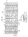
- Fig. 1A shows an external front face of a storage system according to an embodiment of the present invention.
- the storage system 100 is comprised of a plurality of module packages.
- the module package includes a power supply module for supplying power to predetermined composing elements in this module package, and is installed in a body 101 which can mount three (three or more, or less is acceptable) module packages.
- Examples of the module package is DKU (DisK Unit) module package 105 and DKC (DisK Controller) module package 111.
- DKU DisK Unit
- DKC DisK Controller
- the body 101 only DKU module packages 105 may be mounted or only DKC module packages 111 may be mounted, or both DKU module packages 105 and DKC module packages 111 may be mounted.
- the mounting location on the body 101 and the kind of modules to be mounted may be defined in advance, or may be undefined.
- the DKU module package 105 has two DKU modules 107 and one power supply module 109, for example.
- the DKU module 107 includes a plurality of disk devices.
- the drive of a hard disk or non-volatile disk type storage media, such as DVD (Digital Versatile Disk) is used (this is not limited to a disk type storage media, but a drive of another type of storage media, such as a non-volatile semiconductor memory (e.g. flash memory) may be used).
- a RAID group is formed by two or more disk devices out of the plurality of disk devices. Based on the storage space of a RAID group, one or more logical storage device(s) (hereafter called "LDEV”) is/are formed.
- the LDEV can be called a logical volume or a logical unit.
- the power supply module 109 will be described later.
- the DKC module package 111 has a DKC module 113 and a power supply module 115.
- the DKC module 113 will be described later.
- the power supply module 115 includes, as Fig. 1B shows, an AC/DC power supply (primary power supply) 116 for converting AC power from an external power supply (e.g. commercial power supply) into DC power and supplying it, and a battery (secondary power supply) 118 for supplying DC power to predetermined composing elements instead of the AC/DC power supply 116 when the supply of DC power from the AC/DC power supply 116 stops, due to a power failure, for example.
- an AC/DC power supply primary power supply
- a battery secondary power supply
- the AC/DC power supply 116 supplies power to individual composing elements (later mentioned FE-PK, BE-PK, MP-PK and CM-PK) in the DKC module 113 in the DKC module package 111 including this AC/DC power supply 111.
- the battery 118 supplies power to at least elements that require backup (e.g. CM-PK and SSD) for the dirty data elements (data elements not yet written in the disk device) from the CM (cache memory) to SSD, of the DKC module 113 in the DKC module package 111 including the battery 118.
- a power supply module 109 in the DKU module package 105 has only an AC/DC power supply for supplying DC power to each disk device, and does not have a battery, unlike the power supply module 115.
- DKU modules 107 For each DKC module 113, assigned DKU modules 107, that is, the DKU modules 107 connected to a later mentioned BE-PK in the DKC module 113, are defined in advance.
- DKC modules 113 there are four DKC modules 113 (hereafter referred to by serial numbers 1, 2, 3 and 4 for convenience), and the DKU module 107 in the range enclosed by the dotted line H1 is assigned to the DKC module 1, the DKU module 107 in the range enclosed by the dotted line H2 is assigned to the DKC module 2, the DKU module 107 enclosed by the dotted line H3 is assigned to the DKC module 3, and the DKU module 107 enclosed by the dotted line H4 is assigned to the DKC module 4.
- the DKC modules 1 to 4 can also access the DKU modules assigned to other DKC module 1 to 4 respectively. Details will be described later.
- the number of DKC modules 113 may be more or less than 4.
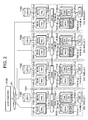
- Fig. 2 shows the configuration of the four DKC modules 1 to 4 and the relationship thereof.
- the configurations of the DKC modules 1 to 4 are virtually the same. Each configuration of the DKC module 1 to 4 will now be described using DKC module 1 as an example.
- the reference number of a composing element in a DKC module is assigned by a primary number and a serial number of the DKC module, and this combination of primary number and serial number is used in the description if the same type of composing elements are distinguished, and only a primary number is used if the same type of composing elements are not distinguished.
- the primary number 1151 is used to indicate an FE-PK of a DKC module
- 1151-1 is used to indicate the FE-PK of the DKC module 1
- 1151-2 is used to indicate the FE-PK in the DKC module 2.
- LDEVs 1 to 4 are formed using the DKU module 107 assigned to the DKC modules 1 to 4 respectively. Therefore it is assumed that LDEV 1 is assigned to the DKC module 1, LDEV 2 is assigned to the DKC module 2, LDEV 3 is assigned to the DKC module 3, and LDEV 4 is assigned to the DKC module 4.
- the DKC module 1 has FE-PK (Front End - Package) 1151-1, BE-PK (Back End - Package) 1153-1, MP-PK (MicroProcessor - Package) 1137-1, CM-PK (Cache Memory - Package) 1143, SSD (Solid State Device) 1151-1 and SW-PK (Switch - Package) 1135-1. These composing elements are duplicated respectively.
- the FE-PK 1151-1 is a circuit board for controlling communication with a host computer 1100, such as receiving from the host computer 1100 I/O commands (write command/read command) via a communication network 171 or sending read data (data according to a read command) to the host computer 1100.
- the FE-PK 1151-1 has a protocol chip ("PRC" in Fig. 2 ) 1131-1 for performing protocol conversion processing in communication with the host computer 1100.
- PRC protocol chip
- the FE-PK 1151-1 notifies the reception of the I/O command to a first MP (MicroProcessor) 1141A-1 in the MP-PK 1137-1 via an SW-PK 1135-1.
- the FE-PK 1151-1 stores the data according to the write command (hereafter "write data") to a storage resource (e.g. memory), which is not illustrated, in the FE-PK 1151-1.
- a storage resource e.g. memory
- the MP-PK 1137-1 is a circuit board which has a first MP 1141A-1 for performing front end processing (processing for the host computer 1100), a second MP 1141B-1 for performing back end processing (processing for LDEV), and an MCH (Memory Controller Hub) 1139-1 for connecting the first MP 1141A-1 and the second MP 1141B-1.
- the first MP 1141A-1 receives notice about reception of a write command from the FE-PK 1151-1, acquires the write data from the host computer 1100 via the FE-PK 1139-1, and writes the acquired write data to CM 1147-1, for example.
- the first MP 1141A-1 receives a notice about reception of a read command from the FE-PK 1151-1, checks whether the target read data exists in a CM 1147-1, reads the read data from the CM 1147-1 if it exists, and sends it to the FE-PK 1139-1 (that is, sends it to the host computer 1100 via the FE-PK 1139-1), or has a second MP 1141B-1 read a read data from the LDEV 1 if it does not exist, reads the read data, which was read and stored in the CM 1147-1, from the CM 1147-1, and sends it to the host computer 1100 via the FE-PK 1139-1, for example.
- the second MP 1141B-1 reads write data from the CM 1147-1, and sends this write data and information to indicate a write destination thereof (e.g. disk device corresponding to the LDEV 1 and write destination address thereof) to the BE-PK 1153-1 (that is, writes the write data to the LDEV 1 via the BE-PK 1153), or reads read data from the LDEV 1 via the BE-PK 1153-1 and writes it to the CM 1147-1.
- a write destination thereof e.g. disk device corresponding to the LDEV 1 and write destination address thereof
- the BE-PK 1153-1 is a circuit board for controlling communication with each disk device connected to the BE-PK 1153-1, such as writing write data, which the second MP 1141B-1 read from the CM 1147-1, to the LDEV 1, or reading read data from the LDEV 1.
- the BE-PK 1153-1 has a protocol chip ("PRC" in Fig. 2 ) 1133-1 for performing protocol conversion processing in communication with a disk device.
- the CM-PK 1143-1 is a circuit board having a CM (Cache Memory) 1147-1, which is a volatile memory, and a CMA (Cache Memory Adapter) 1145-1, which is an interface for reading or writing data from/to the CM 1147-1.
- CM Cache Memory
- CMA Cache Memory Adapter
- the SSD is a composite module having a plurality of non-volatile memories (e.g. a plurality of flash memories).
- the SW-PK 1136-1 is a switch circuit board for controlling communication among the FE-PK 1151-1, BE-PK 1153-1, MP-PK 1137-1 and CM-PK 1143.
- the FE-PK 1151-1, BE-PK 1153-1, MP-PK 1137-1 and CM-PK 1143 are connected to the SW-PK 1136-1.
- the SW-PK 1136-1 is also connected with an SW-PK 1136 of another DKC module via a link (e.g. cable) 1161.
- the DKC module 1 is connected so as to exchange data with other DKC modules 2 to 4.
- the DKC modules may be interconnected by the interconnection of FE-PKs, but the interconnection of SW-PKs is used in the present embodiment, as mentioned above.
- SW-PK 1135-1 to 1135-4 are connected to all the other SW-PKs respectively. Because of this, no matter which DKC module 113 uses a CM 1147 of any other DKC module 113 or LDEV 1155 assigned to any other DKC module 113, the DKC module 113 can send via a link 1161 or another SW-PK1135 an instruction to the MP-PK 1137 in another DKC module 113 to which CM 1147 to be used or LDEV 1155 to be used is assigned.
- the MP-PK 1137-1 judges whether the consumption ratio of the LDEV 1 (ratio of consumed storage capacity to the storage capacity of LDEV 1) exceeds a first threshold, and/or the consumption ratio of the CM 1147-1 (ratio of total amount of dirty data elements to the storage capacity of the CM 1147-1) exceeds a second threshold (S2501). If it is judged that the consumption ratio of the LDEV 1 does not exceed the first threshold and/or the consumption ratio of the CM
- the MP-PK 1137-1 writes the write data according to the write command to the CM 1147-1 (S2502), reads this write data from the CM 1147-1, and writes it to the LDEV 1 (S2503). If it is judged that the consumption ratio of the LDEV 1 exceeds the first threshold and/or the consumption ratio of the CM 1147-1 exceeds the second threshold (YES in S2501), then the MP-PK 1137-1 transfers the write command to another DKC module (e.g. DKC module 2), and records the transfer of the address specified by the received write command (e.g. ID of LDEV or LBA (Logical Block Address)) to another DKC module (e.g.
- DKC module 2 in a transfer management information (information to indicate a DKC module to which an address data is transferred, and information stored in a memory in the MP-PK 1137-1, for example) (S2504).
- the consumption ratio of the assigned LDEV is the first threshold or less
- the consumption ratio of the CM is the second threshold or less, and this information can be known by the MP-PK
- the MP-PK in the other DKC module which received the CM write command writes the write data according to the received write command to the CM (S2511), and writes this write data to the assigned LDEV (S2512).
- the MP-PK in the other DKC module writes an address management information to indicate the address of the write data and the write destination thereof to the storage resource in this other DKC module.
- the MP-PK 1137-1 of the DKC module 1 waits until the consumption ratio of the LDEV 1 becomes the first threshold or less, and or the consumption ratio of the CM 1147-1 becomes the second threshold or less (YES in S2505, and S2506), and if the consumption ratio of the LDEV 1 becomes the first threshold or less and/or the consumption ratio of the CM 1147-1 becomes the second threshold or less (NO in S2505), the MP-PK 1137-1 acquires the write data from the other DKC module at the transfer destination based on the transfer management information (S2507), and performs processing after S2502.
- the MP-PK 1137-1 can acquire the transferred write data by notifying the acquired address of the write data to the other DKC module and the MP-PK in the other DKC module referring to the address management information, acquiring the write data from the location corresponding to the notified address and transferring it to the DKC module 1.
- the MP-PK 1137-1 judges whether the read data, which is supposed to exist in an address specified by the read command, exists in another DKC module by referring to the transfer management information (S2601).
- the MP-PK 1137-1 sends the read data in the CM 1147-1 to the host (S2605) if this read data remains in the CM 1147-1 (YES in S2602), and if this read data does not remain in the CM 1147-1 (NO in S2602), the MP-PK 1137-1 reads the read data from the specified address (block in LDEV 1), and writes it in the CM 1147-1 (S2603 and S2604), and sends the read data in the CM 1147-1 to the host (S2605). If it is judged that the read data is in another DKC module (e.g.
- the MP-PK 1137-1 acquires the read data from the other DKC module (S2606), and performs processing in S2604 and later.
- the MP-PK 1137-1 notifies the address specified by the read command to the other DKC module
- the MP-PK in the other DKC module refers to the address management information, reads the read data from a location corresponding to the notified address (reads the read data from the CM if it remains in the CM, or reads the read data from the assigned LDEV and writes it to the CM, and reads this read data from the CM if the read data does not remain in the CM), and transfers the read data to the DKC module 1, then the MP-PK 1137-1 can acquire the read data from the other DKC module.
- SW-PKs 1135 is not limited to the example in Fig. 4B , but one SW-PK 1135 may be connected with at least one other SW-PK 1135.
- a DKC module 113 may use the CM 1147, or the assigned LDEV 1155 of the other DKC module 113 via a plurality of links 1161 and plurality of SW-PKs 1135.
- the SW-PK 1135-1 and the SW-PK 1135-3 do not have to be interconnected.
- the CM 1135-3 connected to the SW-PK 1135-3 can be used via the SW-PK 1135-2.
- the coupling between PKs (packages) of the FE-PK 1151, BE-PK 1153, MP-PK 1137 and CM-PK 1143 implemented by the SW-PK 1135 may be called a "close coupling", and the coupling between the SW-PKs 1135 may be called a "loose coupling”.
- the data exchange between PKs within one DKC module 113 which is performed via the SW-PK 1135 and not via a coupling between the SW-PKs 1135 (link 1161), can be performed at high-speed, and the data exchange between DKC modules 113, which is performed not only via the SW-PK 1135 but also via a coupling between the SW-PKs 1135, is slower than the data transfer speed within the DKC module 113.
- close coupling refers to a coupling with which the data transfer speed is fast (that is, coupling implemented by the SW-PK 1135), and loose coupling refers to a coupling with which the data transfer speed is slower (that is, coupling implemented by the link 1161).
- each DKC module 113 can mount the SSD 1151-1 to 1151-4 and dirty data elements in the CM 1147 can be copied between the DKC modules 113, as mentioned above. There are some possible cases where this copying is performed, and the following (case A) and (case B) are examples.
- (Case A) is generated by the following causes, for example.
- the second MP 1141B-1 refers to the management information group 200, and specifies a cache area where dirty data elements which require backup are stored, and saves the dirty data elements existing in the specified cache area to the SSD 1151-1 (copy) (S1301).
- the second MP 1141B-1 judges whether the discharge voltage (DC voltage) from the battery 118 in the power supply module 115, corresponding to the DKC module 1, is a predetermined value or less.
- the discharge voltage of predetermined value or less means that the power stored in the battery 118 is exhausted.
- the second MP 1141B-1 can release the saved dirty data elements from the SSD 1151-1 (S1303), since the saved dirty data elements remain in the CM 1147-1 due to the power supply from the battery 118. In other words, it is unnecessary to return the dirty data elements from the SSD 1151-1 to the CM 1147-1. Releasing the dirty data elements may mean to erase the dirty data elements or to hold information to allow overwriting other data elements on the dirty data elements.
- the second MP 1141B-1 decides to stage the management information group 200 from the SSD 1151-1 to the CM 1147-1 (S1501).
- the area of the SSD 1151-1, where the management information group 200 exists, can be specified by predetermining the storage destination of the management information group 200 in the SSD 1151-1, for example.
- the second MP 1141B-1 also decides to return (restore) the dirty data elements from the SSD 1151-1 to the CM 1147-1 (S1502).
- the second MP 1141B-1 reads the data elements constituting the management information group 200 from the SSD 1151-1 until reading the management information group 200 to the CM 1147-1 completes (NO in 1503, and S1504).
- the second MP 1141B-1 repeats reading of the dirty data elements from the SSD 1151-1 and writing the dirty data elements to the CM 1147-1 until staging all the saved dirty data elements to the CM 1147-1 completes (NO in S1505, and S1506).
- the staging of all the dirty data elements completes (YES in S1505), the processing ends.
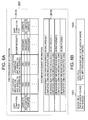
- the configuration example of the dirty data elements stored in the SSD 1151-1 is shown in Fig. 6B .
- the second MP 1141B-1 which performs the saving, adds a header field 1501 to a data field 1503 where the dirty data elements are stored, and an ID of the transmission source DKC module is recorded in the header field 1501, and an address of the saving source cache area is recorded in the data field 1503.
- the dirty data elements read from the SSD 1151-1 are staged in the saving source cache area, which is specified by the dirty data elements.
- a power failure occurrence when S1402 is YES in Fig. 14 indicates that a failure occurred in the management information group 200 after backup necessity of the copied dirty data element is updated to "backup unnecessary" (after S1207). Therefore the processing in S1601 or later in Fig. 16 is performed.
- the respective second MP 1141B-1 to 1141B-4 refers to the management information group 200 or the cache management information in each DKC module 1 to 4, and specifies a cache area where the dirty data elements which require backup are stored, and saves the dirty data elements, existing in the specified cache area, to the SSD 1151-1 to 1151-4 respectively (copy) (S1601).
- the second MP 1141B-1 updates the second management information 200 (e.g. updates the saving completion flag corresponding to each copied dirty data element from information to indicate incomplete to information to indicate complete). If power returns after this (YES in S1606), the processing advances to S1603, and if power does not return (NO in S1606), the processing advances to S1607.
- the second MP 1141B-1 to 1141B-4 judge whether the discharge voltage (DC voltage), from the battery 118 in the power supply module 115 corresponding to each DKC module 1 to 4, is a predetermined value or less. If power returns before the discharge voltage becomes a predetermined value or less (NO in S1607 and YES in S1606), the saved dirty data elements remain in the CM 1147-1 to 1147-4 because of power supply from the battery 118, so the second MP 1141B-1 to 1141B-4 may release the saved dirty data elements from the SSD 1151-1 to 1151-4 (S1603). In other words, it is unnecessary to return the dirty data elements from the SSD 1151-1 to 1151-4 to the CM 1147-1 to 1147-4.
- the second MP 1141B-1 decides to stage the management information group 200 from the SSD 1151-1 to the CM 1147-1 (S1701).
- the second MP 1141B-1 to 1141B-4 also decide to return (restore) the dirty data elements from the SSD 1151-1 to 1151-4 to the CM 1147-1 to 1147-4 (S1702).
- the second MP 1141B-2 to 1141B-4 decide to transfer the staged dirty data elements from the CM 1147-2 to 1147-4 to the CM 1147-1 (S1703).
- the second MP 1141B-1 decides to perform integration and restoration processing for the dirty data elements transferred from the slave DKC modules 2 to 4 (S1705).
- the second MP 1141B-1 to 1141B-4 repeats reading of dirty data elements from the SSD 1151-1 to 1151-4, and writing these dirty data elements to the CM 1147-1 to 1147-4 (NO in S1706 and S1707).
- S1708 is performed.
- the dirty data elements read from the SSD 1151-1 to 1151-4, are staged in the saving source cache areas specified by the dirty data elements respectively (dotted lines R1 to R4 in Fig. 8B ).
- the second MPs 1141B-2 to 1141B-4 repeat transfer of the dirty data elements from the CM 1147-2 to 1147-4 (NO in S1708, and S1709).
- S1710 is executed.
- Each dirty data element staged in the CM 1147-2 to 1147-4 specifies that the copy source DKC module is the DKC module 1, so the plurality of dirty data elements staged in the CM 1147-2 to 1147-4 are collected in the CM 1147-1 in the DKC module 1.
- a dirty data element in the CM 1147-2 to 1147-4 is written in the cache area in the CM 1147-1 corresponding to the cache area where the dirty data element is stored (dotted line T2 to T4 in Fig. 8B ).
- the dirty data element staged in the cache area #1 in the CM 1147-2 is written to the cache area #1 in the CM 1147-1.
- the DKC module 1 refers to the copy source information and copy destination information of each cache area (e.g. segment) in the first management information 201A of the management information group (see Fig. 6A ). (The management information group has been staged in the CM of the DKC module 1 in S1704 in Fig. 17 ).
- the DKC module 1 issues a job to copy the data elements in the copy destination cache area, to the CM of the original DKC module 1, to each DKC module 2, 3 and 4 based on the above mentioned copy destination information/copy source information (the destination to which a copied data element is returned (cache address) need not be the same as the original cache address).
- the above mentioned job management information is stored in the second management information 201B of the management information group in the DKC module 1 (see Fig. 6A ), and the management information group is updated each time copy processing for each cache area completes.
- the second MP 1141B-1 releases the management information group 200 (S1712).
- the management information group related to the dirty data division is released (e.g. deleted).
- the storage system 100 becomes ready status (status where the receiving of I/O commands can be started) (S1713). Ready status occurs when all the following conditions are satisfied.
- Staging processing of the dirty data elements from the SSD to the CM has been completed.
- Configuration information (information on the configuration of the storage system 100, such as information on a RAID where an LDEV exists) is read from the memory in the CM-PK, and is staged in the CM.
- Power ON processing processing executed when power is turned ON, such as boot processing) of the MP in the MP-PK has been completed.
- Disk device has been started and is in a status to receive I/O commands (in other words, the disk device is in ready status).
- a predetermined diagnosis was performed between composing elements (e.g. diagnosis program was executed), and completed without detecting error(s).
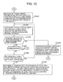
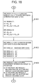
- the second MP 1141B-1 judges whether there are two DKC modules of which the consumption ratio is the first predetermined ratio or more, including the DKC module 1 (S1102). If the judgment result is "not 2" (the judgment result is "3" or "4") (NO in S1102), then the number of DKC modules to be a copy designation of a dirty data element is 1 or 0 (e.g.
- the processing returns to S1100. If the judgment result is "2" (YES in S1102), then the second MP 1141B-1 judges whether the consumption ratios of the CM 1147 of the rest of the DKC modules 113 are all less than the second predetermined ratio (S1103).
- the processing returns to S1100, and if it is judged that all the consumption ratios of all the CMs 1147 are less than the second predetermined ratio (YES in S1103), then the processing advances to S1801 in Fig. 18 .
- the processing after S1801 is the processing which is executed in the case of (case B).
- the second MP 1141B-x (and 1141B-y) evenly divides the dirty data element group in the CM 1147-x (and 1147-y) into two.
- the dirty data element group in the CM 1147-1 is divided in the following first and second initial dirty sub-groups (initial dirty sub-groups A1' and A2'), and the dirty data element group in the CM 1147-2 is divided into the following third and fourth initial dirty sub-groups (initial dirty sub-groups A3' and A4').
- the second MP 1141B-1 assigns the initial dirty sub-groups A1' and A2' to the DKC modules 1 and 3 respectively (the second MP 1141B-2 assigns the initial dirty sub-groups A3' and A4' to the DKC modules 2 and 4 respectively).
- the result of the assignment is as shown in the drawing.
- the management information group generated by the DKC module 1 is called the "management information group 200-1"
- the management information group generated by the DKC module 2 is called the "management information group 200-2".
- the second MP 1141B-1 (and 1141B-2) stores the management information group 200-1 (and 200-2) to the CM 1147-1 (and 1147-2).
- Fig. 9A shows, two initial dirty sub-groups and the management information group 200-1 (and 200-2) are stored in the CM 1147-1 (and 1147-2).
- a first master-slave relationship where a DKC module 1 is a master and the DKC module 3 is a slave, and a second master-slave relationship where the DKC module 2 is a master and the DKC module 4 is a slave, are established.
- the second MP 1141B-1 notifies the second MP 1141B-2 that the DKC module 2 is a master and the DKC module 4 is the slave thereof, so that the second MP 1141B-1 recognizes the DKC module 2 as a master, and the DKC module 4 as a slave thereof.
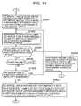
- the second MP 1141B-1 (and 1141B-2) issues a job group to copy the assigned initial dirty sub-groups A2' (and A4') to the second MP 1141B-3 (and 1141B-4) of the slave DKC module 3 (and 4) based on the management information group 200-1 (and 200-2) (see Fig. 9B ).
- the second MP 1141B-1 updates the management information group 200-1 (and 200-2) as the slave DKC module 3 (and 4) executes the job (S1902).
- the second MP 1141B-1 judges whether the dirty data elements are stored in the CM 1147-1 (and 1147-2) exceeding the first predetermined ratio based on the cache management information and management information group 200-1 (and 200-2) after update (S1903).
- the second MP 1141B-1 instructs another second MP 1141B-3 (and 1141B-4) to clear the job group, clears the division of the dirty data element group, and releases the management information group 200-1 (and 200-2) (S1904). Then the processing returns to S1100 in Fig. 11 .
- the second MP 1141B-1 judges whether copying of the initial dirty sub-group A2' (and A4') has completed in the slave DKC module 3 (and 4) (S1906).
- the second MP 1141B-1 updates the backup necessity of the dirty data elements constituting each initial dirty sub-group A2' (and A4') existing in the CM 1147-1 (and 1147-2) in the management information group 200-1 (and 200-2) from the information to indicate that backup is necessary to the information to indicate that backup is unnecessary.
- the initial dirty sub-group A2' (and A4') of which copying has completed is not erased, but remains in the CM 1147-1 (and 1147-2).
- the second MP 1141B-1 (and 1141B-2) issues the job to copy the difference dirty sub-group stored in the CM 1147-1 (and 1147-2) since forming the initial dirty sub-group A2' (and A4') or since the previous S2101, to the current time point t, to the slave DKC module 3 (and 4), while updating the management information group 200-1 (and 200-2) when a job is executed in each slave DKC module 3 (and 4), and updates the management information group that the difference dirty data element of which copy has completed becomes "backup unnecessary" (see Fig. 10A ).
- the second MP 1141B-1 judges whether the consumption ratio of the CM 1147-1 is 1/4 or more (S2102). If the consumption ratio of the CM 1147-1 (and 1147-2) has dropped to less than 1/4 (NO in S2102), the second MP 1141B-1 (and 1141B-2) updates the backup necessity corresponding to the dirty data element managed in the management information group 200-1 (and 200-2) as "backup unnecessary" to information to indicate that backup is necessary (S2104). Then the second MP 1141B-1 (and 1141B-2) instructs the second MP 1141B-3 (and 1141B-4) to clear the job group, and clears the division of the dirty data element group, and releases the management information group 200-1 (and 200-2) (s2105). Then the processing returns to S1100 in Fig. 11 .
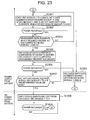
- the second MP 1141B-1 (and 1141B-2) returns to S2101, and if a power failure occurs (YES in S2103), the processing advances to S2301 in Fig. 23 (processing after S2301 will be described later).
- the occurrence of a power failure when S1905 is YES in Fig. 19 means that a failure occurred before the backup necessity of the copied dirty data element is updated to "backup unnecessary" (before S1907) in the management information group 200-1 (and 200-2).
- the second MP 1141B-1 (and 1141B-2) refers to the management information group 200-1 (and 200-2), and specifies a cache area where dirty data elements which require backup are stored, and saves the dirty data elements existing in the specified cache area to the SSD 1151-1 (and 1151-2) (S2001).
- the second MP 1141B-1 judges whether the discharge voltage (DC voltage) from the battery 118 in the power supply module 115 corresponding to the master DKC module 1 (and 2) is a predetermined value or less. If power recovers before the discharge voltage becomes a predetermined value or less (NO in S2006 and YES in S2004), the second MP 1141B-1 (and 1141B-2) can release the saved dirty data elements from the SSD 1151-1 (and 1151-2) since the saved dirty data elements remain in the CM 1147-1 (and 1147-2) because of the power supply from the battery 118 (S2005).
- the second MP 1141B-1 decides to stage the management information group 200-1 (and 200-2) from the SSD 1151-1 (and 1151-2) to the CM 1147-1 (and 1147-2) (S2201).
- the second MP 1141B-1 (and 1141B-2) also decides to stage the dirty data elements from the SSD 1151-1 (and 1151-2) to the CM 1147-1 (and 1147-2) (S2202).
- the second MP 1141B-1 (and 1141B-2) reads the data elements constituting the management information group 200-1 (and 200-2) from the SSD 1151-1 (and 1151-2) until reading the management information group 200-1 (and 200-2) to the CM 1147-1 (and 1147-2) completes (NO in S2203, and S2204).
- the second MP 1141B-1 repeats reading of the dirty data elements from the SSD 1151-1 (and 1151-2) and writing the dirty data elements to the CM 1147-1 (and 1147-2) until staging of all the saved dirty data elements to the CM 1147-1 (and 1147-2) completes (NO in S2205, and S2206).
- staging of all the dirty data elements completes (YES in S2205)
- the processing ends.
- the respective second MP 1141B-1 to 1141B-4 refers to the management information 200-1 (and 200-2) or cache management information) in each DKC module 1 to 4, and specifies a cache area where the dirty data elements which require backup are stored, and saves the dirty data elements existing in the specified cache area to the SSD 1151-1 to 1151-4 respectively (S2301).
- the dirty data elements are continuously saved until saving of the dirty data elements completes in each DKC module 1 to 4 (NO in S2304). If saving of all the dirty data elements is completed (YES in S2304), the second MP 1141B-3 (and 1141B-4) in the slave DKC module 3 (and 4) reports the completion of saving all the dirty data elements to the second MP 1141B-1 (and 1141B-2) in the master DKC module 1 (and 2). Responding to the completion report, the second MP 1141B-1 (and 1141B-2) updates the second management information 200-1 (and 200-2) (e.g.
- the second MP 1141B-1 to 1141B-4 judges whether the discharge voltage (DC voltage) from the battery 118 in the power supply module 115 corresponding to each DKC module 1 to 4 is a predetermined value or less. If power returns before the discharge voltage becomes a predetermined value or less (NO in S2307 and YES in S2306), the saved dirty data elements remain in the CM 1147-1 to 1147-4 because of the power supply from the battery 118, so the second MP 1141B-1 to 1141B-4 may release the saved dirty data elements from the SSD 1151-1 to 1151-4 (S2303).
- the second MP 1141B-1 decides to stage the management information group 200-1 (and 200-2) from the SSD 1151-1 (and 1151-2) to the CM 1147-1 (and 1147-2) (S2401).
- the second MP 1141B-1 to 1141B-4 also decide to return the duty data elements from the SSD 1151-1 to 1151-4 to the CM 1147-1 to 1147-4 (S2402).
- the second MP 1141B-3 decides to transfer the staged dirty data elements from the CM 1147-3 (and 1147-4) to the CM 1147-1 (and 1147-2) (S2403).
- the second MP 1141B-1 (and 1141B-2) decides, on the basis of the management information group 200-1 (and 200-2), to perform integration and restoration processing for the dirty data elements transferred from the slave DKC module 3 (and 4) (S2405).
- the second MP 1141B-1 to 1141B-4 repeat reading of the dirty data elements from the SSD 1151-1 to 1151-4, and writing these dirty data elements to the CM 1147-1 to 1147-4 (NO in S2406 and S2407).
- S2408 is performed.
- the dirty data elements read from the SSD 1151-1 to 1151-4, are staged in the saving source cache areas specified by the dirty data elements respectively (dotted line R1' to R4' in Fig. 10B ).
- the second MP 1141B-3 repeats transfer of the dirty data elements from the CM 1147-3 (and 1147-4) (NO in S2408 and S2409).
- S2410 is performed.
- the second MP 1141B-1 repeats the integration and restoration processing of the dirty data elements (NO in S2410, and S2411).
- the second MP 1141B-1 releases the management information group 200-1 (and 200-2) (S2412).
- the storage system 100 becomes ready status (status where receiving of I/O commands can be started) (S2413).
- the dirty data element group is divided into dirty sub-groups, which are copied to CM 1147 of other DKC modules 113 according to the above mentioned embodiments. Therefore the time required for backup, which is performed when power is supplied from the battery 118 (time for saving the dirty data elements in the CM 1147 to the SSD 1151), can be decreased. Therefore the power capacity required for backup can be decreased, and the size of the battery 118 can be decreased.
- the dirty data element group in the CM 1147-1 is divided into four dirty sub-groups, 5 MB each, and three of them are copied to CM 1147-2 to 1147-4.
- the 5 MB of dirty sub-groups stored in the CM 1147-1 to 1147-4 are saved to the SSD 1151-1 to 1151-4. Therefore the data amount to be saved from the CM 1147-1 to the SSD 1151-1 decreases from 20 MB to 5 MB, in other words, about 1/4 (the size of the management information group 200 is not considered here).
- each DKC module 1 to 4 stages the dirty data elements from the respective SSD 1151-1 to 1151-4 to the respective CM 1147-1 to 1147-4. Also the dirty data elements are transferred from the slave DKC modules 2 to 4 to the master (copy source) DKC module 1.
- the management information group 200 which was generated when the dirty data elements were copied to the other DKC modules, have been stored, and the DKC module 1 stages this management information group 200 to the CM 1147-1 with priority.
- the DKC module 1 starts integrating the dirty data elements transferred from the slave DKC modules 2 to 4, and the DKC module 1 performs restoration processing of the dirty data elements based on the management information group.
- the storage system 100 can enter the status where I/O commands can be accepted from the host computer 1100 (ready status).
- the staging time from the SSD 1151-1 to the CM 1147-1 in the DKC module 1 is about 1/4, as shown in Fig. 5B , compared with the case of saving the dirty data element group to one SSD 1151-1 (case of Fig. 5A ). Therefore the time from the return of power to system ready status (time when the storage system 100 becomes ready status) can be decreased to about 1/4.
- the transfer of the dirty data elements from the slave DKC module to the master DKC module is performed in parallel with the staging of the dirty data elements from the SSD 1151 to the CM 1147 in the slave DKC module or master DKC module, and the transfer speed of data between DKC modules, which is extremely fast compared with the data transfer speed from the SSD 1151-1 to the CM 1147-1, can be ignored.
- a controller of a general storage system is divided into a plurality of DKC modules, as shown in the examples in Fig. 1A and Fig. 2 .
- This is beneficial to a user of the storage system 100 as it decreases the installation cost of the storage system 100 and allows use of hardware resource effectively.
- the scale of the storage system may become much bigger than the scale the user expected when planning installation. In this case, the user must pay extra cost for the unnecessary hardware resources at installation.
- DKC modules can be added according to the necessity of the user (e.g. expansion of operation scale), so the user can decrease the installation cost and utilize the hardware resources effectively.
- a storage system has a structure where a controller and power supply thereof are redundant, but in the present embodiment, the controller is further divided into a plurality of DKC modules, so the influence range when a failure occurs is limited. In other words, influence can be decreased.
- the data can be written to or read from a target LDEV, or an LDEV of another DKC module. Therefore even if all the LDEVs of a certain DKC module are closed, the write data can be temporarily stored to an LDEV of another DKC module. Or even if all the MP-PKs 1137 of a certain DKC module are closed, MP 1141A or 1141B in the MP-PK 1137 in another DKC module can take over and execute the job.
- the second MP 1141B performs such processing as copying dirty data elements among the DKC modules 113, backing up of dirty data elements from the CM 1147 to the SSD 1151, and staging of the dirty data elements from the SSD 1151 to the CM 1147, but at least one of the processings may be performed by the first MP 1141A alone, or in cooperation with the second MP 1141B.
- the relationship of the above mentioned first predetermined ratio and the second predetermined ratio can be a range where the sum of (the first predetermined ratio ⁇ 1/k) and the second predetermined ratio does not exceed the first predetermined ratio.
- the dirty data volume in the CM in the master DKC module is the capacity of the CM (D max ) ⁇ first predetermined ratio
- the dirty data volume of the DKC module in the slave is Do (current dirty data volume) + D max ⁇ first predetermined ratio ⁇ 1/k, and this result must not exceed D max ⁇ first predetermined ratio, so the expression (Do + D max ⁇ first predetermined ratio ⁇ 1/k) ⁇ D max ⁇ first predetermined ratio is established, and the second predetermined ratio can be less than D 0 /D max .
Landscapes
- Engineering & Computer Science (AREA)
- Theoretical Computer Science (AREA)
- Physics & Mathematics (AREA)
- General Engineering & Computer Science (AREA)
- General Physics & Mathematics (AREA)
- Quality & Reliability (AREA)
- Memory System Of A Hierarchy Structure (AREA)
- Techniques For Improving Reliability Of Storages (AREA)
Applications Claiming Priority (1)
| Application Number | Priority Date | Filing Date | Title |
|---|---|---|---|
| JP2007216019A JP4977554B2 (ja) | 2007-08-22 | 2007-08-22 | キャッシュメモリ上のデータをバックアップする機能を備えたストレージシステム |
Publications (3)
| Publication Number | Publication Date |
|---|---|
| EP2040168A2 true EP2040168A2 (fr) | 2009-03-25 |
| EP2040168A3 EP2040168A3 (fr) | 2009-08-05 |
| EP2040168B1 EP2040168B1 (fr) | 2010-06-09 |
Family
ID=40289410
Family Applications (1)
| Application Number | Title | Priority Date | Filing Date |
|---|---|---|---|
| EP08251452A Not-in-force EP2040168B1 (fr) | 2007-08-22 | 2008-04-17 | Système de stockage doté d'une fonction de sauvegarde de données dans une mémoire cache |
Country Status (5)
| Country | Link |
|---|---|
| US (1) | US8261032B2 (fr) |
| EP (1) | EP2040168B1 (fr) |
| JP (1) | JP4977554B2 (fr) |
| CN (1) | CN101373417B (fr) |
| DE (1) | DE602008001470D1 (fr) |
Cited By (2)
| Publication number | Priority date | Publication date | Assignee | Title |
|---|---|---|---|---|
| WO2011070611A1 (fr) * | 2009-12-08 | 2011-06-16 | Hitachi, Ltd. | Système de stockage et appareil de commande de stockage pourvus de groupe de mémoire cache comprenant des mémoires volatile et non volatile |
| CN114169017A (zh) * | 2020-09-11 | 2022-03-11 | Oppo广东移动通信有限公司 | 缓存数据块下电方法、装置及集成电路芯片 |
Families Citing this family (21)
| Publication number | Priority date | Publication date | Assignee | Title |
|---|---|---|---|---|
| US20090282194A1 (en) * | 2008-05-07 | 2009-11-12 | Masashi Nagashima | Removable storage accelerator device |
| JP4952679B2 (ja) * | 2008-07-31 | 2012-06-13 | 富士通株式会社 | ストレージ管理方法、ストレージ制御装置及びストレージシステム |
| US8826351B2 (en) * | 2008-09-11 | 2014-09-02 | At&T Intellectual Property I, Lp | System and method for managing storage capacity on a digital video recorder |
| US8499120B2 (en) * | 2008-10-17 | 2013-07-30 | Seagate Technology Llc | User selectable caching management |
| US20100262773A1 (en) * | 2009-04-08 | 2010-10-14 | Google Inc. | Data striping in a flash memory data storage device |
| US8595572B2 (en) | 2009-04-08 | 2013-11-26 | Google Inc. | Data storage device with metadata command |
| US8255365B2 (en) * | 2009-06-08 | 2012-08-28 | Symantec Corporation | Source classification for performing deduplication in a backup operation |
| JP2011070365A (ja) | 2009-09-25 | 2011-04-07 | Toshiba Corp | メモリシステム |
| US8806134B2 (en) * | 2010-04-16 | 2014-08-12 | Pmc-Sierra Us, Inc. | Mirrored cache protection |
| CN102063271B (zh) * | 2010-12-17 | 2014-08-13 | 曙光信息产业(北京)有限公司 | 一种磁盘外置Cache基于状态机的写回方法 |
| WO2013186807A1 (fr) | 2012-06-11 | 2013-12-19 | Hitachi, Ltd. | Sous-système de disque et procédé de restauration de données correspondant |
| WO2014192113A1 (fr) | 2013-05-30 | 2014-12-04 | 株式会社日立製作所 | Système de stockage et procédé de sauvegarde de données |
| US9304937B2 (en) * | 2013-10-23 | 2016-04-05 | Netapp Inc. | Atomic write operations for storage devices |
| TWI718317B (zh) * | 2016-11-04 | 2021-02-11 | 南韓商三星電子股份有限公司 | 資料儲存裝置及資料處理系統 |
| US10146688B2 (en) * | 2016-12-29 | 2018-12-04 | Intel Corporation | Safe write-back cache replicating only dirty data |
| US10671494B1 (en) * | 2017-11-01 | 2020-06-02 | Pure Storage, Inc. | Consistent selection of replicated datasets during storage system recovery |
| KR102736062B1 (ko) * | 2018-08-14 | 2024-12-02 | 에스케이하이닉스 주식회사 | 입력데이터를 분산저장하기 위한 메모리 시스템 및 데이터 처리 시스템 |
| US12008413B2 (en) | 2021-07-29 | 2024-06-11 | International Business Machines Corporation | Vector processing employing buffer summary groups |
| US12554562B2 (en) | 2021-07-29 | 2026-02-17 | International Business Machines Corporation | Intersystem processing employing buffer summary groups |
| CN114006060B (zh) * | 2021-10-29 | 2023-07-07 | 蜂巢能源科技(无锡)有限公司 | 一种储能电池管理系统 |
| US20240004761A1 (en) * | 2022-06-30 | 2024-01-04 | Commvault Systems, Inc. | Low impact migration of large data to cloud and virtualized environments |
Citations (2)
| Publication number | Priority date | Publication date | Assignee | Title |
|---|---|---|---|---|
| JP2002099390A (ja) | 2000-09-22 | 2002-04-05 | Toshiba Corp | ディスク制御装置 |
| JP2007216019A (ja) | 2006-02-14 | 2007-08-30 | Gerresheimer Buende Gmbh | 前充填可能な注射器を製作する方法 |
Family Cites Families (11)
| Publication number | Priority date | Publication date | Assignee | Title |
|---|---|---|---|---|
| GB2256735B (en) | 1991-06-12 | 1995-06-21 | Intel Corp | Non-volatile disk cache |
| JPH07504527A (ja) * | 1992-03-09 | 1995-05-18 | オースペックス システムズ インコーポレイテッド | 高性能の不揮発性ram保護式の書き込みキャッシュアクセラレータシステム |
| JP3239669B2 (ja) * | 1995-02-20 | 2001-12-17 | 株式会社日立製作所 | 記憶制御装置及びその制御方法 |
| JPH09244954A (ja) * | 1996-03-11 | 1997-09-19 | Toshiba Corp | 情報記憶装置 |
| US6513097B1 (en) * | 1999-03-03 | 2003-01-28 | International Business Machines Corporation | Method and system for maintaining information about modified data in cache in a storage system for use during a system failure |
| JP2003099384A (ja) * | 2001-09-20 | 2003-04-04 | Nec Corp | 負荷分散システム、負荷分散システムのホストコンピュータ、及び負荷分散プログラム |
| US7085886B2 (en) * | 2003-05-28 | 2006-08-01 | International Buisness Machines Corporation | Autonomic power loss recovery for a multi-cluster storage sub-system |
| JP4147198B2 (ja) * | 2004-03-23 | 2008-09-10 | 株式会社日立製作所 | ストレージシステム |
| JP2005004791A (ja) * | 2004-08-23 | 2005-01-06 | Hitachi Ltd | ディスク制御装置 |
| US20060212644A1 (en) | 2005-03-21 | 2006-09-21 | Acton John D | Non-volatile backup for data cache |
| JP4662550B2 (ja) * | 2005-10-20 | 2011-03-30 | 株式会社日立製作所 | ストレージシステム |
-
2007
- 2007-08-22 JP JP2007216019A patent/JP4977554B2/ja not_active Expired - Fee Related
-
2008
- 2008-02-05 US US12/068,321 patent/US8261032B2/en not_active Expired - Fee Related
- 2008-04-17 DE DE602008001470T patent/DE602008001470D1/de active Active
- 2008-04-17 EP EP08251452A patent/EP2040168B1/fr not_active Not-in-force
- 2008-06-03 CN CN2008100986299A patent/CN101373417B/zh not_active Expired - Fee Related
Patent Citations (2)
| Publication number | Priority date | Publication date | Assignee | Title |
|---|---|---|---|---|
| JP2002099390A (ja) | 2000-09-22 | 2002-04-05 | Toshiba Corp | ディスク制御装置 |
| JP2007216019A (ja) | 2006-02-14 | 2007-08-30 | Gerresheimer Buende Gmbh | 前充填可能な注射器を製作する方法 |
Cited By (3)
| Publication number | Priority date | Publication date | Assignee | Title |
|---|---|---|---|---|
| WO2011070611A1 (fr) * | 2009-12-08 | 2011-06-16 | Hitachi, Ltd. | Système de stockage et appareil de commande de stockage pourvus de groupe de mémoire cache comprenant des mémoires volatile et non volatile |
| US8327069B2 (en) | 2009-12-08 | 2012-12-04 | Hitachi, Ltd. | Storage system and storage control apparatus provided with cache memory group including volatile memory and nonvolatile memory |
| CN114169017A (zh) * | 2020-09-11 | 2022-03-11 | Oppo广东移动通信有限公司 | 缓存数据块下电方法、装置及集成电路芯片 |
Also Published As
| Publication number | Publication date |
|---|---|
| US20090055590A1 (en) | 2009-02-26 |
| JP2009048544A (ja) | 2009-03-05 |
| EP2040168A3 (fr) | 2009-08-05 |
| EP2040168B1 (fr) | 2010-06-09 |
| CN101373417A (zh) | 2009-02-25 |
| CN101373417B (zh) | 2010-12-29 |
| US8261032B2 (en) | 2012-09-04 |
| JP4977554B2 (ja) | 2012-07-18 |
| DE602008001470D1 (de) | 2010-07-22 |
Similar Documents
| Publication | Publication Date | Title |
|---|---|---|
| EP2040168B1 (fr) | Système de stockage doté d'une fonction de sauvegarde de données dans une mémoire cache | |
| JP5916958B2 (ja) | 計算機システム及び計算機システム制御方法 | |
| WO2010064280A1 (fr) | Système de stockage à mémoire volatile et mémoire non volatile | |
| JP7247290B2 (ja) | ストレージシステム | |
| WO2013057764A1 (fr) | Système de mémoire | |
| JP6136460B2 (ja) | 情報処理装置、情報処理装置の制御プログラムおよび情報処理装置の制御方法 | |
| EP2557494B1 (fr) | Appareil de stockage et procédé de copie de données | |
| US20060080362A1 (en) | Data Synchronization Over a Computer Network | |
| WO2011104741A1 (fr) | Système de gestion pour système de stockage et procédé de gestion de système de stockage | |
| JP2010123066A (ja) | オンラインボリュームと性能/障害独立かつ容量効率の高いスナップショットを実現するストレージシステム及び方法 | |
| JP6822274B2 (ja) | 情報処理システム、方法、及びプログラム | |
| JP7208000B2 (ja) | 情報処理装置及び情報処理装置の制御方法 | |
| JP2013114624A (ja) | ストレージシステム及びプール容量縮小の制御方法 | |
| CN103761053A (zh) | 一种数据处理方法和装置 | |
| JP2005108098A (ja) | データi/o装置及びデータi/o装置の制御方法 | |
| WO2010097832A1 (fr) | Système de stockage comprenant un groupe raid | |
| JP2021026512A (ja) | ストレージシステムおよびストレージ制御方法 | |
| JPWO2015097751A1 (ja) | 不揮発性キャッシュメモリにデータをバックアップするストレージシステム | |
| CN102347866A (zh) | 网络管理中的数据配置系统及配置方法 | |
| WO2013118189A1 (fr) | Procédé de remplacement de dispositif de mémorisation, et sous-système de mémorisation adoptant un procédé de remplacement de dispositif de mémorisation | |
| WO2014087453A1 (fr) | Dispositif de stockage et procédé de commande du dispositif de stockage | |
| US20120102242A1 (en) | Controlling data destaging within a multi-tiered storage system | |
| JP5712535B2 (ja) | ストレージ装置、制御部およびストレージ装置制御方法 | |
| WO2013136371A1 (fr) | Système de stockage et procédé de gestion de données | |
| US20130086345A1 (en) | Storage apparatus, control apparatus, and storage apparatus control method |
Legal Events
| Date | Code | Title | Description |
|---|---|---|---|
| PUAI | Public reference made under article 153(3) epc to a published international application that has entered the european phase |
Free format text: ORIGINAL CODE: 0009012 |
|
| 17P | Request for examination filed |
Effective date: 20080506 |
|
| AK | Designated contracting states |
Kind code of ref document: A2 Designated state(s): AT BE BG CH CY CZ DE DK EE ES FI FR GB GR HR HU IE IS IT LI LT LU LV MC MT NL NO PL PT RO SE SI SK TR |
|
| AX | Request for extension of the european patent |
Extension state: AL BA MK RS |
|
| PUAL | Search report despatched |
Free format text: ORIGINAL CODE: 0009013 |
|
| AK | Designated contracting states |
Kind code of ref document: A3 Designated state(s): AT BE BG CH CY CZ DE DK EE ES FI FR GB GR HR HU IE IS IT LI LT LU LV MC MT NL NO PL PT RO SE SI SK TR |
|
| AX | Request for extension of the european patent |
Extension state: AL BA MK RS |
|
| GRAP | Despatch of communication of intention to grant a patent |
Free format text: ORIGINAL CODE: EPIDOSNIGR1 |
|
| AKX | Designation fees paid |
Designated state(s): DE FR GB IE |
|
| GRAS | Grant fee paid |
Free format text: ORIGINAL CODE: EPIDOSNIGR3 |
|
| GRAA | (expected) grant |
Free format text: ORIGINAL CODE: 0009210 |
|
| AK | Designated contracting states |
Kind code of ref document: B1 Designated state(s): DE FR GB IE |
|
| REG | Reference to a national code |
Ref country code: IE Ref legal event code: FG4D |
|
| REF | Corresponds to: |
Ref document number: 602008001470 Country of ref document: DE Date of ref document: 20100722 Kind code of ref document: P |
|
| PLBE | No opposition filed within time limit |
Free format text: ORIGINAL CODE: 0009261 |
|
| STAA | Information on the status of an ep patent application or granted ep patent |
Free format text: STATUS: NO OPPOSITION FILED WITHIN TIME LIMIT |
|
| REG | Reference to a national code |
Ref country code: DE Ref legal event code: R097 Ref document number: 602008001470 Country of ref document: DE Effective date: 20110309 |
|
| REG | Reference to a national code |
Ref country code: FR Ref legal event code: ST Effective date: 20111230 |
|
| PG25 | Lapsed in a contracting state [announced via postgrant information from national office to epo] |
Ref country code: FR Free format text: LAPSE BECAUSE OF NON-PAYMENT OF DUE FEES Effective date: 20110502 |
|
| REG | Reference to a national code |
Ref country code: IE Ref legal event code: MM4A |
|
| PG25 | Lapsed in a contracting state [announced via postgrant information from national office to epo] |
Ref country code: IE Free format text: LAPSE BECAUSE OF NON-PAYMENT OF DUE FEES Effective date: 20110417 |
|
| PGFP | Annual fee paid to national office [announced via postgrant information from national office to epo] |
Ref country code: GB Payment date: 20220303 Year of fee payment: 15 |
|
| PGFP | Annual fee paid to national office [announced via postgrant information from national office to epo] |
Ref country code: DE Payment date: 20220302 Year of fee payment: 15 |
|
| REG | Reference to a national code |
Ref country code: DE Ref legal event code: R119 Ref document number: 602008001470 Country of ref document: DE |
|
| GBPC | Gb: european patent ceased through non-payment of renewal fee |
Effective date: 20230417 |
|
| PG25 | Lapsed in a contracting state [announced via postgrant information from national office to epo] |
Ref country code: GB Free format text: LAPSE BECAUSE OF NON-PAYMENT OF DUE FEES Effective date: 20230417 |
|
| PG25 | Lapsed in a contracting state [announced via postgrant information from national office to epo] |
Ref country code: GB Free format text: LAPSE BECAUSE OF NON-PAYMENT OF DUE FEES Effective date: 20230417 Ref country code: DE Free format text: LAPSE BECAUSE OF NON-PAYMENT OF DUE FEES Effective date: 20231103 |