EP2040302A1 - Dispositif à semi-conducteur - Google Patents
Dispositif à semi-conducteur Download PDFInfo
- Publication number
- EP2040302A1 EP2040302A1 EP07767367A EP07767367A EP2040302A1 EP 2040302 A1 EP2040302 A1 EP 2040302A1 EP 07767367 A EP07767367 A EP 07767367A EP 07767367 A EP07767367 A EP 07767367A EP 2040302 A1 EP2040302 A1 EP 2040302A1
- Authority
- EP
- European Patent Office
- Prior art keywords
- semiconductor
- thickness
- semiconductor device
- region
- layer
- Prior art date
- Legal status (The legal status is an assumption and is not a legal conclusion. Google has not performed a legal analysis and makes no representation as to the accuracy of the status listed.)
- Withdrawn
Links
Images




Classifications
-
- H—ELECTRICITY
- H10—SEMICONDUCTOR DEVICES; ELECTRIC SOLID-STATE DEVICES NOT OTHERWISE PROVIDED FOR
- H10D—INORGANIC ELECTRIC SEMICONDUCTOR DEVICES
- H10D30/00—Field-effect transistors [FET]
- H10D30/60—Insulated-gate field-effect transistors [IGFET]
- H10D30/67—Thin-film transistors [TFT]
- H10D30/6758—Thin-film transistors [TFT] characterised by the insulating substrates
-
- H—ELECTRICITY
- H10—SEMICONDUCTOR DEVICES; ELECTRIC SOLID-STATE DEVICES NOT OTHERWISE PROVIDED FOR
- H10D—INORGANIC ELECTRIC SEMICONDUCTOR DEVICES
- H10D30/00—Field-effect transistors [FET]
- H10D30/60—Insulated-gate field-effect transistors [IGFET]
- H10D30/67—Thin-film transistors [TFT]
- H10D30/6729—Thin-film transistors [TFT] characterised by the electrodes
- H10D30/673—Thin-film transistors [TFT] characterised by the electrodes characterised by the shapes, relative sizes or dispositions of the gate electrodes
- H10D30/6733—Multi-gate TFTs
- H10D30/6734—Multi-gate TFTs having gate electrodes arranged on both top and bottom sides of the channel, e.g. dual-gate TFTs
-
- H—ELECTRICITY
- H10—SEMICONDUCTOR DEVICES; ELECTRIC SOLID-STATE DEVICES NOT OTHERWISE PROVIDED FOR
- H10D—INORGANIC ELECTRIC SEMICONDUCTOR DEVICES
- H10D30/00—Field-effect transistors [FET]
- H10D30/60—Insulated-gate field-effect transistors [IGFET]
- H10D30/67—Thin-film transistors [TFT]
- H10D30/674—Thin-film transistors [TFT] characterised by the active materials
- H10D30/6741—Group IV materials, e.g. germanium or silicon carbide
- H10D30/6743—Silicon
- H10D30/6744—Monocrystalline silicon
-
- H—ELECTRICITY
- H10—SEMICONDUCTOR DEVICES; ELECTRIC SOLID-STATE DEVICES NOT OTHERWISE PROVIDED FOR
- H10D—INORGANIC ELECTRIC SEMICONDUCTOR DEVICES
- H10D62/00—Semiconductor bodies, or regions thereof, of devices having potential barriers
- H10D62/10—Shapes, relative sizes or dispositions of the regions of the semiconductor bodies; Shapes of the semiconductor bodies
Definitions
- This invention relates to a semiconductor device, such as an IC and an LSI, and, in particular, to an accumulation-mode MOS transistor.
- Patent Document 1 proposes the semiconductor device provided with a circuit having at least one pair of transistors of different conductivity types in which at least one of the transistors includes at least a semiconductor layer formed on an SOI base substrate, a gate insulating layer covering at least a part of a surface thereof, and a gate electrode formed on the gate insulating film, and is formed as a normally-off accumulation mode transistor.
- a material of the gate electrode and an impurity concentration of the semiconductor layer are selected in such a manner that a thickness of a depletion layer formed in the semiconductor layer by a difference in work function (work function difference) between the gate electrode and the semiconductor layer is greater than a film thickness of the semiconductor layer.
- Patent Document 1 discloses that, for the purpose of equalizing current driving capabilities of a p-channel transistor and an n-channel transistor constituting CMOS transistors, the current driving capability of the p-channel transistor can be enhanced by using a (110) plane of silicon. According to this structure, switching speeds of the n-channel transistor and the p-channel transistor can substantially be equalized and areas occupied by electrodes formed on channel regions can substantially be equalized.
- Patent Document 1 Japanese Patent Application No. 2005-349857
- Patent Document 1 discloses that the accumulation-mode MOS transistor can be normally off by a work function difference between the gate electrode and the SOI layer.
- the gate electrode is formed with polycrystalline silicon containing boron of not less than 10 20 cm -3 and the SOI layer is formed by an n-type silicon layer having an impurity concentration of 10 17 cm -3
- a work function difference of approximately 0.9eV is produced, because P+polycrystalline silicon having the mentioned impurity concentration has a work function of approximately 5.15eV and the n-type silicon having the mentioned impurity concentration has a work function of approximately 4.25eV.
- the depletion layer has a thickness of about 90nm. Therefore, if the SOI layer has a thickness of 45nm, the SOI layer is fully depleted and a normally-off transistor can be obtained.
- the material of the gate electrode is limited.
- Ta is intended to be used for the gate electrode
- the use is difficult. This is because its work function is 4.6eV and has only a very slight difference from that of the SOI layer.
- it is required to make the impurity concenration of the SOI layer high in order to increase the current driving capability of the transistor, because a bulk current flows through the entire SOI layer in addition to an electric current of an accumulation layer when the transistor is turned on. As the impurity concentration of the SOI layer is higher, the bulk current of the entire SOI layer becomes higher and a 1/f noise decreases.
- the SOI layer desirably has a high impurity concentration.
- the impurity concentration of the SOI layer is one digit greater, the thickness of the depletion layer is reduced to 1/4 to 1/7. Therefore, it is required to reduce the film thickness of the SOI layer.
- the bulk current of the entire SOI layer is reduced. Consequently, the material of the gate electrode must have a greater difference in work function from the SOI layer. As a result, a threshold voltage of the transistor is made high and driving the transistor at a low power supply voltage becomes difficult.
- a semiconductor device formed by using a base substrate having at least a first semiconductor region, a buried insulating layer formed thereon, and a second semiconductor region formed on the buried insulating layer, at least a part of the second semiconductor region serving as a channel region, a gate insulating film formed on the channel region, and a gate electrode formed thereon, wherein a thickness of a depletion layer in the channel region is controlled by a thickness of the buried insulating layer and an impurity concentration of the second semiconductor region.
- a threshold value depends on the thickness of the buried insulating layer and the impurity concentration of the first semiconductor region.
- the semiconductor device wherein the semiconductor device has a source region and a drain region electrically connected to the channel region, the gate electrode being constructed by at least partially using a material having a work function different from that of the channel region, the thickness of the depletion layer in the channel region being determined by adjusting a work function difference between the gate electrode and the channel region, the impurity concentration of the first semiconductor region, and the thickness of the buried insulating layer.
- the impurity concentration of the second semiconductor region is preferably 10 17 cm -3 , more preferably 2 x 10 17 m -3 .
- the semiconductor device wherein the threshold value is smaller than that determined by the work function difference between the gate electrode and the channel region.
- the semiconductor device wherein the first semiconductor region and the second semiconductor region are made of silicons having opposite conductivity types to each other.
- the semiconductor device wherein the semiconductor device is of an accumulation mode with the channel region, the source region, and the drain region having the same conductivity type.
- the semiconductor device wherein the semiconductor device is of a normally-off type.
- the semiconductor device wherein the buried insulating layer has a thickness which is not greater than 20nm and which preferably satisfies the following formula.
- T BOX and T SOI denote EOT (Effective Oxide Thickness, namely, equivalent SiO 2 thickness) of the buried insulating layer and a thickness of the second semiconductor region, respectively.
- a ninth aspect of the present invention three is provided a method of manufacturing a semiconductor device formed on a base substrate having a buried insulating layer and having a gate electrode and a threshold value, wherein the threshold value is controlled by adjusting an impurity concentration of the base substrate.
- the method of manufacturing a semiconductor device wherein the impurity concentration of the base substrate is adjusted by ion implantation
- a semiconductor device comprising a semiconductor layer having two principal faces, a gate electrode formed on one face of the semiconductor layer with a gate insulating film inserted therebetween, and a conductive layer formed on the other face of the semiconductor layer with a buried insulating layer inserted therebetween, wherein at least a part of the semiconductor layer is used as a channel region and the buried insulating layer has a thickness not greater than 20nm, a thickness of a depletion layer in the channel region being made greater than that of the semiconductor layer by a thickness of the buried insulating layer, a work function difference between a material of the gate electrode and the semiconductor layer, and a work function difference between the conductive layer and the semiconductor layer.
- a new semiconductor device in which a thickness of a depletion layer in a channel region is reduced by reducing a film thickness of a buried insulating layer and controlled by an impurity concentration of a semiconductor region on a base substrate side.
- normally-off can be achieved without increasing a threshold value by adjusting an impurity concentration of a base substrate either without performing control by a work function difference between a gate electrode and a channel region or in combination with such control.
- the present invention is advantageous in that a semiconductor device having a low threshold voltage and reduced in size can be obtained. That is, in the present invention, a semiconductor device operable at a high speed and a low power supply voltage can be constructed.
- FIG. 1 an accumulation-mode MOS transistor and an inversion-mode MOS transistor are shown, to which the present invention is applicable.
- Fig. 1 (a) and (b) show n-channel and p-channel accumulation-mode MOS transistors (an NMOS transistor and a PMOS transistor), respectively
- Fig. 1 (c) and (d) show n-channel and p-channel inversion-mode MOS transistors, respectively.
- a buried insulating layer (BOX) is formed on a surface region of a p-type silicon base substrate.
- BOX buried insulating layer
- an n-type SOI (Silicon On Insulator) layer is formed on the buried insulating layer (BOX).
- the n-type SOI layer forms source, drain, and channel regions.
- each of the source and the drain regions has an impurity concentration higher than that of the channel region.
- the source and the drain regions are connected to a source electrode S and a drain electrode D, respectively.
- a gate insulating film is formed on the channel region.
- a gate electrode of p-type polycrystalline silicon is formed on the gate insulating film.
- a buried insulating layer (BOX) is formed on an n-type silicon base substrate.
- a p-type SOI layer constituting source, drain, and channel regions is formed.
- Each of the source and the drain regions has an impurity concentration higher than that of the channel region.
- a gate electrode of n-type polycrystalline silicon is formed with a gate insulating film intermediate therebetween.
- Fig. 1 (c) and (d) show similar structures as illustrated in the figure.
- each of the NMOS transistor and the PMOS transistor in Fig. 1 (a) and (b) when a gate voltage Vg is zero, a depletion layer spreads throughout the SOI layer. When the gate voltage Vg is applied, the depletion layer retreats to an upper surface of the channel region. Further, when the gate voltage Vg becomes higher, each transistor performs an operation such that an accumulation current flows in addition to a bulk current. Each of the NMOS transistor and the PMOS transistor in Fig. 1 (c) and (d) is off when the gate voltage Vg is zero. When the gate voltage Vg is applied, an inversion layer is formed on an upper surface of a channel region and an electric current flows between source and drain regions.
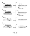
- Fig. 2 (a) through (d) show an operating principle of the accumulation-mode NMOS transistor mentioned above.
- the gate voltage Vg when the gate voltage Vg is zero, the depletion layer spreads throughout the SOI layer.
- Fig. 2 (b) when the gate voltage Vg is applied, the depletion layer retreats to the upper surface of the channel region and a bulk current lbulk starts to flow. Further, when the gate voltage Vg increases, an accumulation current lacc also starts to flow, as shown in Fig. 2 (c) and (d) .
- Fig. 3 (a) and (b) Let an SOI structure be used and the depletion layer generated by the work function difference between the gate electrode and the SOI layer have a thickness greater than that of the SOI layer. Then, a normally-off type MOS transistor having an accumulation structure as shown in Fig. 3 (a) can be achieved.
- p+polysilicon having a work function of 5.2eV
- n+polysilicon having a work function of 4.1 eV
- the present inventors prepared an accumulation-mode NMOS transistor in which a silicon base substrate and an SOI layer are inverse in conductivity type from each other and a buried insulating layer (BOX) has a thickness of 100nm, like the MOS transistors shown in Fig. 1 (a) and (b) (especially, the NMOS transistor), and conducted an experiment.
- the NMOS transistor used in the experiment has a structure same as that described in Patent Document 1.
- As a silicon base substrate a P-type silicon base substrate having an impurity concentration of 1 x 10 15 cm -3 was used.
- the threshold value of the NMOS transistor having the above-mentioned structure depends only on the work function difference between the gate electrode and the SOI layer.
- the accumulation-mode NMOS transistor using the buried insulating layer (BOX) having a thickness of approximately 100nm it is not possible to change the threshold voltage determined by the work function difference, even if the impurity concentration of the silicon base substrate is changed.
- Ta having a work function of 4.6V
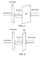
- the SOI layer has been controlled only on a gate electrode side because the buried insulating layer (BOX) is thick, as shown in Fig. 4 .
- the present inventors found out a phenomenon that an electric potential of the SOI layer can also be controlled from a base substrate side by reducing the thickness of the buried insulating layer (BOX), as shown in Fig. 5 .
- the thickness (T BOX ) of the buried insulating layer (BOX) was reduced to less than 20nm.
- the silicon base substrate as a supporting base substrate was subjected to ion implantation from its surface (a side on which the gate electrode is later constructed) to obtain an NMOS transistor in which an impurity concentration (NBase) of the silicon base substrate was changed.
- a drain voltage Vd of 1 V was applied to the transistor and changes in drain current were observed.
- a threshold value of the NMOS transistor was changed depending on the impurity concentration (NBase) of the silicon base substrate.
- the SOI layer and the base substrate are inverse in conductivity type from each other.
- the SOI layer is depleted by a work function difference between the base substrate and the SOI layer.
- a gate electrode such as a Ta gate electrode
- the threshold value can effectively be controlled by adjusting the thickness of the buried insulating layer (BOX) and/or the impurity concentration of the SOI layer.
- the threshold value can finely be adjusted by controlling the concentration of the supporting base substrate.
- a conductive material having a large difference in work function from the SOI layer may also be used for a base substrate material.
- an impurity concentration N(x) in a depth direction (x) of the base substrate is given by the following formula 1:
- N x Q 2 ⁇ ⁇ ⁇ ⁇ R p 2 ⁇ exp - ( x - R p ⁇ ) 2 2 ⁇ ⁇ R p 2
- Q, Rp, and ⁇ Rp 2 denote an implantation dose, a projected range, and a standard deviation, respectively.
- N mzx Q 2 ⁇ ⁇ ⁇ ⁇ R p 2
- N(x) must be controlled within a range of 0.2N max to 0.5N max .
- ⁇ Rp can be approximated by 0.3Rp. Therefore, a relationship of 0.36Rp ⁇ x ⁇ 0.46Rp is obtained.
- a formula of 0.56T SOI ⁇ T BOX ⁇ 0.85T SOI is derived from (0.36/0.64)T SOI ⁇ T BOX ⁇ (0.46/0.54)T SOI .
- T BOX and T SOI denote an EOT (Effective Oxide Thickness, namely, equivalent SiO 2 thickness) of the buried insulating layer and the thickness of the SOI layer, respectively.
- an effective channel length (Leff) and a channel width (W) of the transistor are 45nm and 1 ⁇ m, respectively.
- An equivalent SiO 2 thickness (EOT) of a gate insulating film is 1nm and a thickness (TSOI) of the SOI layer is 15nm.
- An impurity concentration (Nsub) of a channel region in the SOI layer is 2 x 10 17 cm -3 .
- tantalum (Ta) having a work function (WF) of 4.6V is used as a gate electrode.
- Fig. 6 shows the characteristic in case where an electric voltage of 1 V as a drain voltage Vd is applied to a drain electrode.
- a thickness (TBOX) of a buried insulating layer and an impurity concentration (NBase) of a silicon supporting base substrate are changed.
- a curve C1 shows a gate voltage - drain current characteristic when NBase is 1 x 10 18 cm -3 and TBOX is 12nm.
- a curve C2 shows a gate voltage - drain current characteristic when NBase is 1 x 10 18 cm -3 and TBOX is 15um.
- a curve C3 shows a gate voltage - drain current characteristic when NBase is 1 x 10 18 cm -3 and TBOX is 20nm.
- curves C4 and C5 show gate voltage - drain current characteristics when TBOX is 20nm and when NBase is 1 x 10 17 cm -3 and 1 x 10 16 cm -3 , respectively.
- the gate voltage - drain current characteristic is changed also by the impurity concentration (NBase) of the silicon base substrate as the supporting base substrate. As a result, even with the Ta gate electrode, normally-off can be achieved. Further, depending on the thickness (TBOX) of the buried insulating layer, the gate voltage - drain current characteristic can be controlled and a threshold voltage (by the constant current method, the threshold voltage is defined as a gate voltage when an electric current of 1 ⁇ A flows) can be controlled to 0.05 to 0.2V.
- the threshold voltage of the NMOS transistor can be changed depending on the impurity concentration (NBase) of the silicon base substrate when the thickness (TBOX) of the buried insulating layer is 20nm or less. It is understood from the curves C1 to C3 that the threshold voltage can be changed by changing the thickness (TBOX) of the buried insulating layer. By adjusting the impurity concentration of the supporting base substrate, the threshold value can finely be adjusted.
- the threshold voltages can finely be adjusted by the impurity concentration (NBase) of the silicon base substrate, as is clear from the curves C3 to C5. However, if the thickness is greater, the threshold voltage no longer depends on the impurity concentration of the silicon base substrate.
- the threshold voltage can finely be adjusted.
- a gate voltage - drain current characteristic is shown when the impurity concentration (Nsub) of the SOI layer and the thickness (TBOX) of the buried insulating layer are changed in a state where the impurity concentration (NBase) of the silicon base substrate is kept constant.
- an accumulation-mode NMOS transistor as an object has an effective channel length (Leff) of 45 nm and a channel width (W) of 1 ⁇ m.
- an equivalent SiO 2 thickness (EOT) of a gate insulating film is 1 nm and a thickness (TSOI) of the SOI layer is 15nm.
- an impurity concentration (NBase) of the silicon base substrate is 1 x 10 18 cm -3 and, as a gate electrode, tantalum (Ta) having a work function (WF) of 4.6V was used. Also in Fig. 7 , an electric voltage of 1 V as a drain voltage Vd was applied to a drain electrode.
- each of curves C6 and C7 shown in Fig. 7 is the characteristic when the buried insulating layer has a thickness (TBOX) of 12nm.
- each of curves C8 and C9 is the characteristic when the buried insulating layer has a thickness (TBOX) of 15nm.
- each of the curves C6 and C8 is the characteristic when the SOI layer has an impurity concentration (Nsub) of 5 x10 17 cm -3 .
- Each of the curves C7 and C9 is the characteristic when the SOI layer has an impurity concentration (Nsub) of 2 x 10 17 cm -3 .
- the threshold voltage can be controlled.
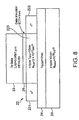
- the semiconductor device shown in the figure is an accumulation-mode NMOS transistor using an SOI layer 22 formed on a P-type silicon base substrate 20 with a buried insulating layer 24 intermediate therebetween.
- the buried insulating layer 24 having a thickness (TBOX) of 12nm and made of SiO 2 is formed.
- the P-type silicon base substrate 20 is doped with impurities by ion implantation through the buried insulating layer 24 and its surface impurity concentration (Nbase) is adjusted to 10 18 cm -3 . That is, the semiconductor device shown in the figure can be manufactured by adding a process of implanting ions through the buried insulating layer 24.
- the SOI layer 22 is an N-type layer which has a thickness (TSOI) of 15nm and a conductivity type inverse to that of the silicon base substrate 20.
- the SOI layer 22 has a source region 221, a drain region 222, and a channel region 223.
- the channel region 223 has an impurity concentration (Nsub) of 2 x 10 17 cm -3 and each of the source region 221 and the drain region 222 has an impurity concentration higher than that of the channel region 223.
- the channel region 223 has an effective length (Leff) of 45nm and a width (W) of 1 ⁇ m.
- a gate insulating film 26 having an equivalent SiO 2 thickness (EOT) of 1 nm is formed on the gate insulating film 26, a gate electrode 28 formed by a Ta material having a work function (WF) of 4.6V is provided on the gate insulating film 26.
- the gate electrode 28 has a length (L) of 0.045nm and a width (W) of 1 ⁇ m.
- the buried insulating layer 24 may also be formed by a different material, such as Si 3 N 4 , having an EOT of 12nm.
- the gate electrode 28 can be formed by using Ta having a low work function (WF). As a result, it is possible to obtain a transistor having a low threshold voltage. Therefore, the NMOS transistor shown in the figure is applicable also to a circuit having a low voltage source.
- accumulation-mode NMOS transistor has been described.
- present invention is similarly applicable also to an accumulation-mode PMOS transistor.
- the depletion layer in the channel region of the SOI layer can be controlled from an under side to thereby adjust the threshold value by controlling the thickness of the BOX layer, the impurity concentration of the base substrate, and the impurity concentration of the SOI layer.
- a base substrate bias effect depending on the impurity concentration of the base substrate can be used.
- CMOS complementary metal-oxide-semiconductor
- present invention is also applicable to an inversion-mode MOS transistor and, in a combination of the accumulation-mode MOS transistor and the inversion-mode MOS transistor, to each or both of these transistors.
Landscapes
- Thin Film Transistor (AREA)
- Metal-Oxide And Bipolar Metal-Oxide Semiconductor Integrated Circuits (AREA)
Applications Claiming Priority (2)
| Application Number | Priority Date | Filing Date | Title |
|---|---|---|---|
| JP2006176945A JP5329024B2 (ja) | 2006-06-27 | 2006-06-27 | 半導体装置 |
| PCT/JP2007/062541 WO2008001680A1 (fr) | 2006-06-27 | 2007-06-21 | Dispositif à semi-conducteur |
Publications (2)
| Publication Number | Publication Date |
|---|---|
| EP2040302A1 true EP2040302A1 (fr) | 2009-03-25 |
| EP2040302A4 EP2040302A4 (fr) | 2011-05-18 |
Family
ID=38845446
Family Applications (1)
| Application Number | Title | Priority Date | Filing Date |
|---|---|---|---|
| EP07767367A Withdrawn EP2040302A4 (fr) | 2006-06-27 | 2007-06-21 | Dispositif à semi-conducteur |
Country Status (7)
| Country | Link |
|---|---|
| US (1) | US8643106B2 (fr) |
| EP (1) | EP2040302A4 (fr) |
| JP (1) | JP5329024B2 (fr) |
| KR (1) | KR20090032081A (fr) |
| CN (1) | CN101512774B (fr) |
| TW (1) | TWI453914B (fr) |
| WO (1) | WO2008001680A1 (fr) |
Families Citing this family (12)
| Publication number | Priority date | Publication date | Assignee | Title |
|---|---|---|---|---|
| US7812397B2 (en) * | 2005-09-29 | 2010-10-12 | International Business Machines Corporation | Ultra thin channel (UTC) MOSFET structure formed on BOX regions having different depths and different thicknesses beneath the UTC and source/drain regions and method of manufacture thereof |
| US8985883B2 (en) | 2007-07-30 | 2015-03-24 | The Procter & Gamble Company | Control surfaces for applicator with moveable applicator head |
| JP5299752B2 (ja) * | 2008-04-28 | 2013-09-25 | 国立大学法人東北大学 | 半導体装置 |
| US8957462B2 (en) | 2010-12-09 | 2015-02-17 | Semiconductor Energy Laboratory Co., Ltd. | Semiconductor device comprising an N-type transistor with an N-type semiconductor containing nitrogen as a gate |
| US8513773B2 (en) | 2011-02-02 | 2013-08-20 | Semiconductor Energy Laboratory Co., Ltd. | Capacitor and semiconductor device including dielectric and N-type semiconductor |
| US9001564B2 (en) | 2011-06-29 | 2015-04-07 | Semiconductor Energy Laboratory Co., Ltd. | Semiconductor device and a method for driving the same |
| CN103367141B (zh) * | 2012-04-09 | 2016-06-01 | 中芯国际集成电路制造(上海)有限公司 | 功函数测试方法 |
| JP2013012768A (ja) * | 2012-09-05 | 2013-01-17 | Tohoku Univ | 半導体装置 |
| US9698235B2 (en) | 2013-10-22 | 2017-07-04 | National Institute Of Advanced Industrial Science And Technology | Field-effect transistor |
| CN103560144B (zh) * | 2013-11-13 | 2016-02-17 | 北京大学 | 抑制隧穿晶体管泄漏电流的方法及相应的器件和制备方法 |
| US9252228B2 (en) | 2013-11-29 | 2016-02-02 | Qualcomm Incorporated | Threshold voltage adjustment in metal oxide semiconductor field effect transistor with silicon oxynitride polysilicon gate stack on fully depleted silicon-on-insulator |
| KR102841804B1 (ko) * | 2022-07-29 | 2025-08-05 | 한국항공대학교산학협력단 | 노멀리-오프 반도체 소자 및 그 제조 방법 |
Family Cites Families (20)
| Publication number | Priority date | Publication date | Assignee | Title |
|---|---|---|---|---|
| US5111260A (en) * | 1983-06-17 | 1992-05-05 | Texax Instruments Incorporated | Polysilicon FETs |
| JPS63198374A (ja) * | 1987-02-13 | 1988-08-17 | Fujitsu Ltd | 半導体装置 |
| JPH05235350A (ja) * | 1992-02-26 | 1993-09-10 | Fujitsu Ltd | 半導体装置 |
| JP3488730B2 (ja) * | 1993-11-05 | 2004-01-19 | 株式会社ルネサステクノロジ | 半導体集積回路装置 |
| US6498376B1 (en) * | 1994-06-03 | 2002-12-24 | Seiko Instruments Inc | Semiconductor device and manufacturing method thereof |
| JP3470133B2 (ja) | 1994-06-03 | 2003-11-25 | セイコーインスツルメンツ株式会社 | 半導体装置の製造方法 |
| JPH08222705A (ja) * | 1995-02-14 | 1996-08-30 | Hitachi Ltd | 相補型半導体装置 |
| JP3462301B2 (ja) * | 1995-06-16 | 2003-11-05 | 三菱電機株式会社 | 半導体装置及びその製造方法 |
| JP3315356B2 (ja) * | 1997-10-15 | 2002-08-19 | 株式会社東芝 | 高耐圧半導体装置 |
| JP3699823B2 (ja) | 1998-05-19 | 2005-09-28 | 株式会社東芝 | 半導体装置 |
| JP3174852B2 (ja) * | 1999-03-05 | 2001-06-11 | 東京大学長 | しきい値電圧を制御しうるmosトランジスタを有する回路及びしきい値電圧制御方法 |
| JP2001036037A (ja) | 1999-07-21 | 2001-02-09 | Nec Corp | 半導体装置及び半導体装置の製造方法 |
| JP3437132B2 (ja) * | 1999-09-14 | 2003-08-18 | シャープ株式会社 | 半導体装置 |
| JP2003332582A (ja) * | 2002-05-13 | 2003-11-21 | Toshiba Corp | 半導体装置及びその製造方法 |
| US20040079997A1 (en) * | 2002-10-24 | 2004-04-29 | Noriyuki Miura | Semiconductor device and metal-oxide-semiconductor field-effect transistor |
| JP2004146550A (ja) * | 2002-10-24 | 2004-05-20 | Oki Electric Ind Co Ltd | 半導体装置及びその製造方法 |
| JP4394522B2 (ja) | 2004-06-08 | 2010-01-06 | 本田技研工業株式会社 | チューブレスタイヤ用ホイール |
| JP4664631B2 (ja) * | 2004-08-05 | 2011-04-06 | 株式会社東芝 | 半導体装置及びその製造方法 |
| JP5128064B2 (ja) | 2005-06-17 | 2013-01-23 | 国立大学法人東北大学 | 半導体装置 |
| JP2007149853A (ja) * | 2005-11-25 | 2007-06-14 | Nec Electronics Corp | 半導体装置およびその製造方法 |
-
2006
- 2006-06-27 JP JP2006176945A patent/JP5329024B2/ja active Active
-
2007
- 2007-06-21 US US12/308,846 patent/US8643106B2/en not_active Expired - Fee Related
- 2007-06-21 WO PCT/JP2007/062541 patent/WO2008001680A1/fr not_active Ceased
- 2007-06-21 EP EP07767367A patent/EP2040302A4/fr not_active Withdrawn
- 2007-06-21 KR KR1020097000769A patent/KR20090032081A/ko not_active Abandoned
- 2007-06-21 CN CN2007800319034A patent/CN101512774B/zh not_active Expired - Fee Related
- 2007-06-27 TW TW096123244A patent/TWI453914B/zh not_active IP Right Cessation
Also Published As
| Publication number | Publication date |
|---|---|
| JP5329024B2 (ja) | 2013-10-30 |
| CN101512774A (zh) | 2009-08-19 |
| KR20090032081A (ko) | 2009-03-31 |
| TW200824129A (en) | 2008-06-01 |
| US8643106B2 (en) | 2014-02-04 |
| CN101512774B (zh) | 2013-01-09 |
| EP2040302A4 (fr) | 2011-05-18 |
| TWI453914B (zh) | 2014-09-21 |
| US20090250755A1 (en) | 2009-10-08 |
| JP2008010498A (ja) | 2008-01-17 |
| WO2008001680A1 (fr) | 2008-01-03 |
Similar Documents
| Publication | Publication Date | Title |
|---|---|---|
| EP2040302A1 (fr) | Dispositif à semi-conducteur | |
| JP4108537B2 (ja) | 半導体装置 | |
| US11908941B2 (en) | FinFET transistor | |
| JP4493343B2 (ja) | 歪みフィンfet構造および方法 | |
| Chen et al. | Band-edge high-performance high-k/metal gate n-MOSFETs using cap layers containing group IIA and IIIB elements with gate-first processing for 45 nm and beyond | |
| US20060091490A1 (en) | Self-aligned gated p-i-n diode for ultra-fast switching | |
| US20070069302A1 (en) | Method of fabricating CMOS devices having a single work function gate electrode by band gap engineering and article made thereby | |
| WO2011163169A1 (fr) | Transistors évolués avec suppression de perforation | |
| Numata et al. | Control of threshold-voltage and short-channel effects in ultrathin strained-SOI CMOS devices | |
| EP1906440A1 (fr) | Dispositif semi-conducteur | |
| US7863713B2 (en) | Semiconductor device | |
| US7808040B2 (en) | Semiconductor device and a method for manufacturing a semiconductor device | |
| EP1959492A1 (fr) | Dispositif a semi-conducteurs | |
| WO2003063254A1 (fr) | Dispositif a semi-conducteurs | |
| US20080265241A1 (en) | Semiconductor device and a method for manufacturing a semiconductor device | |
| Ikeda et al. | Enhancement of hole mobility and cut-off characteristics of strained Ge nanowire pMOSFETs by using plasma oxidized GeOx inter-layer for gate stack | |
| US11488871B2 (en) | Transistor structure with multiple halo implants having epitaxial layer over semiconductor-on-insulator substrate | |
| US20130049092A1 (en) | Semiconductor device | |
| US20070023836A1 (en) | Semiconductor device | |
| Kim et al. | Fabrication and electrical characteristics of self-aligned (SA) gate-all-around (GAA) Si nanowire MOSFETs (SNWFET) | |
| US7279734B2 (en) | MOS transistor | |
| US20060286759A1 (en) | Metal oxide semiconductor (MOS) device having both an accumulation and a enhancement mode transistor device on a similar substrate and a method of manufacture therefor |
Legal Events
| Date | Code | Title | Description |
|---|---|---|---|
| PUAI | Public reference made under article 153(3) epc to a published international application that has entered the european phase |
Free format text: ORIGINAL CODE: 0009012 |
|
| 17P | Request for examination filed |
Effective date: 20081230 |
|
| AK | Designated contracting states |
Kind code of ref document: A1 Designated state(s): AT BE BG CH CY CZ DE DK EE ES FI FR GB GR HU IE IS IT LI LT LU LV MC MT NL PL PT RO SE SI SK TR |
|
| AX | Request for extension of the european patent |
Extension state: AL BA HR MK RS |
|
| RBV | Designated contracting states (corrected) |
Designated state(s): FR IT |
|
| REG | Reference to a national code |
Ref country code: DE Ref legal event code: 8566 |
|
| A4 | Supplementary search report drawn up and despatched |
Effective date: 20110418 |
|
| DAX | Request for extension of the european patent (deleted) | ||
| STAA | Information on the status of an ep patent application or granted ep patent |
Free format text: STATUS: THE APPLICATION HAS BEEN WITHDRAWN |
|
| 18W | Application withdrawn |
Effective date: 20140509 |