JP5128064B2 - 半導体装置 - Google Patents
半導体装置 Download PDFInfo
- Publication number
- JP5128064B2 JP5128064B2 JP2005349857A JP2005349857A JP5128064B2 JP 5128064 B2 JP5128064 B2 JP 5128064B2 JP 2005349857 A JP2005349857 A JP 2005349857A JP 2005349857 A JP2005349857 A JP 2005349857A JP 5128064 B2 JP5128064 B2 JP 5128064B2
- Authority
- JP
- Japan
- Prior art keywords
- type
- soi layer
- transistor
- gate electrode
- layer
- Prior art date
- Legal status (The legal status is an assumption and is not a legal conclusion. Google has not performed a legal analysis and makes no representation as to the accuracy of the status listed.)
- Expired - Fee Related
Links
Images


Classifications
-
- H—ELECTRICITY
- H10—SEMICONDUCTOR DEVICES; ELECTRIC SOLID-STATE DEVICES NOT OTHERWISE PROVIDED FOR
- H10D—INORGANIC ELECTRIC SEMICONDUCTOR DEVICES
- H10D86/00—Integrated devices formed in or on insulating or conducting substrates, e.g. formed in silicon-on-insulator [SOI] substrates or on stainless steel or glass substrates
- H10D86/201—Integrated devices formed in or on insulating or conducting substrates, e.g. formed in silicon-on-insulator [SOI] substrates or on stainless steel or glass substrates the substrates comprising an insulating layer on a semiconductor body, e.g. SOI
-
- H—ELECTRICITY
- H10—SEMICONDUCTOR DEVICES; ELECTRIC SOLID-STATE DEVICES NOT OTHERWISE PROVIDED FOR
- H10P—GENERIC PROCESSES OR APPARATUS FOR THE MANUFACTURE OR TREATMENT OF DEVICES COVERED BY CLASS H10
- H10P10/00—Bonding of wafers, substrates or parts of devices
-
- H—ELECTRICITY
- H10—SEMICONDUCTOR DEVICES; ELECTRIC SOLID-STATE DEVICES NOT OTHERWISE PROVIDED FOR
- H10D—INORGANIC ELECTRIC SEMICONDUCTOR DEVICES
- H10D62/00—Semiconductor bodies, or regions thereof, of devices having potential barriers
- H10D62/40—Crystalline structures
- H10D62/405—Orientations of crystalline planes
-
- H—ELECTRICITY
- H10—SEMICONDUCTOR DEVICES; ELECTRIC SOLID-STATE DEVICES NOT OTHERWISE PROVIDED FOR
- H10D—INORGANIC ELECTRIC SEMICONDUCTOR DEVICES
- H10D84/00—Integrated devices formed in or on semiconductor substrates that comprise only semiconducting layers, e.g. on Si wafers or on GaAs-on-Si wafers
- H10D84/01—Manufacture or treatment
- H10D84/0123—Integrating together multiple components covered by H10D12/00 or H10D30/00, e.g. integrating multiple IGBTs
- H10D84/0126—Integrating together multiple components covered by H10D12/00 or H10D30/00, e.g. integrating multiple IGBTs the components including insulated gates, e.g. IGFETs
- H10D84/0165—Integrating together multiple components covered by H10D12/00 or H10D30/00, e.g. integrating multiple IGBTs the components including insulated gates, e.g. IGFETs the components including complementary IGFETs, e.g. CMOS devices
-
- H—ELECTRICITY
- H10—SEMICONDUCTOR DEVICES; ELECTRIC SOLID-STATE DEVICES NOT OTHERWISE PROVIDED FOR
- H10D—INORGANIC ELECTRIC SEMICONDUCTOR DEVICES
- H10D84/00—Integrated devices formed in or on semiconductor substrates that comprise only semiconducting layers, e.g. on Si wafers or on GaAs-on-Si wafers
- H10D84/01—Manufacture or treatment
- H10D84/02—Manufacture or treatment characterised by using material-based technologies
- H10D84/03—Manufacture or treatment characterised by using material-based technologies using Group IV technology, e.g. silicon technology or silicon-carbide [SiC] technology
- H10D84/038—Manufacture or treatment characterised by using material-based technologies using Group IV technology, e.g. silicon technology or silicon-carbide [SiC] technology using silicon technology, e.g. SiGe
-
- H—ELECTRICITY
- H10—SEMICONDUCTOR DEVICES; ELECTRIC SOLID-STATE DEVICES NOT OTHERWISE PROVIDED FOR
- H10D—INORGANIC ELECTRIC SEMICONDUCTOR DEVICES
- H10D84/00—Integrated devices formed in or on semiconductor substrates that comprise only semiconducting layers, e.g. on Si wafers or on GaAs-on-Si wafers
- H10D84/80—Integrated devices formed in or on semiconductor substrates that comprise only semiconducting layers, e.g. on Si wafers or on GaAs-on-Si wafers characterised by the integration of at least one component covered by groups H10D12/00 or H10D30/00, e.g. integration of IGFETs
- H10D84/82—Integrated devices formed in or on semiconductor substrates that comprise only semiconducting layers, e.g. on Si wafers or on GaAs-on-Si wafers characterised by the integration of at least one component covered by groups H10D12/00 or H10D30/00, e.g. integration of IGFETs of only field-effect components
- H10D84/83—Integrated devices formed in or on semiconductor substrates that comprise only semiconducting layers, e.g. on Si wafers or on GaAs-on-Si wafers characterised by the integration of at least one component covered by groups H10D12/00 or H10D30/00, e.g. integration of IGFETs of only field-effect components of only insulated-gate FETs [IGFET]
- H10D84/85—Complementary IGFETs, e.g. CMOS
Landscapes
- Thin Film Transistor (AREA)
- Metal-Oxide And Bipolar Metal-Oxide Semiconductor Integrated Circuits (AREA)
Description
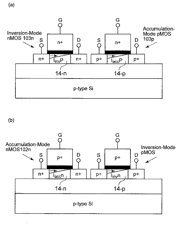
2 n型不純物領域
3a,3b 高濃度p型不純物領域
4a,4b 高濃度p型不純物領域
5 ゲート絶縁膜
6,7 ゲート電極
8 ゲート配線
9 出力配線
10,11 電源配線
12 支持基板
13 埋め込み酸化膜
14 SOI(Silicon on Insulator)層
15 ゲート絶縁膜
16 ゲート電極
17 ソース・ドレイン層(NMOSトランジスタ)
18 ソース・ドレイン層(PMOSトランジスタ)
19 ゲート配線
20 出力配線
21,22 電源配線
Claims (3)
- 一対の異なる導電型のトランジスタを有する回路を備えた半導体装置において、
前記一対の異なる導電型のトランジスタは共にSOI基板に設けたSOI層に形成され、
前記一対の異なる導電型のトランジスタの一方は、前記SOI層の表面の少なくとも一部を覆うゲート絶縁膜と、該ゲート絶縁膜上に形成され、前記SOI層と反対の導電型の高濃度層によって形成されたゲート電極とを含んでノーマリオフのアキュムレーション型として形成され、前記ゲート電極の材料及び前記SOI層の不純物濃度が、前記ゲート電極と前記SOI層との仕事関数差により前記SOI層に形成される空乏層の厚さが前記SOI層の膜厚よりも大きくなるように選択されており、
前記一対の異なる導電型のトランジスタの他方は、前記SOI層の表面の少なくとも一部を覆うゲート絶縁膜と、該ゲート絶縁膜上に形成されたゲート電極とを含んで形成され、
前記一対の異なる導電型のトランジスタの一方はn型MOSFETであり、
前記一対の異なるトランジスタが形成される前記SOI層は同一の導電型と不純物濃度を有し、さらに、(110)面から±10°以内に傾けた面を有することを特徴とする半導体装置。 - 前記ゲート電極の下側に形成されているゲート絶縁膜が、マイクロ波励起のプラズマで形成されたSiO2,Si3N4および金属シリコン合金の酸化膜、金属シリコン合金の窒化膜を少なくとも一種類、含有することを特徴とする請求項1に記載の半導体装置。
- 前記ゲート絶縁膜が600℃以下の温度で形成されたことを特徴とする請求項2に記載の半導体装置。
Priority Applications (7)
| Application Number | Priority Date | Filing Date | Title |
|---|---|---|---|
| JP2005349857A JP5128064B2 (ja) | 2005-06-17 | 2005-12-02 | 半導体装置 |
| EP06757382A EP1906440A4 (en) | 2005-06-17 | 2006-06-16 | SEMICONDUCTOR COMPONENT |
| CN200680018680A CN100595896C (zh) | 2005-06-17 | 2006-06-16 | 半导体装置 |
| KR1020077029218A KR101247876B1 (ko) | 2005-06-17 | 2006-06-16 | 반도체 장치 |
| PCT/JP2006/312098 WO2006135039A1 (ja) | 2005-06-17 | 2006-06-16 | 半導体装置 |
| US11/922,197 US7898033B2 (en) | 2005-06-17 | 2006-06-16 | Semiconductor device |
| TW095121893A TWI394232B (zh) | 2005-06-17 | 2006-06-19 | 半導體裝置 |
Applications Claiming Priority (3)
| Application Number | Priority Date | Filing Date | Title |
|---|---|---|---|
| JP2005177613 | 2005-06-17 | ||
| JP2005177613 | 2005-06-17 | ||
| JP2005349857A JP5128064B2 (ja) | 2005-06-17 | 2005-12-02 | 半導体装置 |
Publications (2)
| Publication Number | Publication Date |
|---|---|
| JP2007027677A JP2007027677A (ja) | 2007-02-01 |
| JP5128064B2 true JP5128064B2 (ja) | 2013-01-23 |
Family
ID=37532392
Family Applications (1)
| Application Number | Title | Priority Date | Filing Date |
|---|---|---|---|
| JP2005349857A Expired - Fee Related JP5128064B2 (ja) | 2005-06-17 | 2005-12-02 | 半導体装置 |
Country Status (7)
| Country | Link |
|---|---|
| US (1) | US7898033B2 (ja) |
| EP (1) | EP1906440A4 (ja) |
| JP (1) | JP5128064B2 (ja) |
| KR (1) | KR101247876B1 (ja) |
| CN (1) | CN100595896C (ja) |
| TW (1) | TWI394232B (ja) |
| WO (1) | WO2006135039A1 (ja) |
Families Citing this family (17)
| Publication number | Priority date | Publication date | Assignee | Title |
|---|---|---|---|---|
| JP5329024B2 (ja) | 2006-06-27 | 2013-10-30 | 国立大学法人東北大学 | 半導体装置 |
| JP2009076890A (ja) * | 2007-08-31 | 2009-04-09 | Semiconductor Energy Lab Co Ltd | 半導体装置の作製方法、半導体装置、及び電子機器 |
| JP5041154B2 (ja) * | 2007-11-19 | 2012-10-03 | ルネサスエレクトロニクス株式会社 | 高周波スイッチ回路 |
| JP5299752B2 (ja) * | 2008-04-28 | 2013-09-25 | 国立大学法人東北大学 | 半導体装置 |
| US7994577B2 (en) | 2008-07-18 | 2011-08-09 | Taiwan Semiconductor Manufacturing Company, Ltd. | ESD protection structures on SOI substrates |
| JP5593107B2 (ja) | 2009-04-02 | 2014-09-17 | 株式会社半導体エネルギー研究所 | 半導体装置の作製方法 |
| US8957462B2 (en) * | 2010-12-09 | 2015-02-17 | Semiconductor Energy Laboratory Co., Ltd. | Semiconductor device comprising an N-type transistor with an N-type semiconductor containing nitrogen as a gate |
| JP2013012768A (ja) * | 2012-09-05 | 2013-01-17 | Tohoku Univ | 半導体装置 |
| FR2999802A1 (fr) | 2012-12-14 | 2014-06-20 | St Microelectronics Sa | Cellule cmos realisee dans une technologie fd soi |
| KR20160055784A (ko) * | 2013-09-27 | 2016-05-18 | 인텔 코포레이션 | 공통 기판 상의 상이한 일함수를 가지는 비-평면 i/o 및 논리 반도체 디바이스들 |
| US9209304B2 (en) * | 2014-02-13 | 2015-12-08 | Taiwan Semiconductor Manufacturing Co., Ltd. | N/P MOS FinFET performance enhancement by specific orientation surface |
| JP6543392B2 (ja) * | 2018-06-29 | 2019-07-10 | ルネサスエレクトロニクス株式会社 | 半導体装置 |
| CN112687689A (zh) * | 2020-12-10 | 2021-04-20 | 西安电子科技大学 | 一种fd cmos结构及其制备方法 |
| WO2022057132A1 (zh) * | 2020-09-18 | 2022-03-24 | 西安电子科技大学 | CMOS结构及FinFET CMOS、FD CMOS、GAA CMOS的制备方法 |
| US20230223408A1 (en) * | 2020-09-18 | 2023-07-13 | Xidian University | Cmos structure, and fabrication methods of finfet cmos, fd cmos and gaa cmos |
| CN112349717B (zh) * | 2020-09-18 | 2023-02-10 | 西安电子科技大学 | 一种FinFET CMOS结构及其制备方法 |
| CN112713191A (zh) * | 2020-12-23 | 2021-04-27 | 张鹤鸣 | 一种环栅纳米cmos结构及其制备方法 |
Family Cites Families (15)
| Publication number | Priority date | Publication date | Assignee | Title |
|---|---|---|---|---|
| US3958266A (en) * | 1974-04-19 | 1976-05-18 | Rca Corporation | Deep depletion insulated gate field effect transistors |
| JPS54158848A (en) * | 1978-06-06 | 1979-12-15 | Nippon Precision Circuits | Semiconductor circuit device |
| US5111260A (en) * | 1983-06-17 | 1992-05-05 | Texax Instruments Incorporated | Polysilicon FETs |
| JPS6170748A (ja) * | 1984-09-14 | 1986-04-11 | Hitachi Ltd | 半導体装置 |
| US4768076A (en) * | 1984-09-14 | 1988-08-30 | Hitachi, Ltd. | Recrystallized CMOS with different crystal planes |
| JPS6292361A (ja) * | 1985-10-17 | 1987-04-27 | Toshiba Corp | 相補型半導体装置 |
| JP3038939B2 (ja) * | 1991-02-08 | 2000-05-08 | 日産自動車株式会社 | 半導体装置 |
| JPH04367278A (ja) * | 1991-06-14 | 1992-12-18 | Canon Inc | 絶縁ゲート薄膜トランジスタ及びその製造方法 |
| JP3248791B2 (ja) | 1993-09-14 | 2002-01-21 | 三菱電機株式会社 | 半導体装置 |
| JP2003115587A (ja) * | 2001-10-03 | 2003-04-18 | Tadahiro Omi | <110>方位のシリコン表面上に形成された半導体装置およびその製造方法 |
| JP2003209258A (ja) * | 2002-01-17 | 2003-07-25 | National Institute Of Advanced Industrial & Technology | 電界効果トランジスタ |
| JP3634320B2 (ja) * | 2002-03-29 | 2005-03-30 | 株式会社東芝 | 半導体装置及び半導体装置の製造方法 |
| US6911383B2 (en) * | 2003-06-26 | 2005-06-28 | International Business Machines Corporation | Hybrid planar and finFET CMOS devices |
| WO2005020325A1 (ja) * | 2003-08-26 | 2005-03-03 | Nec Corporation | 半導体装置及びその製造方法 |
| JP3792694B2 (ja) * | 2003-12-08 | 2006-07-05 | セイコーエプソン株式会社 | 液晶表示装置 |
-
2005
- 2005-12-02 JP JP2005349857A patent/JP5128064B2/ja not_active Expired - Fee Related
-
2006
- 2006-06-16 US US11/922,197 patent/US7898033B2/en not_active Expired - Fee Related
- 2006-06-16 WO PCT/JP2006/312098 patent/WO2006135039A1/ja not_active Ceased
- 2006-06-16 EP EP06757382A patent/EP1906440A4/en not_active Withdrawn
- 2006-06-16 CN CN200680018680A patent/CN100595896C/zh not_active Expired - Fee Related
- 2006-06-16 KR KR1020077029218A patent/KR101247876B1/ko not_active Expired - Fee Related
- 2006-06-19 TW TW095121893A patent/TWI394232B/zh not_active IP Right Cessation
Also Published As
| Publication number | Publication date |
|---|---|
| CN100595896C (zh) | 2010-03-24 |
| TWI394232B (zh) | 2013-04-21 |
| US20090321832A1 (en) | 2009-12-31 |
| KR101247876B1 (ko) | 2013-03-26 |
| KR20080024129A (ko) | 2008-03-17 |
| US7898033B2 (en) | 2011-03-01 |
| CN101203946A (zh) | 2008-06-18 |
| EP1906440A4 (en) | 2011-06-01 |
| WO2006135039A1 (ja) | 2006-12-21 |
| JP2007027677A (ja) | 2007-02-01 |
| TW200709340A (en) | 2007-03-01 |
| EP1906440A1 (en) | 2008-04-02 |
Similar Documents
| Publication | Publication Date | Title |
|---|---|---|
| JP5128064B2 (ja) | 半導体装置 | |
| JP4664631B2 (ja) | 半導体装置及びその製造方法 | |
| US7804132B2 (en) | Semiconductor device | |
| KR101269926B1 (ko) | 반도체 장치 | |
| CN100446271C (zh) | 场效应晶体管 | |
| US20070241400A1 (en) | Semiconductor device | |
| JPWO2005020325A1 (ja) | 半導体装置及びその製造方法 | |
| JP2013191760A (ja) | 半導体装置 | |
| US7863713B2 (en) | Semiconductor device | |
| US20200006489A1 (en) | MOSFET Having Drain Region Formed Between Two Gate Electrodes with Body Contact Region and Source Region Formed in a Double Well Region | |
| US8941186B2 (en) | Semiconductor device having vertical type transistor | |
| JP4457209B2 (ja) | 絶縁ゲート薄膜トランジスタとその制御方法 | |
| JP2001203357A (ja) | 半導体装置 | |
| JP4457218B2 (ja) | 絶縁ゲート薄膜トランジスタ | |
| JP2004235438A (ja) | Soi構造mos型半導体装置及びその製造方法 | |
| JP2007149853A (ja) | 半導体装置およびその製造方法 |
Legal Events
| Date | Code | Title | Description |
|---|---|---|---|
| A621 | Written request for application examination |
Free format text: JAPANESE INTERMEDIATE CODE: A621 Effective date: 20080820 |
|
| A131 | Notification of reasons for refusal |
Free format text: JAPANESE INTERMEDIATE CODE: A131 Effective date: 20120125 |
|
| A521 | Request for written amendment filed |
Free format text: JAPANESE INTERMEDIATE CODE: A523 Effective date: 20120307 |
|
| A131 | Notification of reasons for refusal |
Free format text: JAPANESE INTERMEDIATE CODE: A131 Effective date: 20120801 |
|
| A521 | Request for written amendment filed |
Free format text: JAPANESE INTERMEDIATE CODE: A523 Effective date: 20120816 |
|
| TRDD | Decision of grant or rejection written | ||
| A01 | Written decision to grant a patent or to grant a registration (utility model) |
Free format text: JAPANESE INTERMEDIATE CODE: A01 Effective date: 20121010 |
|
| A01 | Written decision to grant a patent or to grant a registration (utility model) |
Free format text: JAPANESE INTERMEDIATE CODE: A01 |
|
| A61 | First payment of annual fees (during grant procedure) |
Free format text: JAPANESE INTERMEDIATE CODE: A61 Effective date: 20121031 |
|
| R150 | Certificate of patent or registration of utility model |
Free format text: JAPANESE INTERMEDIATE CODE: R150 |
|
| FPAY | Renewal fee payment (event date is renewal date of database) |
Free format text: PAYMENT UNTIL: 20151109 Year of fee payment: 3 |
|
| R250 | Receipt of annual fees |
Free format text: JAPANESE INTERMEDIATE CODE: R250 |
|
| R250 | Receipt of annual fees |
Free format text: JAPANESE INTERMEDIATE CODE: R250 |
|
| R250 | Receipt of annual fees |
Free format text: JAPANESE INTERMEDIATE CODE: R250 |
|
| LAPS | Cancellation because of no payment of annual fees |