EP2040332A1 - Antenne à large bande résonante multimode - Google Patents
Antenne à large bande résonante multimode Download PDFInfo
- Publication number
- EP2040332A1 EP2040332A1 EP08008563A EP08008563A EP2040332A1 EP 2040332 A1 EP2040332 A1 EP 2040332A1 EP 08008563 A EP08008563 A EP 08008563A EP 08008563 A EP08008563 A EP 08008563A EP 2040332 A1 EP2040332 A1 EP 2040332A1
- Authority
- EP
- European Patent Office
- Prior art keywords
- length
- cutouts
- edge
- electromagnetic wave
- receive unit
- Prior art date
- Legal status (The legal status is an assumption and is not a legal conclusion. Google has not performed a legal analysis and makes no representation as to the accuracy of the status listed.)
- Withdrawn
Links
- 239000002184 metal Substances 0.000 claims abstract description 19
- 238000000034 method Methods 0.000 claims abstract description 7
- 238000005452 bending Methods 0.000 claims description 15
- 230000005684 electric field Effects 0.000 claims description 13
- 238000005520 cutting process Methods 0.000 claims description 7
- 239000000758 substrate Substances 0.000 claims description 7
- 230000005540 biological transmission Effects 0.000 claims description 2
- 238000005530 etching Methods 0.000 claims description 2
- 238000010586 diagram Methods 0.000 description 6
- 238000004519 manufacturing process Methods 0.000 description 3
- 230000008901 benefit Effects 0.000 description 2
- 230000007423 decrease Effects 0.000 description 2
- 230000003247 decreasing effect Effects 0.000 description 2
- 230000007812 deficiency Effects 0.000 description 2
- 238000012986 modification Methods 0.000 description 2
- 230000004048 modification Effects 0.000 description 2
- 230000008878 coupling Effects 0.000 description 1
- 230000001808 coupling effect Effects 0.000 description 1
- 238000010168 coupling process Methods 0.000 description 1
- 238000005859 coupling reaction Methods 0.000 description 1
- 238000005516 engineering process Methods 0.000 description 1
- 230000005404 monopole Effects 0.000 description 1
Images


Classifications
-
- H—ELECTRICITY
- H01—ELECTRIC ELEMENTS
- H01Q—ANTENNAS, i.e. RADIO AERIALS
- H01Q1/00—Details of, or arrangements associated with, antennas
- H01Q1/36—Structural form of radiating elements, e.g. cone, spiral, umbrella; Particular materials used therewith
-
- H—ELECTRICITY
- H01—ELECTRIC ELEMENTS
- H01Q—ANTENNAS, i.e. RADIO AERIALS
- H01Q9/00—Electrically-short antennas having dimensions not more than twice the operating wavelength and consisting of conductive active radiating elements
- H01Q9/04—Resonant antennas
- H01Q9/30—Resonant antennas with feed to end of elongated active element, e.g. unipole
- H01Q9/40—Element having extended radiating surface
-
- H—ELECTRICITY
- H01—ELECTRIC ELEMENTS
- H01Q—ANTENNAS, i.e. RADIO AERIALS
- H01Q9/00—Electrically-short antennas having dimensions not more than twice the operating wavelength and consisting of conductive active radiating elements
- H01Q9/04—Resonant antennas
- H01Q9/30—Resonant antennas with feed to end of elongated active element, e.g. unipole
- H01Q9/42—Resonant antennas with feed to end of elongated active element, e.g. unipole with folded element, the folded parts being spaced apart a small fraction of the operating wavelength
Definitions
- the present invention relates to a wideband antenna and a manufacturing method for the same, and more particularly to a multi-mode resonant wideband antenna and a manufacturing method for the same.
- the application of antenna in wireless LAN card is not only limited by the character of the antenna, but also by the space and the cost of the wireless LAN card.
- the chip antenna is usually applied in the wireless LAN card because of its small size.
- the chip antenna has the deficiencies of the high cost and the narrow bandwidth.
- the real bandwidth thereof is often narrower than expected because of the interference from the printed circuit board (PCB) layout.
- the printed antennas include the monopole antenna, the dipole antenna, the planar inverted-F antenna, and the ring antenna, characterized in that the planar inverted-F antenna is frequently used because it could efficiently reduce the size occupied by the printed antenna on PCB. Nevertheless, the bandwidth of the planar inverted-F antenna is always limited by the special structure itself. If the bandwidth of an antenna is not broad enough, the most electromagnetic wave delivered by the antenna would easily be reflected back by the surrounding objects that are close to the antenna. Further, the character of the return loss of the antenna is possible to be affected, which makes the deviation of the central frequency. For overcoming these deficiencies, an antenna that could provide a broader bandwidth and a better performance in return loss, and could overcome the affection of the surrounding objects to the return loss and the central frequency deviation, without any additional cost, is needed.
- a multi-mode resonant wideband antenna and a manufacturing method for the same are provided.
- the particular design in the present invention not only solves the problems described above, but also is easy to be implemented.
- the invention has the utility for the industry.
- a wireless transmit/receive unit for transmitting and receiving an electromagnetic wave.
- the wireless transmit/receive unit includes a radiating element (11) and a feeding line (12).
- the radiating element (11) is a metal piece having a first edge (113) with a first length, a second edge (114) with a second length, and a plurality of cutouts (111a-111e).
- the first edge (113) and the second edge (114) are separated from each other and the first length is longer than the second length.
- the cutouts (111a-111e) are formed on the metal piece and make the metal piece have a zigzag shape.
- the feeding line (12) is electrically connected to the second edge (114).
- the metal piece is an inverted triangle-shaped metal plate or an inverted trapezium-shaped metal plate, and the metal piece has an effective electrical length that is a multiple of a half wavelength of the electromagnetic wave.
- the first length is a multiple of a quarter wavelength of the electromagnetic wave and the cutouts (111a-111e) being cutting slots have a total length that is a multiple of a half wavelength of the electromagnetic wave.
- each of the cutouts (111 a-111e) being cutting slots has a width of 20 milliinches.
- the wireless transmit/receive unit further includes a reference ground surface (14) coupled to a dielectric substrate (13), and the feeding line (12) is mounted on the dielectric substrate (13) made of an FR4 laminate.
- the wireless transmit/receive unit is configured in a wireless transmission device.
- the radiating element (11) is a meander line (112) having a first terminal (115) and a second terminal (116).
- the meander line (112) includes a first section (112e), a second section (112d), a third section (112a), a first bending part (117), and a second bending part (118).
- the first section (112e) has a first length and is connected to the first terminal (115), and the second section (112d) has a second length and is connected to the first section (112e) via the first bending part (117).
- the third section (112a) has a third length and is connected at one end to the second section (112d) via the second bend part (118) and is connected at another end to the second terminal (116). Further, the first length is shorter than the second length, and the second length is shorter than the third length.
- the feeding line (12) is electrically connected to the first terminal (115).
- the third length is a multiple of a quarter wavelength of the electromagnetic wave and the meander line (112) has a total length that is a multiple of a half wavelength of the electromagnetic wave.
- a method for increasing a bandwidth of an antenna includes steps as follows.
- the first step is to provide a radiating element (11) that has a first edge (113) with a first length and a second edge (114) with a second length, where the first length is longer than the second length.
- the second step is to form a plurality of cutouts (111a-111e) on the radiating element (11) for producing a plurality of horizontal electric fields parallel to the cutouts (111a-111e) and a plurality of perpendicular electric fields perpendicular to the cutouts (111a-111e), where the horizontal electric fields offset with each other and the perpendicular electric fields superimpose with each other.
- the cutouts (111a-111e) are formed by one of a cutting process and an etching process.
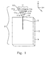
- Fig. 1 is an illustrating diagram showing a multi-mode resonant wideband antenna according to the first preferred embodiment of the present invention
- Fig. 2 is an illustrating diagram showing a radiating element according to the second preferred embodiment of the present invention.
- Fig. 3A is a polar graph showing an horizontal field pattern of the multi-mode resonant wideband antenna in the XZ plane according to the first preferred embodiment of the present invention
- Fig. 3B is a polar graph showing an perpendicular field pattern of the multi-mode resonant wideband antenna in the XZ plane according to the first preferred embodiment of the present invention
- Fig. 4A is a polar graph showing an horizontal field pattern of the multi-mode resonant wideband antenna in the XY plane according to the first preferred embodiment of the present invention
- Fig. 4B is a polar graph showing an perpendicular field pattern of the multi-mode resonant wideband antenna in the XY plane according to the first preferred embodiment of the present invention.
- Fig. 5 is a diagram showing the return loss of the multi-mode resonant wideband antenna in different frequencies according to the first preferred embodiment of the present invention.
- the multi-mode resonant wideband antenna 01 of the present invention includes a radiating element 11, a feeding line 12, a dielectric substrate 13, and a reference ground surface 14.
- the radiating element 11 is formed from a metal piece having a shape of inverted triangle, and the metal piece has a first edge 113, a second edge 114, plural sections 112a-112e (of which only 112a is marked in Fig. 1 ) and plural cutouts 111a-111e.
- the number of cutouts could vary based on necessary in practice, as well as five cutouts 111a-111e exist in our embodiment.
- the respective cutouts 111a-111e have successively decreasing lengths, which makes the radiating element 11 have a zigzag shape.
- the dielectric substrate 13 is a FR4 substrate.
- the length of the edges of the radiating element 11 and each of the cutouts 111a-111e could be adjusted accordingly.
- the first edge 113 has a length equal to a quarter wavelength of the electromagnetic wave having a frequency of 2.45GHz
- the respective cutouts 111a-111e have a width of 20 milliinches, which is easy to be carried out by the present technology.
- the sum of the length of the respective sections 112a-112e is equal to a half wavelength of the electromagnetic wave having a frequency of 2.45GHz.
- the radiating element 11 includes a meander line 112 connected to the feeding line 12, and plural cutouts 111a-111e (of which only cutting slot 111a is marked in Fig. 2 ).
- the meander line 112 further includes a first terminal 115, a second terminal 116, plural sections 112a-112e (of which only 112a, 112d and 112e are shown in Fig. 2 ), and plural bending parts 117-121. As showed in Fig.
- the current would be transmitted from the first terminal 115 to the second terminal 116 via the meander line 112, which not only makes the respective sections 112a-112e have an individual horizontal electric field (-x/+x) but also makes each bending part 117-121 have a perpendicular electric field (+y).
- the horizontal electric fields of the respective sections 112a-112e would offset each other because of the alternatively opposite directions (-x/+x) thereof, and the perpendicular electric fields of each bending part 117-121 would superimpose each other because of the same direction (+y) thereof.
- Figs. 3A and 3B are polar graphs showing a horizontal and a perpendicular field patterns of the multi-mode resonant wideband antenna in the XZ plane according to the first preferred embodiment of the present invention. As the Fig. 3B shows, the sum of the electric fields in the perpendicular direction (+y) make the invented antenna being an omnidirectional antenna in XZ plane.
- Figs. 4A and 4B are polar graphs showing a horizontal and a perpendicular field patterns of the multi-mode resonant wideband antenna in the XY plane according to the first preferred embodiment of the present invention. Because the cutouts 111a-111e have very narrow widths (20 milliinches), the respective sections 112a-112e have relatively broad widths, which decreases the impedance of the radiating element 11 and improves the invented antenna performance. As the Fig. 4A shows, the antenna of the present invention has an ideal performance of 3 dBi peak gain in the XY plane.
- the cutouts 111a-111e have very narrow widths (20 milliinches), the multiple leakage currents would be induced easily across each cutouts 111a-111e, which makes the radiating element 11 have multiple effective electrical lengths from a quarter to a half wavelength of the received electromagnetic wave. Therefore, by coupling multiple effective electrical lengths, a broader bandwidth could be easily provided.
- Fig. 5 is a diagram showing the return loss of the multi-mode resonant wideband antenna according to the first preferred embodiment of the present invention.
- the y-axis presents the return loss
- the x-axis presents the operating frequencies.
- the radiating element 11 has an effective electrical length equal to a half wavelength of the received electromagnetic wave, which makes the radiating element 11 have a high perpendicular current in the bending part 120.
- a corresponding resonant frequency of 2.4 GHz could be found in Fig. 5 , which is labeled as mark 1.
- the bending part 120 is far away form the reference ground surface 14, which could decrease the interference induced by the ground 14.
- an effective electrical length equal to a quarter wavelength of the received electromagnetic wave would make the radiating element 11 have a high perpendicular current in the bending part 117.
- a corresponding resonant frequency of 2.5 GHz that is labeled as mark 3 could also be found in Fig. 5 .
- the triangle-shaped radiating element 11 has the benefit of decreasing the coupling effect existing between the radiating element 11 and the reference ground surface 14.
- the bandwidth of the invented antenna is 200 MHz.
- the bandwidth of the invented antenna is 600 MHz.
Landscapes
- Details Of Aerials (AREA)
- Waveguide Aerials (AREA)
- Support Of Aerials (AREA)
Applications Claiming Priority (1)
| Application Number | Priority Date | Filing Date | Title |
|---|---|---|---|
| TW096135232A TWI347710B (en) | 2007-09-20 | 2007-09-20 | Multi-mode resonator broadband antenna |
Publications (1)
| Publication Number | Publication Date |
|---|---|
| EP2040332A1 true EP2040332A1 (fr) | 2009-03-25 |
Family
ID=39876620
Family Applications (1)
| Application Number | Title | Priority Date | Filing Date |
|---|---|---|---|
| EP08008563A Withdrawn EP2040332A1 (fr) | 2007-09-20 | 2008-05-07 | Antenne à large bande résonante multimode |
Country Status (5)
| Country | Link |
|---|---|
| US (1) | US20090079659A1 (fr) |
| EP (1) | EP2040332A1 (fr) |
| JP (1) | JP2009077369A (fr) |
| CA (1) | CA2625388A1 (fr) |
| TW (1) | TWI347710B (fr) |
Families Citing this family (4)
| Publication number | Priority date | Publication date | Assignee | Title |
|---|---|---|---|---|
| US10264637B2 (en) * | 2009-09-24 | 2019-04-16 | Cree, Inc. | Solid state lighting apparatus with compensation bypass circuits and methods of operation thereof |
| JP2013187614A (ja) * | 2012-03-06 | 2013-09-19 | Yamaha Corp | アンテナ |
| TWI552442B (zh) | 2014-07-16 | 2016-10-01 | 啟碁科技股份有限公司 | 雙頻天線 |
| CN106848559B (zh) * | 2017-02-15 | 2023-07-25 | 河南师范大学 | 一种共面波导馈电的多频天线 |
Citations (4)
| Publication number | Priority date | Publication date | Assignee | Title |
|---|---|---|---|---|
| US5986609A (en) * | 1998-06-03 | 1999-11-16 | Ericsson Inc. | Multiple frequency band antenna |
| WO2001093370A1 (fr) * | 2000-05-31 | 2001-12-06 | Bae Systems Information And Electronic Systems Integration Inc. | Antenne chargee de structure en meandres, polarisee de maniere circulaire, croisee, symetrique, et a bande etroite |
| EP1729367A1 (fr) * | 2004-03-22 | 2006-12-06 | Yokowo Co., Ltd | Antenne repli e |
| US20070132658A1 (en) * | 2001-10-16 | 2007-06-14 | Ramiro Quintero Illera | Multiband antenna |
Family Cites Families (9)
| Publication number | Priority date | Publication date | Assignee | Title |
|---|---|---|---|---|
| US3369243A (en) * | 1965-01-18 | 1968-02-13 | Univ Illinois | Log-periodic antenna structure |
| GB2330951B (en) * | 1997-11-04 | 2002-09-18 | Nokia Mobile Phones Ltd | Antenna |
| KR100285950B1 (ko) * | 1997-12-26 | 2001-04-16 | 윤종용 | 인체의영향을최소화시키는휴대용전화기의안테나회로를구현하는방법 |
| JP3469880B2 (ja) * | 2001-03-05 | 2003-11-25 | ソニー株式会社 | アンテナ装置 |
| US6661380B1 (en) * | 2002-04-05 | 2003-12-09 | Centurion Wireless Technologies, Inc. | Multi-band planar antenna |
| JP2004247790A (ja) * | 2003-02-10 | 2004-09-02 | Ngk Spark Plug Co Ltd | 逆fアンテナ |
| SE0302175D0 (sv) * | 2003-08-07 | 2003-08-07 | Kildal Antenna Consulting Ab | Broadband multi-dipole antenna with frequencyindependent radiation characteristics |
| EP1564842B1 (fr) * | 2004-02-17 | 2017-12-20 | Orange | Antenne ultra large bande |
| US7358925B2 (en) * | 2004-10-07 | 2008-04-15 | Sony Ericsson Mobile Communications Ab | Highly-integrated headset |
-
2007
- 2007-09-20 TW TW096135232A patent/TWI347710B/zh not_active IP Right Cessation
-
2008
- 2008-01-14 US US12/013,516 patent/US20090079659A1/en not_active Abandoned
- 2008-03-06 JP JP2008056490A patent/JP2009077369A/ja active Pending
- 2008-03-12 CA CA002625388A patent/CA2625388A1/fr not_active Abandoned
- 2008-05-07 EP EP08008563A patent/EP2040332A1/fr not_active Withdrawn
Patent Citations (4)
| Publication number | Priority date | Publication date | Assignee | Title |
|---|---|---|---|---|
| US5986609A (en) * | 1998-06-03 | 1999-11-16 | Ericsson Inc. | Multiple frequency band antenna |
| WO2001093370A1 (fr) * | 2000-05-31 | 2001-12-06 | Bae Systems Information And Electronic Systems Integration Inc. | Antenne chargee de structure en meandres, polarisee de maniere circulaire, croisee, symetrique, et a bande etroite |
| US20070132658A1 (en) * | 2001-10-16 | 2007-06-14 | Ramiro Quintero Illera | Multiband antenna |
| EP1729367A1 (fr) * | 2004-03-22 | 2006-12-06 | Yokowo Co., Ltd | Antenne repli e |
Also Published As
| Publication number | Publication date |
|---|---|
| CA2625388A1 (fr) | 2009-03-20 |
| TW200915665A (en) | 2009-04-01 |
| TWI347710B (en) | 2011-08-21 |
| JP2009077369A (ja) | 2009-04-09 |
| US20090079659A1 (en) | 2009-03-26 |
Similar Documents
| Publication | Publication Date | Title |
|---|---|---|
| TWI425713B (zh) | 諧振產生之三頻段天線 | |
| US6774850B2 (en) | Broadband couple-fed planar antennas with coupled metal strips on the ground plane | |
| EP2065972B1 (fr) | Antenne à double bande | |
| US6788266B2 (en) | Diversity slot antenna | |
| US8648762B2 (en) | Loop array antenna system and electronic apparatus having the same | |
| US7649501B2 (en) | Ultra-wideband antenna structure | |
| US20090128439A1 (en) | Dipole antenna device and dipole antenna system | |
| US20100253580A1 (en) | Printed antenna and electronic device employing the same | |
| US7911390B2 (en) | Antenna structure | |
| US9368858B2 (en) | Internal LC antenna for wireless communication device | |
| US7183981B1 (en) | Monopole antenna | |
| CN106450726A (zh) | 一种宽带开槽端射微带天线 | |
| AU2021327073A9 (en) | Miniature antenna with omnidirectional radiation field | |
| EP2840652B1 (fr) | Antenne | |
| EP2040332A1 (fr) | Antenne à large bande résonante multimode | |
| US20120326940A1 (en) | Multi-band antenna and electronic apparatus having the same | |
| US9130276B2 (en) | Antenna device | |
| US8059042B2 (en) | Shorted monopole antenna | |
| CN101409381A (zh) | 无线传输/接收单元与宽频天线及增加天线频宽方法 | |
| KR100714201B1 (ko) | 초 광대역 안테나 | |
| CN114094327B (zh) | 一种天线结构及终端 | |
| US20080284657A1 (en) | Meandered Antenna | |
| CN110534882A (zh) | 一种双频天线 | |
| US20070126640A1 (en) | Planar antenna structure | |
| JP5112192B2 (ja) | アンテナ、ならびに、rfidリーダ |
Legal Events
| Date | Code | Title | Description |
|---|---|---|---|
| PUAI | Public reference made under article 153(3) epc to a published international application that has entered the european phase |
Free format text: ORIGINAL CODE: 0009012 |
|
| 17P | Request for examination filed |
Effective date: 20080515 |
|
| AK | Designated contracting states |
Kind code of ref document: A1 Designated state(s): AT BE BG CH CY CZ DE DK EE ES FI FR GB GR HR HU IE IS IT LI LT LU LV MC MT NL NO PL PT RO SE SI SK TR |
|
| AX | Request for extension of the european patent |
Extension state: AL BA MK RS |
|
| 17Q | First examination report despatched |
Effective date: 20090826 |
|
| AKX | Designation fees paid |
Designated state(s): DE FR GB IT |
|
| STAA | Information on the status of an ep patent application or granted ep patent |
Free format text: STATUS: THE APPLICATION HAS BEEN WITHDRAWN |
|
| 18W | Application withdrawn |
Effective date: 20100310 |