EP2040525A2 - Elektronische Vorrichtung mit Leiterplatte, Steckverbinder und Gehäuse - Google Patents
Elektronische Vorrichtung mit Leiterplatte, Steckverbinder und Gehäuse Download PDFInfo
- Publication number
- EP2040525A2 EP2040525A2 EP08014452A EP08014452A EP2040525A2 EP 2040525 A2 EP2040525 A2 EP 2040525A2 EP 08014452 A EP08014452 A EP 08014452A EP 08014452 A EP08014452 A EP 08014452A EP 2040525 A2 EP2040525 A2 EP 2040525A2
- Authority
- EP
- European Patent Office
- Prior art keywords
- case
- housing
- engaging
- wall
- circuit board
- Prior art date
- Legal status (The legal status is an assumption and is not a legal conclusion. Google has not performed a legal analysis and makes no representation as to the accuracy of the status listed.)
- Granted
Links
- 230000003247 decreasing effect Effects 0.000 claims description 5
- 230000004048 modification Effects 0.000 description 12
- 238000012986 modification Methods 0.000 description 12
- 230000008878 coupling Effects 0.000 description 7
- 238000010168 coupling process Methods 0.000 description 7
- 238000005859 coupling reaction Methods 0.000 description 7
- 230000000052 comparative effect Effects 0.000 description 6
- 230000008859 change Effects 0.000 description 4
- 230000007423 decrease Effects 0.000 description 3
- 238000003780 insertion Methods 0.000 description 3
- 230000037431 insertion Effects 0.000 description 3
- 229920005989 resin Polymers 0.000 description 3
- 239000011347 resin Substances 0.000 description 3
- 229910000679 solder Inorganic materials 0.000 description 3
- 239000012141 concentrate Substances 0.000 description 2
- 239000011521 glass Substances 0.000 description 2
- 238000000034 method Methods 0.000 description 2
- 230000008569 process Effects 0.000 description 2
- 238000002834 transmittance Methods 0.000 description 2
- XAGFODPZIPBFFR-UHFFFAOYSA-N aluminium Chemical compound [Al] XAGFODPZIPBFFR-UHFFFAOYSA-N 0.000 description 1
- 229910052782 aluminium Inorganic materials 0.000 description 1
- 239000003990 capacitor Substances 0.000 description 1
- 239000000919 ceramic Substances 0.000 description 1
- 239000004020 conductor Substances 0.000 description 1
- 238000004512 die casting Methods 0.000 description 1
- 230000005611 electricity Effects 0.000 description 1
- 239000004744 fabric Substances 0.000 description 1
- 239000011810 insulating material Substances 0.000 description 1
- 238000000465 moulding Methods 0.000 description 1
- 230000003014 reinforcing effect Effects 0.000 description 1
- 229920005992 thermoplastic resin Polymers 0.000 description 1
- 229920001187 thermosetting polymer Polymers 0.000 description 1
Images





Classifications
-
- H—ELECTRICITY
- H05—ELECTRIC TECHNIQUES NOT OTHERWISE PROVIDED FOR
- H05K—PRINTED CIRCUITS; CASINGS OR CONSTRUCTIONAL DETAILS OF ELECTRIC APPARATUS; MANUFACTURE OF ASSEMBLAGES OF ELECTRICAL COMPONENTS
- H05K5/00—Casings, cabinets or drawers for electric apparatus
- H05K5/0026—Casings, cabinets or drawers for electric apparatus provided with connectors and printed circuit boards [PCB], e.g. automotive electronic control units
- H05K5/0039—Casings, cabinets or drawers for electric apparatus provided with connectors and printed circuit boards [PCB], e.g. automotive electronic control units having a tubular housing wherein the PCB is inserted longitudinally
-
- H—ELECTRICITY
- H01—ELECTRIC ELEMENTS
- H01R—ELECTRICALLY-CONDUCTIVE CONNECTIONS; STRUCTURAL ASSOCIATIONS OF A PLURALITY OF MUTUALLY-INSULATED ELECTRICAL CONNECTING ELEMENTS; COUPLING DEVICES; CURRENT COLLECTORS
- H01R12/00—Structural associations of a plurality of mutually-insulated electrical connecting elements, specially adapted for printed circuits, e.g. printed circuit boards [PCB], flat or ribbon cables, or like generally planar structures, e.g. terminal strips, terminal blocks; Coupling devices specially adapted for printed circuits, flat or ribbon cables, or like generally planar structures; Terminals specially adapted for contact with, or insertion into, printed circuits, flat or ribbon cables, or like generally planar structures
- H01R12/70—Coupling devices
- H01R12/71—Coupling devices for rigid printing circuits or like structures
- H01R12/712—Coupling devices for rigid printing circuits or like structures co-operating with the surface of the printed circuit or with a coupling device exclusively provided on the surface of the printed circuit
- H01R12/716—Coupling device provided on the PCB
-
- H—ELECTRICITY
- H01—ELECTRIC ELEMENTS
- H01R—ELECTRICALLY-CONDUCTIVE CONNECTIONS; STRUCTURAL ASSOCIATIONS OF A PLURALITY OF MUTUALLY-INSULATED ELECTRICAL CONNECTING ELEMENTS; COUPLING DEVICES; CURRENT COLLECTORS
- H01R12/00—Structural associations of a plurality of mutually-insulated electrical connecting elements, specially adapted for printed circuits, e.g. printed circuit boards [PCB], flat or ribbon cables, or like generally planar structures, e.g. terminal strips, terminal blocks; Coupling devices specially adapted for printed circuits, flat or ribbon cables, or like generally planar structures; Terminals specially adapted for contact with, or insertion into, printed circuits, flat or ribbon cables, or like generally planar structures
- H01R12/70—Coupling devices
- H01R12/71—Coupling devices for rigid printing circuits or like structures
- H01R12/72—Coupling devices for rigid printing circuits or like structures coupling with the edge of the rigid printed circuits or like structures
- H01R12/722—Coupling devices for rigid printing circuits or like structures coupling with the edge of the rigid printed circuits or like structures coupling devices mounted on the edge of the printed circuits
- H01R12/724—Coupling devices for rigid printing circuits or like structures coupling with the edge of the rigid printed circuits or like structures coupling devices mounted on the edge of the printed circuits containing contact members forming a right angle
Definitions
- the present invention relates to an electronic device including a printed circuit board, a connector mounted on the printed circuit board, and a casing housing the printed circuit board therein.
- a printed circuit board is housed in a case having an opening portion, and a housing of a connector mounted on the printed circuit board covers the opening portion of the case.
- a case has an approximately rectangular box shape and has an opening portion at one sidewall.
- Each of two sidewalls located on opposite sides of the one sidewall has a fixing hole.
- a connector has two fixing projections each engaging with corresponding one of the fixing holes.
- a unit body including the connector is fixed to the case.
- the one sidewall having the opening portion has engaging ribs protruding to an outside of the case and the connector has engaging grooves.
- Each of the engaging ribs is fitted into corresponding one of the engaging grooves.
- the two sidewalls are restricted from opening toward the outside of the case.
- the engagements of the fixing holes and the fixing projections are restricted from being released.
- center portions of the two sidewalls in a longitudinal direction of the two sidewalls may warp toward the outside of the case due to a change in a temperature.
- the engaging ribs and the engaging projections are difficult to restrict the warps of the two sidewalls.
- the engagements of the fixing holes and the fixing projections are possibly released.
- a case has an approximately rectangular box shape and one side of the case opens to provide an opening portion.
- the case has first fixing parts (holes) adjacent to the opening portion.
- a housing of a connector has second fixing parts (projections) adjacent to the opening portion.
- the opening portion is covered with the housing in a state where each of the second fixing parts engages with corresponding one of the first engaging parts.
- the opening portion is deformed to have an arcuate shape before the housing is inserted therein. By inserting the housing into the opening portion, the shape of the opening portion is adjusted so as to strengthen the engagements of the first fixing parts and the second fixing parts.
- the shape of the opening portion may be deformed and/or sidewalls may warp due to a change in the temperature.
- the engagements of the first engaging parts and the second engaging parts are possibly released due to the deformation of the opening portion or the warps of the sidewalls.
- an object of the present invention to provide an electronic device that includes a case and a connector fixed to each other with a high degree of certainty.
- an electronic device includes a printed circuit board, a case, and a connector.
- the printed circuit board has an electronic element and a plurality of lands.
- the case has an approximately rectangular tubular shape and one end of the approximately rectangular tubular shape opens to provide an opening portion from which the printed circuit board is inserted into the case.
- the connector includes a housing and a plurality of terminals arranged in the housing. The housing covers the opening portion of the case and defines an inner space.
- Each of the plurality of terminals has two end portions. One end portion of the each of the plurality of terminals extends from the housing and is coupled with corresponding one of the plurality of lands. The other end portion of the each of the plurality of terminals extends from the housing toward the inner space.
- the case includes a wall having a case-side fixing part and a case-side engaging part at a portion adjacent to the opening portion.
- the housing has a housing-side fixing part and a housing-side engaging part at a surface facing the wall of the case.
- the case-side fixing part is one of a fixing projection and a fixing hole and the housing-side fixing part is the other one of the fixing projection and the fixing hole.
- the case-side fixing part engages with the housing-side fixing part for fixing the case and the housing to each other.
- the case-side engaging part is one of an engaging projection and an engaged section and the housing-side engaging part is the other one of the engaging projection and the engaged section.
- the case-side engaging part engages with the housing-side engaging part for restricting the portion of the case adjacent to the opening portion from separating from the housing.
- the case and the connector can be fixed to each other at a high degree of certainty due to the engagement of the case-side engaging part and the housing-side engaging part in addition to the engagement of the case-side fixing part and the housing-side fixing part.
- the electronic control device 100 has a non-waterproof structure and can be suitably used for an electronic control device disposed in a vehicle, for example, for an engine electronic control unit (engine ECU).
- engine ECU engine electronic control unit
- the electronic control device 100 includes a printed circuit board 10, a case 30, and a connector 50.
- the case 30 houses the printed circuit board 10 therein.
- the case 30 has an opening portion 34 on one side thereof.
- the connector 50 is mounted on the printed circuit board 10 and covers the opening portion 34 of the case 30.
- the printed circuit board 10 has an approximately rectangular plate shape.
- the printed circuit board 10 has wirings and via holes for coupling the wirings.
- the wirings include lands functioning as electrodes.
- electronic elements (not shown) including a microcomputer, a power transistor, a resistor, and a capacitor are mounted.
- the connector 50 is mounted on the printed circuit board 10 as one of the electronic elements.
- the connector 50 is configured to electrically couple the printed circuit board 10 and an external connector.
- the connector 50 includes a housing 51 and a plurality of terminals 52. Each of the terminals 52 are coupled with corresponding one of the lands through a solder.
- the printed circuit board 10 may be made of thermoplastic resin, thermosetting resin, ceramics, or a complex of glass (e.g., glass fabric) and resin, for example.
- the number of layer of the printed circuit board 10 is not limited.
- the case 30 houses the printed circuit board 10 therein.
- the case 30 may be made of aluminum die casting, press working, or resin molding, for example.
- the case 30 has an approximately rectangular box shape defined by an upper wall 32, a lower wall 33 facing the upper wall 32, and three sidewalls 31 located between the upper wall 32 and the lower wall 33.
- Each of the upper wall 32 and the lower wall 33 is larger than each of the sidewalls 31.
- the upper wall 32, the lower wall 33 and two of the sidewalls 31 define the opening portion 34 on an opposite side of the other one of the sidewall 31.
- the sidewall 31 located on an opposite side of the opening portion 34 is called a rear wall 31a.
- the printed circuit board 10 is inserted into the case 30 from the opening portion 34 toward the rear wall 31a.
- an open edge 35 of the case 30 that defines the opening portion 34 has a taper shape so that the printed circuit board 10 can be easily inserted into the case 30.
- the case 30 has at least one case-side fixing part at a portion adjacent to the opening portion 34. That is, at least one of the upper wall 32, the lower wall 33, and the two sidewalls 31 adjacent to the opening portion 34 has the case-side fixing part at the portion adjacent to the opening portion 34.
- the case-side fixing part engages with a housing-side fixing part formed at the housing 51 so that the case 30 and the housing 51 are fixed to each other in a direction approximately perpendicular to an engaging direction of the fixing parts.
- each of the upper wall 32 and the lower wall 33 has a fixing hole 36 at a middle portion in a longitudinal direction of the housing 51 as an example of the case-side fixing part.
- Each of the fixing holes 36 has an approximately rectangular cross-sectional shape.
- each of the upper wall 32 and the lower wall 33 has a spring groove 37 adjacent to corresponding one of the fixing holes 36.
- Each of the spring grooves 37 has an approximately U-shape and extends from an inner surface to an outer surface of the case 30.
- a portion between each of the fixing holes 36 and corresponding one of the spring grooves 37 becomes a spring section.
- each of the fixing holes 36 is a through hole, as an example.
- Each of the fixing holes 36 may be also a blind hole that does not extend to the outer surface of the case 30.
- At least one of the walls having the case-side fixing part has a case-side engaging part so that the portion of the case 30 adjacent to the opening portion 34 does not separate from the housing 51 in the engaging direction of the fixing parts. That is, the case-side engaging part is provided for restricting the engagement of the fixing parts from being released.
- each of the upper wall 32 and the lower wall 33 has two cutting sections 38 as an example of the case-side engaging part.
- Each of the cutting sections 38 has an approximately rectangular shape and extends from the open edge 35 of the case 30 toward the rear wall 31a in the inserting direction of the printed circuit board 10.
- the two cutting sections 38 of each of the upper wall 32 and the lower wall 33 are arranged to be line symmetry with respect to the fixing hole 36 of the each of the upper wall 32 and the lower wall 33.
- An edge portion 39 of each of the cutting sections 38 includes a base part 39a and a taper part 39b.
- the base part 39a is located from the inner surface of the case 30 to a predetermined distance from the inner surface.
- the base part 39a has a substantially constant width.
- the taper part 39b is located from a boundary with the base part 39a to the outer surface of the case 30. A width of the taper part 39b increases from the boundary with the base part 39a to the outer surface of the case 30.
- the case 30 has contact portions 40 at the inner surface thereof.
- the terminals 52 extend from a rear surface 56 of the housing 51 toward the land.
- each of the contact portions 40 is in contact with corresponding one of longitudinal end portions 56a of the rear surface 56.
- the case 30 has step portions to provide the contact portions 40.
- the contact portions 40 may be also protruding portions that protrude from the inner surface of the case 30 toward inside.
- the contact portions 40 may have other shape as long as the contact portions 40 can function as stoppers.
- the rear wall 31a has a holding groove 41 at an inner surface thereof so as to hold an end of the printed circuit board 10 on the rear wall side, i.e., a rear end of the printed circuit board 10.
- each of the two sidewalls 31 adjacent to the opening portion 34 has a guide groove 42 at an inner surface thereof.
- the guide grooves 42 are configured to guide the printed circuit board 10 to the rear wall side of the case 30.
- the holding groove 41 extends from one end to the other end of the rear wall 31 a in the longitudinal direction of the housing 51.
- the holding groove 41 In a thickness direction of the printed circuit board 10, the holding groove 41 has a substantially constant width.
- Each of the longitudinal ends of the holding groove 41 communicates with corresponding one of the guide grooves 42.
- a width of each of the guide grooves 42 decreases toward the rear wall side of the case 30.
- the width of the holding groove 41 and the width of each of the guide grooves 42 at the communicating portions with the holding groove 41 are substantially equal to or slightly greater than a thickness of the printed circuit board 10.
- each of the guide grooves 42 is larger than the thickness of the printed circuit board 10 at a portion adjacent to a front end of the printed circuit board 10 located on an opposite side of the rear end.
- the terminals 52 of the connector 50 are coupled with the lands.
- the printed circuit board 10 is away from the guide grooves 42 at the portion adjacent to the front end.
- the connector 50 includes the housing 51 and the terminals 52 arranged in the housing 51.
- the housing 51 is made of an insulating material.
- the terminals 52 are made of a conductive material.
- the connector 50 is mounted on the portion of the printed circuit board 10 adjacent to the front end.
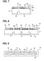
- the housing 51 is configured to cover the opening portion 34 of the case 30. As illustrated in FIG. 1, FIG. 2 , and FIG. 10 , a portion of the housing 51 disposed in the case 30 has an approximately rectangular contour corresponding to an approximately rectangular opening portion 34 defined by the open edge 35. In addition, as illustrated in FIG. 1 , FIG. 9 , and FIG. 10 , another portion of the housing 51 that is in contact with the open edge 35 and is exposed to an outside of the case 30 has an approximately rectangular contour corresponding to the approximately rectangular opening portion 34.
- the housing 51 has a protruding portion 53 that protrudes to the outside with respect to the portion of the housing 51 disposed in the case 30.
- the protruding portion 53 has a ring shape so that the protruding portion 53 is in contact with the whole circumference of the open edge 35 of the case 30 in a state where the case-side fixing part and the housing-side fixing part engage with each other.
- the housing 51 has the housing-side fixing part corresponding to the case-side fixing part.
- the housing-side fixing part is located on an outer surface of the housing 51 on the rear end side with respect to the protruding portion 53.
- the housing 51 has fixing projections 54 that correspond to the fixing holes 36 provided at the upper wall 32 and the lower wall 33.
- each of the fixing projections 54 has an approximately rectangular shape.
- each of the fixing projections 54 has a taper part 54b on the rear end side thereof. A thickness of the taper part 54b decreases toward the rear end side.
- the housing 51 has the housing-side engaging part corresponding to the case-side engaging part.
- the housing-side engaging part is located on the outer surface of the housing 51 on the rear end side with respect to the protruding portion 53.
- the housing 51 has engaging projections 55.
- Each of the engaging projections 55 is inserted into corresponding one of the cutting sections 38 provided at the upper wall 32 and the lower wall 33.
- the engaging projections 55 communicate with the protruding portion 53 of the housing 51 and extend in the inserting direction of the printed circuit board 10.
- the portion of the housing 51 disposed in the case 30 has a flat surface 51 a.
- Each of the engaging projections 55 protrudes from the flat surface 51a and has an approximately T-shape in cross section.
- Each of the engaging projections 55 has a base part 55a and a taper part 55b.
- the base part 55a is provided from the flat surface 51a to the boundary between the base part 39a and the taper part 39b of the edge portion 39 of the cutting section 38.
- a width of the base part 55a of the engaging projection 55 is less than the width of the base part 39a.
- the taper part 55b of the engaging projection 55 is provided on an opposite side of the flat surface 51a with respect to the base part 55a. A width of the taper part 55b increases toward the opposite side of the flat surface 51a.
- each of the engaging projections 55 has a flat end 55c on the rear end side of the printed circuit board 10.
- a protruding height of each of the engaging projections 55 from the flat surface 51a of the housing 51 may be higher than a protruding height of each of the fixing projections 54 from the flat surface 51a.
- each of the fixing projections 54 can be easily engaged with corresponding one of the fixing holes 36.
- each of the terminals 52 extends from the rear surface 56 of the housing 51 and is coupled with corresponding one of the lands through the solder.
- the terminals 52 include first terminals 52a, second terminals 52b, and at least one third terminal 52c, e.g., three third terminals 52c.
- the first terminals 52a and the second terminals 52 have an electric coupling function between the printed circuit board 10 and the connector 50.
- One end portion of each of the first terminals 52a and the second terminals 52b extends from the rear surface 56 of the housing 51 and is electrically and mechanically coupled with corresponding one of the lands of the printed circuit board 10 through the solder.
- each of the first terminals 52a and the second terminals 52b extends from the opposite surface of the rear surface 56 toward an inner space defined by the housing 51.
- the other end portion of each of the first terminals 52a and the second terminals 52b is configured to be electrically coupled with the external connector.
- the third terminals 52c do not have an electric coupling function between the connector 50 and the printed circuit board 10.
- the third terminals 52c are provided for improving the connectivity of the connector 50 with the printed circuit board 10.
- the terminals 52 are arranged in the housing 51 in a zigzag manner in the longitudinal direction of the housing 51. In addition, the terminals 52 are arranged in a plurality of rows in a direction perpendicular to an upper surface of the printed circuit board 10, i.e., in the thickness direction of the printed circuit board 10.
- the first terminals 52a are signal terminals for transmitting signals.
- the second terminals 52b which are thicker than the first terminals 52a, are power terminals for transmitting electricity from a power element.
- the first terminals 52a are arranged in four rows in the direction perpendicular to the upper surface of the printed circuit board 10.
- the connector 50 has first terminal blocks 57 and second terminal blocks 58 arranged in the longitudinal direction of the housing 51. In the first terminal blocks 57, only the first terminals 52a are arranged. In the second terminal blocks 58, the first terminals 52a and the second terminals 52b are arranged. For example, in the longitudinal direction of the housing 51, two first terminal blocks 57 are arranged between two second terminal blocks 58. Separating walls 59 are respectively disposed between adjacent the first terminal blocks 57 and the second terminal blocks 58. Thereby, adjacent terminal blocks 57 and 58 are separated from each other and four terminal ports are provided. The terminal ports are electrically coupled with external devices related to the engine, for example.
- the fixing projections 54 and the engaging projections 55 are formed on the outer surface of the housing 51 in such a manner that the fixing projections 54 and the engaging projections 55 are located on respective lines extended from the separating walls 59.
- the engaging projections 55 are located on the respective lines extended from two separating walls 59 located on both longitudinal end sides of the housing 51.
- the fixing projections 54 are located on the line extended from the center separating walls 59 located between the two end separating walls 59.
- the third terminals 52c are reinforcing terminals. Each of the third terminals 52c extends from the rear surface 56 of the housing 51 and is mechanically coupled with corresponding one of the lands. For example, two third terminals 52c are located on the both longitudinal end sides of the housing 51 with respect to the two second terminals blocks 58. One third terminal 52c is located between the first terminal blocks 57.
- the whole terminals 52 have a surface mounting structure. Thus, the terminals 52 are electrically and mechanically coupled with the lands disposed on the upper surface of the printed circuit board 10.
- the connector 50 is mounted on the printed circuit board 10. Because the terminals 52 have the surface mounting structure, the terminals 52 are soldered with the corresponding lands by a reflow process. When the connector 50 is mounted on the printed circuit board 10, the other electronic elements (not shown) are also mounted.
- the rear end of the printed circuit board 10 which is located on the opposite side of the portion where the connector 50 is mounted, is inserted into the case 30.
- the printed circuit board 10 is guided to the rear wall 31 a by the guide grooves 42 provided at the sidewalls 31 adjacent to the opening portion 34.
- each of the fixing projections 54 engages with corresponding one of the fixing holes 36.
- the open edge 35 of the case 30 comes into contact with the protruding portion 53 of the housing 51, and the longitudinal end portions 56a of the rear surface 56 of the housing 51 come into contact with the contact portions 40 formed on the inner surface of the case 30.
- the fixing holes 36 that configurate the case-side fixing parts and the cutting sections 38 that configurate the case-side engaging parts are provided at the upper wall 32 and the lower wall 33.
- the engaging projections 55 are formed in the housing 51 so that each of the engaging projections 55 engages with the edge portion 39 of corresponding one of the cutting sections 38.
- the case 30 is restricted from separating from the housing 51 by the engagements of the engaging parts configured by the cutting sections 38 and the engaging projections 55. That is, the engagements of the case-side fixing parts and the housing-side fixing parts are restricted from being released by the engagements of the case-side engaging parts and the housing-side engaging parts.
- the case 30 and the connector 50 are fixed to each other with a high degree of certainty.
- the warp of the case 30 is restricted and a stress applied to the connector 50 can be released to the case 30 in the vicinity of the opening portion 34.
- a stress 112 applied from the external connector 110 to the connector 50 can be released to the lower wall 33 of the case 30 via portions in the vicinity of the opening portion 34, i.e., via the fixing parts, the engaging parts, and contacting parts of the case 30 with the housing 51.
- the external connector 110 is pushed down as illustrated by the dashed arrows 113 in FIG.
- a stress 114 applied from the external connector 110 to the connector 50 can be released to the upper wall 32 of the case 30 via the portions in the vicinity of the opening portion 34, i.e., via the fixing parts, the engaging parts, and the contacting parts of the case 30 with the housing 51.
- a stress applied to the coupling portions of the terminals 52 with the lands can be reduced.
- An electronic control device includes the fixing parts but does not include the engaging parts.
- the case 30 has a possibility to warp due to a change in the temperature. For example, when the case 30 warps and a width of the open edge 35 is expanded, a rattle may be generated between the portion of the case 30 in the vicinity of the opening portion 34 and the housing 51. If the external connector 110 is lifted as illustrated by the arrows 111 in FIG.
- the stress 112 applied from the external connector 110 to the connector 50 is released to the lower wall 33 of the case 30 via the coupling portions of the terminals 52 with the lands, the printed circuit board 10, and the holding groove 41.
- the stress applied to the coupling portions of the terminals 52 and the lands is large and the connectivity of the terminals 52 with the lands may be reduced compared with the electronic control device 100 according to the present embodiment.
- the connector 50 may be pulled toward the opposite side of the inserting direction as illustrated by the arrow 115 in FIG. 13 , and thereby the printed circuit board 10 may fall away from the case 30. Furthermore, because the engagements of the fixing parts are released, if the external connector 110 is pushed down as illustrated by the dashed arrows 113, the printed circuit board 10 may vibrate in the case 30 as illustrated by the arrows 116.
- the upper wall 32 and the lower wall 33 that are subject to warp have the fixing holes 36, which configurates the case-side fixing parts, and the cutting sections 38, which configurate the case-side engaging parts.
- the warp of the case 30 can be effectively restricted by the engagements of the case-side engaging parts and the housing-side engaging parts.
- the warp of the case 30 can be effectively restricted and the case 30 is fixed to the connector 50 with a high degree of certainty. Thereby, as illustrated in FIG. 11 , a gouge of the connector 50 by the case 30 can be effectively restricted.
- each of the case-side fixing parts is located between two case-side engaging parts, the engagements of the case-side fixing parts and the housing-side fixing parts can be effectively restricted from being released by the engagements of the case-side engaging parts and the housing-side engaging parts.
- the fixing hole 36 is located at a middle portion in a direction approximately perpendicular to the inserting direction of the printed circuit board 10, and the two cutting sections 38, which configurate the case-side engaging parts, are arranged to be line symmetry with respect the fixing hole 36.
- the cutting sections 38 extend from the open edge 35 of the case 30 toward the rear wall 31a in the inserting direction of the printed circuit board 10.
- each of the engaging projections 55 can engage with the edge portion 39 of corresponding one of the cutting sections 38 from the open edge 35. Therefore, the electronic control device 100 can be assembled easily.
- the separating walls 59 are located between adjacent terminal ports.
- the fixing projections 54, which configurate the housing-side fixing parts, and the engaging projections 55, which configurate the housing-side engaging parts, are formed on respective lines extended from the separating walls 59. In this way, by forming the housing-side fixing parts and the housing-side engaging parts at rigid portions of the housing 51, the housing 51 is restricted from being deformed.
- the case 30 has the spring grooves 37 adjacent to the fixing holes 36 and the portions between the fixing holes 36 and the spring grooves 37 have a spring function.
- each of the fixing projections 54 can easily engage with corresponding one of the fixing holes 36 and the engagements of the fixing projections 54 and the fixing holes 36 are restricted from being released.
- the stress applied to the case-side fixing parts and the housing-side fixing parts can be reduced.
- the housing 51 has the protruding portion 53 that is in contact with the open edge 35 of the case 30 in a state where the case-side fixing parts and the housing-side fixing parts engage with each other.
- a contact area of the case 30 with the connector 50 increases by a contact area of the open edge 35 of the case 30 with the protruding portion 53. Accordingly, a stress generated at a time when the connector 50 is fitted with the external connector can be effectively released from the housing 51 to the case 30 through the portions of the case 30 adjacent to the opening portion 34.
- the connectivity of the terminals 52 and the lands can be improved.
- the protruding portion 53 is communicated with the engaging projections 55, a rigidity of the engaging projections 55 increases and the case 30 can be fixed to the connector 50 with a high degree of certainty.
- the contact portions 40 are formed on the inner surface of the case 30, the contact portions 40 are formed. Each of the contact portions 40 is in contact with corresponding one of the longitudinal end portions 56a of the rear surface 56 of the housing 51 in the state where the case-side fixing parts and the housing-side fixing parts engage with each other.
- the contact area of the case 30 with the connector 50 increases by a contact area of the housing 51 with the contact portions 40. Accordingly, the stress generated at the time when the connector 50 is fitted with the external connector can be effectively released from the longitudinal end portions 56a of the housing 51 to the case 30.
- the connectivity of the terminals 52 with the lands can be improved.
- a gouge in the longitudinal direction of the housing 51 can be restricted.
- Each of the flat ends 55c of the engaging projections 55 is in contact with the edge portion 39 of corresponding one of the cutting sections 38 in the state where the case-side fixing parts and the housing-side fixing parts engage with each other. Thereby, the connectivity of the terminals 52 and the lands are further improved.
- the fixing holes 36 are provided at the upper wall 32 and the lower wall 33.
- the fixing holes 36 may be provided at other wall.
- the fixing holes 36 and the spring grooves 37 may be provided at the sidewalls 31 in addition to the upper wall 32 and the lower wall 33. Because each of the sidewalls 31 is smaller than each of the upper wall 32 and the lower wall 33, the sidewalls 31 are difficult to warp.
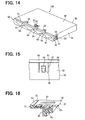
- the cutting sections 38 which configurate the case-side engaging parts, are not provided at the sidewalls 31 in a modification illustrated in FIG. 14 .
- the sidewalls 31 may have the case-side fixing parts and the engaging parts.
- the fixing holes 36 and the fixing projection 54 have the approximately rectangular plane shapes.
- the fixing holes 36 and the fixing projections 54 may have other shape as long as each of the fixing projections 54 can engage with corresponding one of the fixing holes 36.
- the fixing holes 36 and the fixing projections 54 may have approximately trapezoid plane shapes each having a width decreasing toward the rear wall side.
- narrower portions of the fixing projections 54 reach broader portions of the fixing holes 36 before the broader portions of the fixing projections 54 reach.
- the alignments are corrected by engaging the fixing projections 54 with the fixing holes 36.
- the shape of the spring grooves 37 is not limited to the approximately U-shape.
- two spring grooves 37 each having a linear shape extending from the open edge 35 toward the rear wall side may be arranged on opposite sides of the fixing holes 36.
- the case 30 have the fixing holes 36 and the housing 51 have the fixing projections 54, as an example.
- the fixing hole 60 may be a blind hole.
- the case 30 have the cutting section 38 and the housing 51 have the engaging projections 55, as an example.
- the engaging projection 44 has a base part 44a and a taper part 44b. The base part 44a is located between the inner surface 32c and a predetermined distance from the inner surface 32c and has a substantially constant width.
- the taper part 44b is located on the downside of the base part 44a and a width of the taper part 44b increases toward the downside.
- the edge portion 62 of the engaging groove 61 has a base part 62a and a taper part 62b.
- the base part 62a is located between the flat surface 51a of the housing 51 and a predetermined distance from the flat surface 51 a.
- the base part 62a corresponds to the base part 44a and has a substantially constant width.
- the taper part 62b is located on the downside of the base part 44a and a width of the taper part 62b increases toward the downside.
- the taper part 44b of the case 30 engages with the taper part 62b of the housing 51.
- Each of the case-side engaging parts and the housing-side engaging parts may also have an approximately trapezoid plate shape having a width decreasing toward the rear wall side.
- the positioning of the case 30 and the housing 51 in the longitudinal direction of the housing 51 can be improved.
- FIG. 18, FIG. 19A, and FIG. 19B An electronic control device 100 according to a second embodiment of the invention will be described with reference to FIG. 18, FIG. 19A, and FIG. 19B .
- the present electronic control device 100 has many portions in common with the electronic control device 100 according to the first embodiment, a description of the common portions will be omitted and different portions will be mainly described.
- Components of the present electronic control device 100 have the same reference numbers with similar components of the electronic control device 100 according to the first embodiment.
- each of the upper wall 32 and the lower wall 33 has the cutting section 38, which configurates the case-side engaging part, at the middle portion in the direction approximately perpendicular to the inserting direction of the printed circuit board 10.
- each of the upper wall 32 and the lower wall 33 has two fixing holes 36, which configurate the case-side fixing parts.
- the two fixing holes 36 are provided to be line symmetry with respect to the cutting section 38.
- the spring grooves 37 are provided in the vicinity of respective one of the fixing holes 36.
- the housing 51 has the fixing projections 54 and the engaging projections 55 so that each of the fixing projections 54 engages with corresponding one of the fixing holes 36 and each of the engaging projections 55 engage with corresponding one of the cutting sections 38.
- the housing-side fixing parts configured by the fixing projections 54 and the engaging parts configured by the engaging projections 55 are located on respective lines extended from the separating walls 59.
- each of the case-side engaging parts is located between two case-side fixing parts. That is, each of the upper wall 32 and the lower wall 33 has a plurality of case-side fixing parts.
- the case 30 is fixed to the connector 50 with a high degree of certainty even if the electronic control device 100 is applied with a stress in the inserting direction of the printed circuit board 10.
- a gouge in the longitudinal direction of the housing 51 is restricted.
- each of the cutting sections 38 has an approximately trapezoid plane shape that has a width decreasing toward the rear wall side.
- Each of the engaging projections 55 also has an approximately trapezoid plane shape corresponding to the cutting sections 38.
- the positioning of the case 30 and the housing 51 in the longitudinal direction of the housing 51 can be improved.
- a clearance between each of the engaging projections 55 and the edge portion 39 of corresponding one of the cutting sections 38 is smaller than a clearance between each of the fixing projections 54 and corresponding one of the fixing holes 36.
- the positioning of the case 30 and the housing 51 at the middle portion of the case 30 can be improved.
- a gouge that may be generated between the housing 51 and the case 30 can be reduced.
- FIG. 20 An electronic control device 100 according to a third embodiment of the invention will be described with reference to FIG. 20-FIG. 23 .
- the case 30 is illustrated in cross section and the printed circuit board 10 is not illustrated as a matter of convenience.
- the present electronic control device 100 has many portions in common with the electronic control device 100 according to the first embodiment, a description of the common portions will be omitted and different portions will be mainly described.
- Components of the present electronic control device 100 have the same reference numbers with similar components of the electronic control device 100 according to the first embodiment.
- the housing 51 has a lifting projection 63 on the flat surface 51a.
- the lifting projection 63 is located on an opposite side of one of the engaging projections 55 from one of the fixing projections 54.
- a protruding height of the lifting projection 63 from the flat surface 51a is less than the protruding height of the engaging projection 55.
- Other components in the present electronic control device 100 are similar to those in the electronic control device 100 according to the first embodiment.
- the lifting projection 63 lifts a portion of the case 30 located over the lifting projection 63 from the housing 51.
- the one engaging projection 55 can engage with the edge portion 39 of corresponding one of the cutting sections 38 more firmly at an outer surface side of the case 30.
- the lifting projection 63 can restrict a rattle between the case 30 and the connector 50 due to the clearance.
- a stress generated at a time when the connector 50 is fitted with the external connector can be effectively released from the housing 51 to the case 30 via the lifting projection 63. Because the lifting projection 63 is located on the opposite side of the one engaging projection 55 from the one fixing projection 54, the one fixing projection 54 can engage with corresponding one of the fixing holes 36 with a high degree of certainty even if the case 30 is lifted by the lifting projection 63.
- a stress may concentrate at corner portions 64 of the housing 51.
- corner portions 64 are rounded as illustrated in FIG. 20 .
- the stress concentration can be reduced.
- a thickness of each of corner portions 45 of the case 30 that correspond to the corner portions 64 of the housing 51 may be larger than other portion of the case 30.
- a rear end 63a of the lifting projection 63 is farther away from the rear wall 31a of the case 30 than the flat end 55c of the engaging projection 55, as illustrated in FIG. 22 .
- the lifting projection 63 comes into contact with the case 30 after the engaging projection 55 engages with the edge portion 39 of the cutting section 38.
- the engaging projection 55 can be engaged with the edge portion 39 of the cutting section 38 with certainty.
- a thickness of the edge portion 39 of each of the cutting section 38 may increase toward the rear wall side and a thickness of each of the engaging projection 55 may decrease toward the rear wall side corresponding to the edge portion 39 of corresponding one of the cutting sections 38.
- each of the engaging projection 55 can engage with the edge portion 39 of corresponding one of the cutting sections 38 with certainty even if the housing 51 is slightly separated from the case 30 at a time when the printed circuit board 10 is inserted into the case 30.
- the engagements of the case-side fixing parts and the housing-side fixing parts can be effectively restricted from being released.
- the lifting projection 63 may be provided in the electronic control device 100 according to the first embodiment or the modifications of the first embodiment.
- the case 30 may also have the lifting projection 63.
- the shape of engage projections 55 and the shape of the cutting sections 38 according to the present embodiment may also applied to the electronic control device 100 according to the first embodiment, the modifications of the first embodiment, or the second embodiment.
- the case 30 has the fixing holes 36 and the cutting sections 38 and the housing 51 has the fixing projections 54 and the engaging projections 55, as an example.
- the case 30 may have the fixing holes 36 and the engaging projections 44 and the housing 51 may have the fixing projections 54 and the engaging grooves 61. That is, the case 30 has one of a fixing hole and a fixing projection and one of an engaging projection and an engaged section (e.g., cutting section or engaging groove).
- the housing 51 has the other one of the fixing hole and the fixing projection and the other one of the engaging projection and the engaged section.
- each of the upper wall 32 and the lower wall 33 has the case-side fixing part and case-side engaging part.
- a wall where the case-side fixing part and the case-side engaging part are provided is not limited to the upper wall 32 and the lower wall 33.
- only the sidewalls 31 may have the case-side fixing part and the case-side engaging part.
- only one of the upper wall 32 and the lower wall 33 may have the case-side fixing part and the case-side engaging part.
- one wall has one case-side fixing part and two case-side engaging parts.
- one wall has two case-side fixing parts and one case-side engaging part.
- the number of the case-side fixing part and the case-side engaging part provided on one wall is not limited to the above-described example.
- one wall may have one case-side fixing part and one case-side engaging part.
- one wall may have a plurality of case-side fixing parts and a plurality of case-side engaging parts.
- the terminals 52 of the connector 50 have the surface mounting structure.
- the shapes of the terminals 52 are not limited to the above-described example.
- the terminals 52 may also have an insertion mounting structure or the terminals 52 may also have the surface mounting structure and the insertion mounting structure.
- the terminals 52 include the first terminals 52a, the second terminals 52b, and the third terminals 52c, as an example.
- the kind of the terminals 52 is not limited to the above-described example.
- the terminals 52 may have only the first terminals 52a and the second terminals 52b.
- the number, the type, and the arrangement of the terminal block are not limited to the above-described example.
- the second terminals 52b arranged at both longitudinal end portions of the connector 50 in FIG. 9 may be arranged above the first terminals 52a, i.e., in a fifth row in each of the terminal blocks 57 and 58.
- the number of row and the arrangement of the terminals 52 in the housing 51 are not limited to the above-described example.
- the electronic control device 100 is described as an example of an electronic device.
- the electronic control device may also be other device as long as the device includes the printed circuit board 10, the connector 50 mounted on the printed circuit board 10, and the case 30 housing the printed circuit board 10 therein and the opening portion 34 provided on one side of the case 30 is covered with the housing 51 of the connector 50.
- the spring grooves 37 are provided in the vicinity of the fixing holes 36 so that the portions of the case 30 located between the spring grooves 37 and the fixing holes 36 become the spring sections having the spring function.
- the fixing projections 54 may be configured to be spring sections having the spring function.
- the rear wall 31a of the case 30 has the holding groove 41.
- the shape and the position of the holding groove 41 are not limited to the above-described example.
- the shape and the position of the guide grooves 42 are not limited to the above-described example.
- the electronic control device 100 may not have the holding groove 41.
- each of the holding groove 41 and the guide grooves 42 may have a discontinuous shape.
- the protruding portion 53 has the ring shape so as to come into contact with the whole circumference of the case 30.
- the protruding portion 53 communicates with the engaging projections 55.
- the protruding portion 53 may also be away from the engaging projections 55 or the protruding portion 53 may also have a discontinuous shape.
- the fixing parts and the engaging parts are configured so that the engaging projections 55 engage with the edge portions 39 of the cutting sections 38 (i.e., the engage parts engage with each other) before the fixing projections 54 engages with the fixing holes 36 (i.e., the fixing parts engage with each other).
- the fixing parts may engage with each other before the engaging parts engage with each other.
- each of the upper wall 32 and the lower wall 33 is approximately flat.
- one of the upper wall 32 and the lower wall 33 may have a step portion.
- the upper wall 32 may have a step portion, and a front section of the upper wall 32 located on a front side of the step portion and adjacent to the opening portion 34 may be higher than a rear section of the upper wall 32 located on a rear side of the step portion, as illustrated in FIG. 24 .
- the rear wall 31a is integrally formed with the upper wall 32, the lower wall 33, and the two sidewalls 31 adjacent to the opening portion 34.
- the rear wall 31a may be formed separately from the upper wall 32, the lower wall 33, and the two sidewalls 31 adjacent to the opening portion 34.
- the printed circuit board 10 may be inserted into a case formed of the upper wall 32, the lower wall 33, and the two sidewalls 31 and having an approximately rectangular tubular shape, as illustrated in FIG. 25 , and then the rear wall 31a may be fixed to the case so that the holding groove 41 of the rear wall 31 is fitted with the rear end of the printed circuit board 10.
Landscapes
- Engineering & Computer Science (AREA)
- Microelectronics & Electronic Packaging (AREA)
- Casings For Electric Apparatus (AREA)
- Coupling Device And Connection With Printed Circuit (AREA)
- Connector Housings Or Holding Contact Members (AREA)
- Mounting Of Printed Circuit Boards And The Like (AREA)
Applications Claiming Priority (1)
| Application Number | Priority Date | Filing Date | Title |
|---|---|---|---|
| JP2007241481A JP4428430B2 (ja) | 2007-09-18 | 2007-09-18 | 電子装置 |
Publications (3)
| Publication Number | Publication Date |
|---|---|
| EP2040525A2 true EP2040525A2 (de) | 2009-03-25 |
| EP2040525A3 EP2040525A3 (de) | 2010-06-16 |
| EP2040525B1 EP2040525B1 (de) | 2012-09-19 |
Family
ID=40090242
Family Applications (1)
| Application Number | Title | Priority Date | Filing Date |
|---|---|---|---|
| EP08014452A Not-in-force EP2040525B1 (de) | 2007-09-18 | 2008-08-13 | Elektronische Vorrichtung mit Leiterplatte, Steckverbinder und Gehäuse |
Country Status (3)
| Country | Link |
|---|---|
| US (1) | US7686623B2 (de) |
| EP (1) | EP2040525B1 (de) |
| JP (1) | JP4428430B2 (de) |
Cited By (1)
| Publication number | Priority date | Publication date | Assignee | Title |
|---|---|---|---|---|
| CN112072351A (zh) * | 2019-06-10 | 2020-12-11 | 矢崎总业株式会社 | 电子部件单元 |
Families Citing this family (13)
| Publication number | Priority date | Publication date | Assignee | Title |
|---|---|---|---|---|
| JP2011119332A (ja) * | 2009-12-01 | 2011-06-16 | Autonetworks Technologies Ltd | 電子ユニット構成用モジュール及び電子ユニット |
| JP5605837B2 (ja) * | 2010-10-19 | 2014-10-15 | 株式会社ケーヒン | 電子制御装置 |
| JP2016504771A (ja) * | 2012-12-20 | 2016-02-12 | マグナ クロージャーズ インコーポレイテッド | コントローラエンクロージャアセンブリ |
| JP5543637B1 (ja) * | 2013-05-30 | 2014-07-09 | 株式会社フジクラ | コネクタ |
| TWI511637B (zh) * | 2013-09-04 | 2015-12-01 | Inventec Corp | 電子裝置 |
| JP6024680B2 (ja) * | 2014-02-05 | 2016-11-16 | 三菱電機株式会社 | コネクタ支持構造 |
| JP2016091738A (ja) * | 2014-10-31 | 2016-05-23 | パナソニックIpマネジメント株式会社 | 回路ユニット、及び、照明器具 |
| US9967993B1 (en) | 2016-11-07 | 2018-05-08 | Phoenix Contact Development and Manufacturing, Inc. | Printed circuit board enclosure assembly |
| JP2019067685A (ja) * | 2017-10-04 | 2019-04-25 | 矢崎総業株式会社 | 基板用コネクタ |
| JP2019145579A (ja) * | 2018-02-16 | 2019-08-29 | 日本精機株式会社 | 表示装置及びコネクタ付回路基板の保持構造 |
| JP2020023295A (ja) * | 2018-08-08 | 2020-02-13 | 日本電産モビリティ株式会社 | 水没検知装置、車両制御装置および車両 |
| JP7302424B2 (ja) * | 2019-10-11 | 2023-07-04 | 株式会社オートネットワーク技術研究所 | 電子ユニット |
| JP7302485B2 (ja) * | 2020-01-10 | 2023-07-04 | 株式会社デンソー | 電力分配装置 |
Citations (2)
| Publication number | Priority date | Publication date | Assignee | Title |
|---|---|---|---|---|
| JP2005160207A (ja) | 2003-11-26 | 2005-06-16 | Yazaki Corp | 電子ユニット |
| JP3769460B2 (ja) | 2000-10-25 | 2006-04-26 | 三菱電機株式会社 | 車載電子制御装置の筐体 |
Family Cites Families (8)
| Publication number | Priority date | Publication date | Assignee | Title |
|---|---|---|---|---|
| DE3310477A1 (de) * | 1982-07-17 | 1984-01-19 | Robert Bosch Gmbh, 7000 Stuttgart | Elektrisches geraet, insbesondere schalt- und steuergeraet fuer kraftfahrzeuge |
| JPH0341797A (ja) | 1989-07-07 | 1991-02-22 | Maspro Denkoh Corp | 電子機器用ケース |
| JPH0785931A (ja) * | 1993-09-17 | 1995-03-31 | Kel Corp | 電気コネクタ |
| JP3013756B2 (ja) * | 1995-05-31 | 2000-02-28 | 住友電装株式会社 | 基板用コネクタ |
| JP3745670B2 (ja) | 2001-10-23 | 2006-02-15 | 株式会社ケーヒン | 電子回路基板の収容ケース |
| JP2005101088A (ja) | 2003-09-22 | 2005-04-14 | Aisin Seiki Co Ltd | 固定部材 |
| JP4754287B2 (ja) * | 2005-07-15 | 2011-08-24 | 矢崎総業株式会社 | オンボードコネクタ |
| US7677905B2 (en) | 2006-12-13 | 2010-03-16 | Denso Corporation | Electronic device and manufacturing method of the same |
-
2007
- 2007-09-18 JP JP2007241481A patent/JP4428430B2/ja not_active Expired - Fee Related
-
2008
- 2008-08-12 US US12/222,556 patent/US7686623B2/en not_active Expired - Fee Related
- 2008-08-13 EP EP08014452A patent/EP2040525B1/de not_active Not-in-force
Patent Citations (2)
| Publication number | Priority date | Publication date | Assignee | Title |
|---|---|---|---|---|
| JP3769460B2 (ja) | 2000-10-25 | 2006-04-26 | 三菱電機株式会社 | 車載電子制御装置の筐体 |
| JP2005160207A (ja) | 2003-11-26 | 2005-06-16 | Yazaki Corp | 電子ユニット |
Cited By (2)
| Publication number | Priority date | Publication date | Assignee | Title |
|---|---|---|---|---|
| CN112072351A (zh) * | 2019-06-10 | 2020-12-11 | 矢崎总业株式会社 | 电子部件单元 |
| CN112072351B (zh) * | 2019-06-10 | 2022-03-01 | 矢崎总业株式会社 | 电子部件单元 |
Also Published As
| Publication number | Publication date |
|---|---|
| EP2040525A3 (de) | 2010-06-16 |
| EP2040525B1 (de) | 2012-09-19 |
| US20090075501A1 (en) | 2009-03-19 |
| JP4428430B2 (ja) | 2010-03-10 |
| JP2009076213A (ja) | 2009-04-09 |
| US7686623B2 (en) | 2010-03-30 |
Similar Documents
| Publication | Publication Date | Title |
|---|---|---|
| EP2040525B1 (de) | Elektronische Vorrichtung mit Leiterplatte, Steckverbinder und Gehäuse | |
| EP2034811B1 (de) | Elektronische Vorrichtung mit Leiterplatte, Steckverbinder und Gehäuse | |
| CN101316030B (zh) | 电接线盒 | |
| EP2034809B1 (de) | Elektronische Vorrichtung mit Leiterplatte und auf der Leiterplatte montiertes elektronisches Element | |
| JP4692604B2 (ja) | 車両室内用光源装置 | |
| US10680377B2 (en) | Housing structure of printed circuit board with connector | |
| JP6074289B2 (ja) | 雌コネクタ及びカードエッジコネクタ | |
| JP4041423B2 (ja) | 電気接続箱の防水構造 | |
| JP4030954B2 (ja) | レセプタクル電気コネクタ | |
| CN112072351B (zh) | 电子部件单元 | |
| CN109922616B (zh) | 电子控制装置 | |
| CN110364870A (zh) | 电子部件模块,电连接盒,以及线束 | |
| JP3108072U (ja) | エアバッグ制御装置用メタル・ハウジング | |
| JP5108710B2 (ja) | 電気コネクタ | |
| US7682183B2 (en) | Electric junction box | |
| CN112449543A (zh) | 基板壳体及电连接箱 | |
| JP2017175069A (ja) | 電子制御装置 | |
| JP3961937B2 (ja) | 基板用電気コネクタ | |
| JP5633197B2 (ja) | 電気接続箱 | |
| JP2006005209A (ja) | 電子回路基板とコネクタの固定構造 | |
| JP3761425B2 (ja) | コネクタ構造 | |
| JP7686348B2 (ja) | コンデンサ | |
| JP5630103B2 (ja) | 電気接続箱 | |
| KR20200069501A (ko) | 안테나를 구비한 전자 제어 장치 | |
| JP2002280100A (ja) | 回路基板用電気コネクタ |
Legal Events
| Date | Code | Title | Description |
|---|---|---|---|
| PUAI | Public reference made under article 153(3) epc to a published international application that has entered the european phase |
Free format text: ORIGINAL CODE: 0009012 |
|
| AK | Designated contracting states |
Kind code of ref document: A2 Designated state(s): AT BE BG CH CY CZ DE DK EE ES FI FR GB GR HR HU IE IS IT LI LT LU LV MC MT NL NO PL PT RO SE SI SK TR |
|
| AX | Request for extension of the european patent |
Extension state: AL BA MK RS |
|
| PUAL | Search report despatched |
Free format text: ORIGINAL CODE: 0009013 |
|
| AK | Designated contracting states |
Kind code of ref document: A3 Designated state(s): AT BE BG CH CY CZ DE DK EE ES FI FR GB GR HR HU IE IS IT LI LT LU LV MC MT NL NO PL PT RO SE SI SK TR |
|
| AX | Request for extension of the european patent |
Extension state: AL BA MK RS |
|
| 17P | Request for examination filed |
Effective date: 20101021 |
|
| AKX | Designation fees paid |
Designated state(s): DE FR |
|
| GRAP | Despatch of communication of intention to grant a patent |
Free format text: ORIGINAL CODE: EPIDOSNIGR1 |
|
| GRAS | Grant fee paid |
Free format text: ORIGINAL CODE: EPIDOSNIGR3 |
|
| GRAA | (expected) grant |
Free format text: ORIGINAL CODE: 0009210 |
|
| AK | Designated contracting states |
Kind code of ref document: B1 Designated state(s): DE FR |
|
| REG | Reference to a national code |
Ref country code: DE Ref legal event code: R096 Ref document number: 602008018824 Country of ref document: DE Effective date: 20121108 |
|
| PLBE | No opposition filed within time limit |
Free format text: ORIGINAL CODE: 0009261 |
|
| STAA | Information on the status of an ep patent application or granted ep patent |
Free format text: STATUS: NO OPPOSITION FILED WITHIN TIME LIMIT |
|
| 26N | No opposition filed |
Effective date: 20130620 |
|
| REG | Reference to a national code |
Ref country code: DE Ref legal event code: R084 Ref document number: 602008018824 Country of ref document: DE |
|
| REG | Reference to a national code |
Ref country code: DE Ref legal event code: R097 Ref document number: 602008018824 Country of ref document: DE Effective date: 20130620 |
|
| REG | Reference to a national code |
Ref country code: DE Ref legal event code: R084 Ref document number: 602008018824 Country of ref document: DE Effective date: 20130917 |
|
| REG | Reference to a national code |
Ref country code: FR Ref legal event code: PLFP Year of fee payment: 8 |
|
| PGFP | Annual fee paid to national office [announced via postgrant information from national office to epo] |
Ref country code: FR Payment date: 20150626 Year of fee payment: 8 |
|
| REG | Reference to a national code |
Ref country code: FR Ref legal event code: ST Effective date: 20170428 |
|
| PG25 | Lapsed in a contracting state [announced via postgrant information from national office to epo] |
Ref country code: FR Free format text: LAPSE BECAUSE OF NON-PAYMENT OF DUE FEES Effective date: 20160831 |
|
| PGFP | Annual fee paid to national office [announced via postgrant information from national office to epo] |
Ref country code: DE Payment date: 20220620 Year of fee payment: 15 |
|
| REG | Reference to a national code |
Ref country code: DE Ref legal event code: R119 Ref document number: 602008018824 Country of ref document: DE |
|
| PG25 | Lapsed in a contracting state [announced via postgrant information from national office to epo] |
Ref country code: DE Free format text: LAPSE BECAUSE OF NON-PAYMENT OF DUE FEES Effective date: 20240301 |