EP2045371A2 - Verfahren und Vorrichtung zur Herstellung eines Einkristallblock-Halbleiters mit sehr wenigen Fehlern - Google Patents
Verfahren und Vorrichtung zur Herstellung eines Einkristallblock-Halbleiters mit sehr wenigen Fehlern Download PDFInfo
- Publication number
- EP2045371A2 EP2045371A2 EP08017323A EP08017323A EP2045371A2 EP 2045371 A2 EP2045371 A2 EP 2045371A2 EP 08017323 A EP08017323 A EP 08017323A EP 08017323 A EP08017323 A EP 08017323A EP 2045371 A2 EP2045371 A2 EP 2045371A2
- Authority
- EP
- European Patent Office
- Prior art keywords
- single crystalline
- crystalline ingot
- melt
- semiconductor
- manufacturing
- Prior art date
- Legal status (The legal status is an assumption and is not a legal conclusion. Google has not performed a legal analysis and makes no representation as to the accuracy of the status listed.)
- Granted
Links
Images


Classifications
-
- C—CHEMISTRY; METALLURGY
- C30—CRYSTAL GROWTH
- C30B—SINGLE-CRYSTAL GROWTH; UNIDIRECTIONAL SOLIDIFICATION OF EUTECTIC MATERIAL OR UNIDIRECTIONAL DEMIXING OF EUTECTOID MATERIAL; REFINING BY ZONE-MELTING OF MATERIAL; PRODUCTION OF A HOMOGENEOUS POLYCRYSTALLINE MATERIAL WITH DEFINED STRUCTURE; SINGLE CRYSTALS OR HOMOGENEOUS POLYCRYSTALLINE MATERIAL WITH DEFINED STRUCTURE; AFTER-TREATMENT OF SINGLE CRYSTALS OR A HOMOGENEOUS POLYCRYSTALLINE MATERIAL WITH DEFINED STRUCTURE; APPARATUS THEREFOR
- C30B15/00—Single-crystal growth by pulling from a melt, e.g. Czochralski method
- C30B15/20—Controlling or regulating
-
- C—CHEMISTRY; METALLURGY
- C30—CRYSTAL GROWTH
- C30B—SINGLE-CRYSTAL GROWTH; UNIDIRECTIONAL SOLIDIFICATION OF EUTECTIC MATERIAL OR UNIDIRECTIONAL DEMIXING OF EUTECTOID MATERIAL; REFINING BY ZONE-MELTING OF MATERIAL; PRODUCTION OF A HOMOGENEOUS POLYCRYSTALLINE MATERIAL WITH DEFINED STRUCTURE; SINGLE CRYSTALS OR HOMOGENEOUS POLYCRYSTALLINE MATERIAL WITH DEFINED STRUCTURE; AFTER-TREATMENT OF SINGLE CRYSTALS OR A HOMOGENEOUS POLYCRYSTALLINE MATERIAL WITH DEFINED STRUCTURE; APPARATUS THEREFOR
- C30B15/00—Single-crystal growth by pulling from a melt, e.g. Czochralski method
- C30B15/14—Heating of the melt or the crystallised materials
-
- C—CHEMISTRY; METALLURGY
- C30—CRYSTAL GROWTH
- C30B—SINGLE-CRYSTAL GROWTH; UNIDIRECTIONAL SOLIDIFICATION OF EUTECTIC MATERIAL OR UNIDIRECTIONAL DEMIXING OF EUTECTOID MATERIAL; REFINING BY ZONE-MELTING OF MATERIAL; PRODUCTION OF A HOMOGENEOUS POLYCRYSTALLINE MATERIAL WITH DEFINED STRUCTURE; SINGLE CRYSTALS OR HOMOGENEOUS POLYCRYSTALLINE MATERIAL WITH DEFINED STRUCTURE; AFTER-TREATMENT OF SINGLE CRYSTALS OR A HOMOGENEOUS POLYCRYSTALLINE MATERIAL WITH DEFINED STRUCTURE; APPARATUS THEREFOR
- C30B15/00—Single-crystal growth by pulling from a melt, e.g. Czochralski method
- C30B15/20—Controlling or regulating
- C30B15/203—Controlling or regulating the relationship of pull rate (v) to axial thermal gradient (G)
-
- C—CHEMISTRY; METALLURGY
- C30—CRYSTAL GROWTH
- C30B—SINGLE-CRYSTAL GROWTH; UNIDIRECTIONAL SOLIDIFICATION OF EUTECTIC MATERIAL OR UNIDIRECTIONAL DEMIXING OF EUTECTOID MATERIAL; REFINING BY ZONE-MELTING OF MATERIAL; PRODUCTION OF A HOMOGENEOUS POLYCRYSTALLINE MATERIAL WITH DEFINED STRUCTURE; SINGLE CRYSTALS OR HOMOGENEOUS POLYCRYSTALLINE MATERIAL WITH DEFINED STRUCTURE; AFTER-TREATMENT OF SINGLE CRYSTALS OR A HOMOGENEOUS POLYCRYSTALLINE MATERIAL WITH DEFINED STRUCTURE; APPARATUS THEREFOR
- C30B15/00—Single-crystal growth by pulling from a melt, e.g. Czochralski method
- C30B15/20—Controlling or regulating
- C30B15/206—Controlling or regulating the thermal history of growing the ingot
-
- C—CHEMISTRY; METALLURGY
- C30—CRYSTAL GROWTH
- C30B—SINGLE-CRYSTAL GROWTH; UNIDIRECTIONAL SOLIDIFICATION OF EUTECTIC MATERIAL OR UNIDIRECTIONAL DEMIXING OF EUTECTOID MATERIAL; REFINING BY ZONE-MELTING OF MATERIAL; PRODUCTION OF A HOMOGENEOUS POLYCRYSTALLINE MATERIAL WITH DEFINED STRUCTURE; SINGLE CRYSTALS OR HOMOGENEOUS POLYCRYSTALLINE MATERIAL WITH DEFINED STRUCTURE; AFTER-TREATMENT OF SINGLE CRYSTALS OR A HOMOGENEOUS POLYCRYSTALLINE MATERIAL WITH DEFINED STRUCTURE; APPARATUS THEREFOR
- C30B29/00—Single crystals or homogeneous polycrystalline material with defined structure characterised by the material or by their shape
- C30B29/02—Elements
- C30B29/06—Silicon
-
- H—ELECTRICITY
- H10—SEMICONDUCTOR DEVICES; ELECTRIC SOLID-STATE DEVICES NOT OTHERWISE PROVIDED FOR
- H10P—GENERIC PROCESSES OR APPARATUS FOR THE MANUFACTURE OR TREATMENT OF DEVICES COVERED BY CLASS H10
- H10P14/00—Formation of materials, e.g. in the shape of layers or pillars
- H10P14/20—Formation of materials, e.g. in the shape of layers or pillars of semiconductor materials
-
- Y—GENERAL TAGGING OF NEW TECHNOLOGICAL DEVELOPMENTS; GENERAL TAGGING OF CROSS-SECTIONAL TECHNOLOGIES SPANNING OVER SEVERAL SECTIONS OF THE IPC; TECHNICAL SUBJECTS COVERED BY FORMER USPC CROSS-REFERENCE ART COLLECTIONS [XRACs] AND DIGESTS
- Y10—TECHNICAL SUBJECTS COVERED BY FORMER USPC
- Y10T—TECHNICAL SUBJECTS COVERED BY FORMER US CLASSIFICATION
- Y10T117/00—Single-crystal, oriented-crystal, and epitaxy growth processes; non-coating apparatus therefor
- Y10T117/10—Apparatus
- Y10T117/1024—Apparatus for crystallization from liquid or supercritical state
- Y10T117/1032—Seed pulling
- Y10T117/1068—Seed pulling including heating or cooling details [e.g., shield configuration]
Definitions
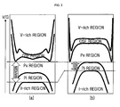
- a process margin in the manufacture of a defect-free single crystalline ingot is influenced by a vertical temperature gradient of a radial direction, and thus invariably, the temperature gradient should be large and uniform in a radial direction.
- a conventional technique for manufacturing a single crystalline ingot of 12 inch diameter and at least 300kg or 400kg weight exhibits a narrow process margin due to reduction in a G value of an edge portion, and when manufacturing an Si wafer, causes a DSOD (Direct Surface Oxide Defect) defect (See FIG. 2(b) ) in the shape of a ring at a peripheral portion of the wafer, thereby failing to manufacture a defect-free wafer, in which a defect-free margin is uniformly maintained in a radial direction.
- DSOD Direct Surface Oxide Defect
- a charge size is small, for example a single crystalline ingot is grown to 400kg or 300kg or less, a latent heat of solidification is relatively small, and thus a pulling speed should be controlled uniformly from an initial stage of growth to the last stage to maintain a margin uniformly, which may reduce productivity.
- FIG. 3 shows that as a G value of an edge portion of a single crystalline ingot reduces at the last stage of a single crystalline ingot growth process, a defect-free margin at the last stage remarkably reduces in comparison with a defect-free margin at an initial stage.
- this is mainly resulted from a change of latent heat due to change in a residual melt, and reduction in a G value of an edge portion caused by change in the shape of a melt flow and heat transmission due to a hot zone.
- the present invention is designed to solve the problems of the prior arts. Therefore, it is an object of the present invention to provide a method and apparatus for manufacturing an ultra low defect semiconductor single crystalline ingot that controls a cooling efficiency of a single crystalline ingot according to length of the single crystalline ingot to uniformly maintain or increase a defect-free margin throughout a process and improve a pulling speed.
- the present invention provides a method for manufacturing an ultra low defect semiconductor single crystalline ingot that uses a Czochralski process for growing a semiconductor single crystalline ingot through a solid-liquid interface by dipping a seed into a semiconductor melt received in a quartz crucible and slowly pulling up the seed while rotating the seed, wherein a defect-free margin is controlled by increasing or decreasing a heat space on a surface of the semiconductor melt according to change in length of the single crystalline ingot as progress of the single crystalline ingot growth process.
- the heat space may be increased or decreased by differentially changing a melt gap between a bottom of a heat shield structure spaced away from an outer periphery of the single crystalline ingot and the surface of the semiconductor melt according to length of the single crystalline ingot.
- the melt gap is controlled in the range of 25mm or less.
- an apparatus for manufacturing an ultra low defect semiconductor single crystalline ingot that performs a Czochralski process for growing a semiconductor single crystalline ingot through a solid-liquid interface by dipping a seed into a semiconductor melt received in a quartz crucible and slowly pulling up the seed while rotating the seed, includes a heat space control unit for controlling a defect-free margin by increasing or decreasing a heat space on a surface of the semiconductor melt according to change in length of the single crystalline ingot as progress of the single crystalline ingot growth process.
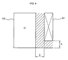
- FIG. 4 is a side view showing schematically a heat space on a silicon melt for description of a method for manufacturing an ultra low defect single crystalline ingot according to a preferred embodiment of the present invention.
- the present invention performs a Czochralksi process for growing a silicon single crystalline ingot 100 through a solid-liquid interface by dipping a seed into a silicon melt received in a quartz crucible and pulling up the seed while rotating the seed, and during crystalline ingot growth, controls a heat space (slanted lines) on a surface of a silicon melt or efficiency of the heat space to control a defect-free margin.
- the heat space is increased or decreased by changing a location of the heat shield structure 101 according to change in length of the silicon single crystalline ingot 100 as progress of a single crystalline ingot growth process.
- the heat space may be controlled by changing a gap, or a melt gap (A) between the surface of the silicon melt and the bottom of the heat shield structure 101, or an interval (B) between the outer periphery of the silicon single crystalline ingot 100 and the heat shield structure 101, or a combination thereof.
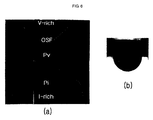
- the present invention changes a melt gap according to length of a single crystalline ingot during a single crystalline ingot growth process, so a temperature gradient in a radial direction is uniformly maintained from an initial stage of crystalline ingot growth (See FIG. 5(a) ) to an intermediate stage of crystalline ingot growth and thereafter (See FIG. 5(b) ).
- a defect-free margin can be maintained uniformly, and both of G values of a center portion and an edge portion are increased to improve a pulling speed.
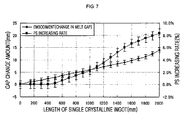
- FIG. 7 shows an actual experimental example, in which the heat space is reduced by decreasing a melt gap according to change in length of a growing single crystalline ingot for smooth heat radiation.
- a horizontal axis is a length of a single crystalline ingot changing according to crystalline ingot growth
- a left vertical axis is a change (reduction) amount of a melt gap
- a right vertical axis is an increasing rate of pulling speed (PS).
- PS pulling speed
- the PS increasing rate indicates the percentage of a degree of an improved PS value to a previous PS value.
- a pulling speed (V) of the single crystalline ingot is set to satisfy the following equation.
- V a + b * L + C * (a, b, c: constant, L: length of a single crystalline ingot, ⁇ Gap: a change amount of a melt gap)
- FIG. 8 is a graph showing an example of a change in a defect-free margin according to level of reduction of a heat space through reduction of a melt gap. It is found that as a melt gap is reduced to 12 to 14mm, a defect-free margin that was 0.01mm /min at an initial point, is increased up to 0.025mm/min or more, and thereafter is reduced. This shows that as reduction in a G value of an edge portion of a single crystalline ingot is improved according to level of a melt gap, a quality margin is improved, but in the case that the G value exceeds a critical value, the excessively increased G value of the edge portion causes a relative reduction of a G value of a center portion of the single crystalline ingot, which is opposite to the conventional phenomenon.
- a control pattern of the heat space can be variably changed depending on structure or shape of a heat shield structure. That is, for example, in the case that a space surround by the heat shield structure is relatively narrow, the heat space can be controlled by setting a level of change in a melt gap relatively small.
- a level of reduction of the melt gap is set to 25mm or less as shown in FIG. 7 .
- FIG. 9 is a view showing a main configuration of an apparatus for manufacturing a single crystalline ingot according to a preferred embodiment of the present invention.
- the quartz crucible rotating means 30 is installed below the crucible support 20, and rotates the crucible support 20 and the quartz crucible 10 and slowly moves up the quartz crucible 10 in order to uniformly maintain the height of a solid-liquid interface.
- the heating means 40 is spaced a predetermined distance away from a side wall of the crucible support 20 and heats the quartz crucible 10.
- the adiabatic means 50 is installed outside of the heating means 40 and prevents heat generated from the heating means 40 from emitting to the external environment.
- the single crystalline ingot pulling means 60 pulls a silicon single crystalline ingot 100 from the silicon melt (SM) received in the quartz crucible 10 by use of a seed rotating in a predetermined direction.
- the heat shield structure 101 is spaced a predetermined distance away from an outer periphery of the silicon single crystalline ingot 100 and shields heat emitted from the silicon single crystalline ingot 100.
- the inert gas supply means (not shown) supplies an inert gas (for example, Ar gas) to an upper surface of the silicon melt (SM) along the outer periphery of the silicon single crystalline ingot 100.
- the heat space control unit 200 controls a heat space on the silicon melt (SM).
- the heat space control unit 200 controls the heat space, for examples, increases or decreases the heat space according to change in length of the single crystalline ingot as progress of a single crystalline ingot growth process.
- the heat space may be controlled by changing a location of the heat shield structure, however the present invention is not limited in this regard.
- the heat space control unit 200 includes a predetermined drive tool and a controller for controlling the drive tool to increase or decrease the heat space by moving the heat shield structure 101.
- the present invention controls the heat space on the silicon melt to uniformly maintain a temperature gradient in a radial direction ranging from a center portion to an edge portion of the single crystalline ingot, thereby substantially sufficiently securing a defect-free margin from an initial stage of crystalline ingot growth to a last stage of crystalline ingot growth.
- the entire G value according to length of the single crystal increases to improve a pulling speed and consequently increase productivity, and to eliminate the need for change in design of the heat shield structure, thereby reducing the installation costs.
- the present invention can be advantageously applicable to, in particular, 12 inch defect-free silicon single crystalline ingot growth. That is, in the case of a 12 inch silicon single crystal manufactured with a large quantity charge of at least 300kg or 400kg, a crucible receiving a silicon melt and a heat shield structure surrounding the crucible are increased in size, and consequently an amount of heat accumulated in the heat shield structure is remarkably increased. Further, the convection of the silicon melt is suppressed by a strong electromagnetic field of at least 2000G or 3000G applied during the process, thereby suppressing heat emission, so that a G value of the edge portion of the single crystalline ingot is lowered.
- the present invention can solve the above-mentioned problems by decreasing the heat space.
Landscapes
- Chemical & Material Sciences (AREA)
- Engineering & Computer Science (AREA)
- Crystallography & Structural Chemistry (AREA)
- Materials Engineering (AREA)
- Metallurgy (AREA)
- Organic Chemistry (AREA)
- Crystals, And After-Treatments Of Crystals (AREA)
Applications Claiming Priority (1)
| Application Number | Priority Date | Filing Date | Title |
|---|---|---|---|
| KR1020070099804A KR20090034534A (ko) | 2007-10-04 | 2007-10-04 | 극저결함 반도체 단결정의 제조방법 및 그 제조 장치 |
Publications (3)
| Publication Number | Publication Date |
|---|---|
| EP2045371A2 true EP2045371A2 (de) | 2009-04-08 |
| EP2045371A3 EP2045371A3 (de) | 2010-09-22 |
| EP2045371B1 EP2045371B1 (de) | 2013-04-10 |
Family
ID=40091340
Family Applications (1)
| Application Number | Title | Priority Date | Filing Date |
|---|---|---|---|
| EP08017323.0A Active EP2045371B1 (de) | 2007-10-04 | 2008-10-01 | Verfahren und Vorrichtung zur Herstellung eines Einkristallblock-Halbleiters mit sehr wenigen Fehlern |
Country Status (5)
| Country | Link |
|---|---|
| US (1) | US8574362B2 (de) |
| EP (1) | EP2045371B1 (de) |
| JP (1) | JP5415052B2 (de) |
| KR (1) | KR20090034534A (de) |
| CN (1) | CN101403137A (de) |
Families Citing this family (5)
| Publication number | Priority date | Publication date | Assignee | Title |
|---|---|---|---|---|
| JP4432458B2 (ja) * | 2003-10-30 | 2010-03-17 | 信越半導体株式会社 | 単結晶の製造方法 |
| JP6885286B2 (ja) * | 2017-09-28 | 2021-06-09 | 株式会社Sumco | シリコン単結晶の製造方法 |
| KR102037751B1 (ko) * | 2018-01-09 | 2019-10-29 | 에스케이실트론 주식회사 | 실리콘 웨이퍼 제조 방법 및 장치 |
| CN111926384B (zh) * | 2020-06-05 | 2022-06-17 | 徐州鑫晶半导体科技有限公司 | 单晶炉、确定该单晶炉在单晶硅生长过程中操作参数的方法以及制备单晶硅的方法 |
| CN115985798A (zh) * | 2022-12-05 | 2023-04-18 | 上海新昇半导体科技有限公司 | 一种单晶硅晶圆中缺陷类型的判定方法 |
Citations (5)
| Publication number | Priority date | Publication date | Assignee | Title |
|---|---|---|---|---|
| EP1347083A1 (de) | 2000-12-28 | 2003-09-24 | Shin-Etsu Handotai Co., Ltd | Sliziumeinkristallscheibe und herstellungsverfahren für siliziumeinkristall |
| JP2004137093A (ja) | 2002-10-16 | 2004-05-13 | Sumitomo Mitsubishi Silicon Corp | シリコン単結晶引上げ装置の不活性ガスの流速制御装置及びその流速制御方法 |
| JP2005015296A (ja) | 2003-06-27 | 2005-01-20 | Shin Etsu Handotai Co Ltd | 単結晶の製造方法及び単結晶 |
| US20060016387A1 (en) | 2002-11-14 | 2006-01-26 | Takashi Yokoyama | Silicon wafer, its manufacturing method, and its manufacturing apparatus |
| US20070151505A1 (en) | 2005-12-30 | 2007-07-05 | Siltron Inc. | Method for producing high quality silicon single crystal ingot and silicon single crystal wafer made thereby |
Family Cites Families (5)
| Publication number | Priority date | Publication date | Assignee | Title |
|---|---|---|---|---|
| JPS5913693A (ja) * | 1982-07-15 | 1984-01-24 | Toshiba Corp | 化合物半導体単結晶育成装置 |
| US6503594B2 (en) * | 1997-02-13 | 2003-01-07 | Samsung Electronics Co., Ltd. | Silicon wafers having controlled distribution of defects and slip |
| US6171391B1 (en) * | 1998-10-14 | 2001-01-09 | Memc Electronic Materials, Inc. | Method and system for controlling growth of a silicon crystal |
| JP2005015290A (ja) | 2003-06-27 | 2005-01-20 | Shin Etsu Handotai Co Ltd | 単結晶の製造方法及び単結晶 |
| JP2006069803A (ja) | 2004-08-31 | 2006-03-16 | Sumco Corp | シリコン単結晶引上げ装置の熱遮蔽部材 |
-
2007
- 2007-10-04 KR KR1020070099804A patent/KR20090034534A/ko not_active Ceased
-
2008
- 2008-10-01 JP JP2008256592A patent/JP5415052B2/ja active Active
- 2008-10-01 EP EP08017323.0A patent/EP2045371B1/de active Active
- 2008-10-02 US US12/244,283 patent/US8574362B2/en active Active
- 2008-10-06 CN CNA2008101682233A patent/CN101403137A/zh active Pending
Patent Citations (6)
| Publication number | Priority date | Publication date | Assignee | Title |
|---|---|---|---|---|
| EP1347083A1 (de) | 2000-12-28 | 2003-09-24 | Shin-Etsu Handotai Co., Ltd | Sliziumeinkristallscheibe und herstellungsverfahren für siliziumeinkristall |
| JP2004137093A (ja) | 2002-10-16 | 2004-05-13 | Sumitomo Mitsubishi Silicon Corp | シリコン単結晶引上げ装置の不活性ガスの流速制御装置及びその流速制御方法 |
| US20060016387A1 (en) | 2002-11-14 | 2006-01-26 | Takashi Yokoyama | Silicon wafer, its manufacturing method, and its manufacturing apparatus |
| JP2005015296A (ja) | 2003-06-27 | 2005-01-20 | Shin Etsu Handotai Co Ltd | 単結晶の製造方法及び単結晶 |
| EP1650332A1 (de) | 2003-06-27 | 2006-04-26 | Shin-Etsu Handotai Co., Ltd | Verfahren zur einkristallherstellung und einkristall |
| US20070151505A1 (en) | 2005-12-30 | 2007-07-05 | Siltron Inc. | Method for producing high quality silicon single crystal ingot and silicon single crystal wafer made thereby |
Also Published As
| Publication number | Publication date |
|---|---|
| EP2045371A3 (de) | 2010-09-22 |
| KR20090034534A (ko) | 2009-04-08 |
| EP2045371B1 (de) | 2013-04-10 |
| US8574362B2 (en) | 2013-11-05 |
| US20090090294A1 (en) | 2009-04-09 |
| JP2009091237A (ja) | 2009-04-30 |
| CN101403137A (zh) | 2009-04-08 |
| JP5415052B2 (ja) | 2014-02-12 |
Similar Documents
| Publication | Publication Date | Title |
|---|---|---|
| US7524371B2 (en) | Method for manufacturing defect-free silicon single crystal | |
| CN101400834B (zh) | 硅单晶提拉装置 | |
| US8574362B2 (en) | Method and apparatus for manufacturing an ultra low defect semiconductor single crystalline ingot | |
| US20060016387A1 (en) | Silicon wafer, its manufacturing method, and its manufacturing apparatus | |
| US8864906B2 (en) | Method for producing silicon wafer | |
| KR101028297B1 (ko) | 단결정의 산소 농도구배 제어방법 | |
| JP2010018446A (ja) | 単結晶の製造方法及び単結晶引上装置 | |
| EP3956499B1 (de) | Verfahren zur züchtung eines einkristallsiliciumblocks unter verwendung eines kontinuierlichen czochralski-verfahrens | |
| JP2009057270A (ja) | シリコン単結晶の引上方法 | |
| KR100331552B1 (ko) | 잉곳-용융물 경계의 중앙 및 가장자리에서의 온도구배의 조절에 의한 단결정 실리콘 잉곳의 제조를 위한 초크랄스키 풀러, 상기 초크랄스키 풀러용 열차단체 및 상기 초크랄스키 풀러의 개량방법. | |
| EP1614774A1 (de) | Einkristallherstellungsverfahren | |
| KR101218664B1 (ko) | 탄소가 도핑된 반도체 단결정 잉곳 및 그 제조 방법 | |
| US7427325B2 (en) | Method for producing high quality silicon single crystal ingot and silicon single crystal wafer made thereby | |
| JP2009274888A (ja) | シリコン単結晶製造方法及びシリコン単結晶ウェーハ | |
| JP2004161566A (ja) | シリコンウェーハの製造方法およびその製造装置およびシリコンウェーハ | |
| KR100800253B1 (ko) | 실리콘 단결정 제조방법 | |
| JP2020114802A (ja) | シリコン単結晶の製造方法 | |
| JP2009242237A (ja) | 単結晶インゴット製造装置及び方法 | |
| JP4758338B2 (ja) | 単結晶半導体の製造方法 | |
| JP2007284260A (ja) | シリコン単結晶の製造方法 | |
| KR101540567B1 (ko) | 단결정 잉곳, 이를 제조하는 방법 및 장치 | |
| KR100906281B1 (ko) | 실리콘 단결정 잉곳 성장장치의 열실드 구조물 및 이를 이용한 실리콘 단결정 잉곳 성장장치 | |
| JP6777739B2 (ja) | 単結晶インゴット成長装置 | |
| KR100690959B1 (ko) | 단결정 잉곳의 성장 장치 | |
| JP5150865B2 (ja) | シリコン単結晶インゴットの製造方法 |
Legal Events
| Date | Code | Title | Description |
|---|---|---|---|
| PUAI | Public reference made under article 153(3) epc to a published international application that has entered the european phase |
Free format text: ORIGINAL CODE: 0009012 |
|
| AK | Designated contracting states |
Kind code of ref document: A2 Designated state(s): AT BE BG CH CY CZ DE DK EE ES FI FR GB GR HR HU IE IS IT LI LT LU LV MC MT NL NO PL PT RO SE SI SK TR |
|
| AX | Request for extension of the european patent |
Extension state: AL BA MK RS |
|
| PUAL | Search report despatched |
Free format text: ORIGINAL CODE: 0009013 |
|
| AK | Designated contracting states |
Kind code of ref document: A3 Designated state(s): AT BE BG CH CY CZ DE DK EE ES FI FR GB GR HR HU IE IS IT LI LT LU LV MC MT NL NO PL PT RO SE SI SK TR |
|
| AX | Request for extension of the european patent |
Extension state: AL BA MK RS |
|
| 17P | Request for examination filed |
Effective date: 20110322 |
|
| AKX | Designation fees paid |
Designated state(s): DE FR IT |
|
| 17Q | First examination report despatched |
Effective date: 20120515 |
|
| GRAP | Despatch of communication of intention to grant a patent |
Free format text: ORIGINAL CODE: EPIDOSNIGR1 |
|
| RIN1 | Information on inventor provided before grant (corrected) |
Inventor name: HONG, YOUNG-HO Inventor name: LEE, HONG-WOO Inventor name: CHO, HYON-JONG Inventor name: LEE, SUNG-YOUNG Inventor name: SHIN, SEUNG-HO |
|
| GRAS | Grant fee paid |
Free format text: ORIGINAL CODE: EPIDOSNIGR3 |
|
| GRAA | (expected) grant |
Free format text: ORIGINAL CODE: 0009210 |
|
| AK | Designated contracting states |
Kind code of ref document: B1 Designated state(s): DE FR IT |
|
| REG | Reference to a national code |
Ref country code: DE Ref legal event code: R096 Ref document number: 602008023596 Country of ref document: DE Effective date: 20130606 |
|
| PLBE | No opposition filed within time limit |
Free format text: ORIGINAL CODE: 0009261 |
|
| STAA | Information on the status of an ep patent application or granted ep patent |
Free format text: STATUS: NO OPPOSITION FILED WITHIN TIME LIMIT |
|
| 26N | No opposition filed |
Effective date: 20140113 |
|
| REG | Reference to a national code |
Ref country code: DE Ref legal event code: R097 Ref document number: 602008023596 Country of ref document: DE Effective date: 20140113 |
|
| REG | Reference to a national code |
Ref country code: FR Ref legal event code: PLFP Year of fee payment: 8 |
|
| REG | Reference to a national code |
Ref country code: FR Ref legal event code: PLFP Year of fee payment: 9 |
|
| REG | Reference to a national code |
Ref country code: FR Ref legal event code: PLFP Year of fee payment: 10 |
|
| REG | Reference to a national code |
Ref country code: FR Ref legal event code: PLFP Year of fee payment: 11 |
|
| PGFP | Annual fee paid to national office [announced via postgrant information from national office to epo] |
Ref country code: FR Payment date: 20220920 Year of fee payment: 15 |
|
| PGFP | Annual fee paid to national office [announced via postgrant information from national office to epo] |
Ref country code: IT Payment date: 20220921 Year of fee payment: 15 |
|
| PG25 | Lapsed in a contracting state [announced via postgrant information from national office to epo] |
Ref country code: FR Free format text: LAPSE BECAUSE OF NON-PAYMENT OF DUE FEES Effective date: 20231031 |
|
| PG25 | Lapsed in a contracting state [announced via postgrant information from national office to epo] |
Ref country code: IT Free format text: LAPSE BECAUSE OF NON-PAYMENT OF DUE FEES Effective date: 20231001 |
|
| PG25 | Lapsed in a contracting state [announced via postgrant information from national office to epo] |
Ref country code: IT Free format text: LAPSE BECAUSE OF NON-PAYMENT OF DUE FEES Effective date: 20231001 |
|
| PGFP | Annual fee paid to national office [announced via postgrant information from national office to epo] |
Ref country code: DE Payment date: 20250922 Year of fee payment: 18 |